EP0263601A2 - Ausgleich und Polarisation von Breitbandverstärkern - Google Patents
Ausgleich und Polarisation von Breitbandverstärkern Download PDFInfo
- Publication number
- EP0263601A2 EP0263601A2 EP87308028A EP87308028A EP0263601A2 EP 0263601 A2 EP0263601 A2 EP 0263601A2 EP 87308028 A EP87308028 A EP 87308028A EP 87308028 A EP87308028 A EP 87308028A EP 0263601 A2 EP0263601 A2 EP 0263601A2
- Authority
- EP
- European Patent Office
- Prior art keywords
- terminal
- input
- transistor
- transistor means
- terminals
- Prior art date
- Legal status (The legal status is an assumption and is not a legal conclusion. Google has not performed a legal analysis and makes no representation as to the accuracy of the status listed.)
- Withdrawn
Links
- 230000000694 effects Effects 0.000 abstract description 8
- 230000003071 parasitic effect Effects 0.000 abstract description 2
- 230000014509 gene expression Effects 0.000 description 5
- 238000010586 diagram Methods 0.000 description 4
- 230000008859 change Effects 0.000 description 3
- 230000000295 complement effect Effects 0.000 description 2
- 238000000034 method Methods 0.000 description 2
- 230000004044 response Effects 0.000 description 2
- 230000009471 action Effects 0.000 description 1
- 230000008901 benefit Effects 0.000 description 1
- 238000006243 chemical reaction Methods 0.000 description 1
- 238000010276 construction Methods 0.000 description 1
- 230000009467 reduction Effects 0.000 description 1
- 230000001052 transient effect Effects 0.000 description 1
Images


Classifications
-
- H—ELECTRICITY
- H03—ELECTRONIC CIRCUITRY
- H03F—AMPLIFIERS
- H03F1/00—Details of amplifiers with only discharge tubes, only semiconductor devices or only unspecified devices as amplifying elements
- H03F1/08—Modifications of amplifiers to reduce detrimental influences of internal impedances of amplifying elements
- H03F1/083—Modifications of amplifiers to reduce detrimental influences of internal impedances of amplifying elements in transistor amplifiers
Definitions
- the present invention relates to wideband amplifiers employing current feedback and stray impedance cancelling circuitry to enhance high frequency preformance.
- the forward gain transfer function for the prior art amplifier of Figure 1 is a similar expression. Due to the wide range of possible gain expressions A(s), using the zero term to cancel a pole of gain expression A(s) is not always possible. To minimize the frequency response peaking resulting from the zero term (1 + sCpRp), either CpRp could be made very small or the pole term (1 + Rf/A(s)) could be made large in order to insure that the bandwidth of the amplifier is much less than the zero frequency.
- the first option of increasing the zero frequency is not always desirable or possible due to constraints on the value of resistance Rp or the type of circuit or layout which gives rise to capacitance Cp.
- the second option is of course undesirable because the bandwidth of the amplifier must be reduced.
- a third compensation option which is commonly used is to place a capacitance Cf in parallel with resistance Rf to create a pole which cancels the zero term above.
- capacitance Cf Unfortunately, secondary pole and zero contributions at higher frequencies are also created by capacitance Cf, which may cause other undesirable effects. In any case, this is not a good general solution because as resistance Rg is varied to set the gain, capacitance Cf must vary to keep the product RgCp approximately equal to the product RfCf. This is both difficult and expensive due to the very small and possibly complex nature of the stray impedance.
- the invention provides wideband feedback amplifiers as claimed in claims 1, 4 and 9 of the accompanying claims.
- Embodiments of the present invention as claimed and as illustrated in Figures 3-4 and 7-9 completely eliminate the troublesome zero term caused by stray impedance at the inverting input and, furthermore, simplify the bias control circuitry of some known prior art amplifiers.
- the embodiments of the present invention illustrated in Figures 10 and 11 serve to reduce the inverting input bias currents of the amplifiers of Figures 3-4 and 7-9.
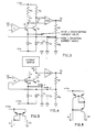
- FIG. 3 there is shown a wideband amplifier circuit in which the effect of stray capacitance Cy present at node y, the inverting (current) input, is cancelled.
- Amplifier A1 in combination with transistors Qx and Qy form an input buffer which causes the voltage at both the inverting current input terminals (nodes x and y) to be equal to the non-inverting input voltage vni.
- resistance Rx would be equal to resistance Ry and Ix would be equal to Iy.
- capacitances Cx and Cy represent a complex impedance composed of the distributed effects of capacitance, resistance, and inductance.
- the best way to duplicate this impedance is to duplicate the physical arrangement of node y at node x. This is done by bringing both nodes out of the amplifier package and duplicating the circuit board trace directly up to the point where resistors Rg and Rf attach at node y. Other conventional means of duplicating this impedance may also be used.
- FIG 4 there is shown an alternative embodiment of the wideband amplifier of Figure 3 that functions to provide the same results.
- Resistors Rx and Ry and voltage gain block A(s) of Figure 3 are replaced by a current mirror and inverting amplifier A(s).
- the current mirror and inverting amplifier A(s) of Figure 4 form an amplifier sensitive to the difference between currents ix and iy.
- the troublesome zero caused by stray capacitance Cy can be cancelled when capacitance Cx is equal to Cy(ix/im) with the current mirror again (im/ix) set for im equal to iy.
- Ix Iy(ix/im).
- Figures 7-9 each illustrate a feedback amplifier circuit with means for eliminating the zero in the transfer function when the input buffer composed of six transistors (Qw, Qwa, Qx, Qxa, Qy, and Qya) replaces the input buffer comprising amplifier A1 and transistors Qx and Qy employed in the circuit of Figures 3 and 4.
- the ratio of the emitter areas of Qx to Qy, Qxa to Qya, and Qwa to Qw should normally be set to 1 to maintain equal DC bias currents for equal base-emitter voltages, although other ratios could be used. When this ratio is set to 1, the equations and analysis presented above in connection with the amplifier circuit of Figure 3 also apply to Figure 7, and the analysis of Figure 4 applies to Figures 8 and 9.
- the transfer function of the inverting amplifier formed by transistor Qs, capacitance cc, current source Is (or current mirror 2 of Figure 9), and amplifier xn can be said to have a transfer function -A(s), to facilitate analysis as described above in connection with the circuit of Figure 4.
- Examples of two possible current mirror circuit configurations are shown in Figures 5 and 6.
- current mirror 1 could be formed by replacing the PNP transistors and positive supply voltage +Vcc of Figures 5 and 6 with NPN transistors and negative supply voltage -Vcc.
- MOS transistors of the correct polarity could also be employed.
- the noninverting amplifier xn would normally be a unity gain amplifier, but amplifiers having other than unity gain could be used.
- current mirror 2 would normally provide gain such that current ratio ic/ib is greater than or equal to 1. This is desirable in order that the slew rate at the collector node of transistor Qs will be greater than the slew rate capability of node y.
- a characteristic of the amplifier circuits of Figures 8 and 9 is that the base current of transistor Qs is not cancelled, and the resulting inverting input bias current will cause an offset voltage at the output vo.
- the circuit of Figure 10 can be used as a replacement for current mirror 1 and transistor Qs in Figure 8 or 9 to reduce the inverting input bias current.
- Transistors Qma and Qmb form a simple current mirror, and the base current ibsb of cascade transistor Qsb is subtracted from current ix, so the collector current of transistor Qmb is given by ix - ibsb.
- iy ix - ibsb + ibsa, where ibsa is the base current of transistor Qsa.
- ibsb ibsa
- iy ix and the net input bias current at node y is zero.
- the emitter currents, the current gain of the two transistors, and the collector-base voltage of the two transistors will not be identical so the inverting input bias current will be much smaller than before, but it will be non-zero.
- the circuit illustrated in Figure 7 also exhibits low input bias current.
- the circuit of Figure 11 also offers input bias current reduction.
- Transistors Qs and Qsm form a current mirror which supplies current to the differential transistor pair Qta and Qtb.
- Other methods of supplying a current bias means for the differential pair of transistors Qta and Qtb would also work as well.
- the PNP current mirror should have a gain of 1 in order to insure that the stable operating point of the differential transistor pair is reached when the collector current of each transistor is equal.
- beta of each transistor will not be strongly affected by Early voltage.
- the compensation terminal designated node x can also be used to receive a current input signal.
- the output voltage vo arising from a current i into node x is identical in magnitude and phase to the voltage vo arising from a current i flowing out of node y.
- the action of negative feedback will seek to cause the current iy to equal the current ix, scaled by the relevant factors Rx/Ry or the gain of current mirror 1, so ix is the independent variable.
- a voltage source connected to node x through a resistor can also be used to supply the current input signal referred to above, but because node x lies outside of the negative feedback path of resistance Rf in general or of the negative feedback path of amplifier A1 in the circuits of Figures 3 and 4, the resulting current ix will be distorted by the nonlinear voltage-to-current conversion properties of transistor Qx.
- a resistor Rg has always been shown to be connected between node y and a ground reference voltage.
- the amplifier operates in a noninverting gain configuration.
- the grounded end of resistor Rg could be connected instead to a second voltage source (vin) for operation in the inverting gain mode.
Landscapes
- Engineering & Computer Science (AREA)
- Power Engineering (AREA)
- Amplifiers (AREA)
Applications Claiming Priority (2)
| Application Number | Priority Date | Filing Date | Title |
|---|---|---|---|
| US06/916,621 US4713628A (en) | 1986-10-08 | 1986-10-08 | Compensation and biasing of wideband amplifiers |
| US916621 | 1986-10-08 |
Publications (2)
| Publication Number | Publication Date |
|---|---|
| EP0263601A2 true EP0263601A2 (de) | 1988-04-13 |
| EP0263601A3 EP0263601A3 (de) | 1989-01-18 |
Family
ID=25437580
Family Applications (1)
| Application Number | Title | Priority Date | Filing Date |
|---|---|---|---|
| EP87308028A Withdrawn EP0263601A3 (de) | 1986-10-08 | 1987-09-11 | Ausgleich und Polarisation von Breitbandverstärkern |
Country Status (3)
| Country | Link |
|---|---|
| US (1) | US4713628A (de) |
| EP (1) | EP0263601A3 (de) |
| JP (1) | JPS63102407A (de) |
Cited By (2)
| Publication number | Priority date | Publication date | Assignee | Title |
|---|---|---|---|---|
| EP0300494A3 (en) * | 1987-07-24 | 1989-08-30 | Nippon Telegraph And Telephone Corporation | Wideband amplifier |
| EP0445879A1 (de) * | 1990-03-07 | 1991-09-11 | Koninklijke Philips Electronics N.V. | Breitband-Signalverstärker |
Families Citing this family (17)
| Publication number | Priority date | Publication date | Assignee | Title |
|---|---|---|---|---|
| US5227737A (en) * | 1990-12-05 | 1993-07-13 | Vtc Inc. | Method and apparatus for adjusting the pole positions of a differentiating amplifier |
| US5196809A (en) * | 1991-03-01 | 1993-03-23 | Fogal William J | High gain, low distortion, faster switching transistor |
| US5420542A (en) * | 1994-05-16 | 1995-05-30 | Elantec, Inc. | Varactor compensation in amplifier circuits |
| US5418495A (en) * | 1994-05-18 | 1995-05-23 | Elantec | Input stage improvement for current feedback amplifiers |
| US5578967A (en) * | 1995-09-28 | 1996-11-26 | Elantec | Circuit compensating for capacitance at inverting input of current feedback amplifier |
| US5760728A (en) * | 1997-02-03 | 1998-06-02 | Motorola, Inc. | Input stage for an analog-to-digital converter and method of operation thereof |
| US6002299A (en) * | 1997-06-10 | 1999-12-14 | Cirrus Logic, Inc. | High-order multipath operational amplifier with dynamic offset reduction, controlled saturation current limiting, and current feedback for enhanced conditional stability |
| CN1143427C (zh) * | 1999-09-02 | 2004-03-24 | 深圳赛意法微电子有限公司 | 互阻放大器 |
| US6429720B1 (en) * | 2000-05-12 | 2002-08-06 | Analog Devices, Inc. | RMS-DC converter using a variable gain amplifier to drive a squaring cell |
| US6466091B1 (en) | 2000-10-02 | 2002-10-15 | Cirrus Logic, Inc. | High order multi-path operational amplifier with reduced input referred offset |
| US6307430B1 (en) | 2000-10-02 | 2001-10-23 | Cirrus Logic, Inc. | Noise reduction technique in chopper stabilized amplifier |
| US6448853B1 (en) * | 2001-04-09 | 2002-09-10 | Elantec Semiconductor, Inc. | Distortion improvement in amplifiers |
| US6885247B2 (en) * | 2001-12-07 | 2005-04-26 | Stmicroelectronics, Inc. | Current amplifier |
| US6515540B1 (en) | 2001-12-10 | 2003-02-04 | Cirrus Logic, Inc. | High order multi-path operational amplifier with output saturation recovery |
| JP2007043540A (ja) * | 2005-08-04 | 2007-02-15 | Alps Electric Co Ltd | バイアス電圧設定機構を備えた増幅回路 |
| US7932783B2 (en) * | 2008-07-25 | 2011-04-26 | Park Larry A | Resonant operating mode for a transistor |
| US8067985B2 (en) * | 2008-08-29 | 2011-11-29 | Park Larry A | Resonant operating mode for a transistor |
Family Cites Families (2)
| Publication number | Priority date | Publication date | Assignee | Title |
|---|---|---|---|---|
| US4358739A (en) * | 1980-02-11 | 1982-11-09 | Nelson David A | Wide-band direct-current coupled transistor amplifier |
| US4502020A (en) * | 1983-10-26 | 1985-02-26 | Comlinear Corporation | Settling time reduction in wide-band direct-coupled transistor amplifiers |
-
1986
- 1986-10-08 US US06/916,621 patent/US4713628A/en not_active Expired - Lifetime
-
1987
- 1987-09-11 EP EP87308028A patent/EP0263601A3/de not_active Withdrawn
- 1987-10-07 JP JP62251736A patent/JPS63102407A/ja active Pending
Cited By (4)
| Publication number | Priority date | Publication date | Assignee | Title |
|---|---|---|---|---|
| EP0300494A3 (en) * | 1987-07-24 | 1989-08-30 | Nippon Telegraph And Telephone Corporation | Wideband amplifier |
| US4885548A (en) * | 1987-07-24 | 1989-12-05 | Nippon Telegraph And Telephone Corporation | Wideband amplifier |
| EP0445879A1 (de) * | 1990-03-07 | 1991-09-11 | Koninklijke Philips Electronics N.V. | Breitband-Signalverstärker |
| US5138278A (en) * | 1990-03-07 | 1992-08-11 | U.S. Philips Corporation | Broadband signal amplifier |
Also Published As
| Publication number | Publication date |
|---|---|
| JPS63102407A (ja) | 1988-05-07 |
| US4713628A (en) | 1987-12-15 |
| EP0263601A3 (de) | 1989-01-18 |
Similar Documents
| Publication | Publication Date | Title |
|---|---|---|
| US4713628A (en) | Compensation and biasing of wideband amplifiers | |
| US5589798A (en) | Input stage improvement for current feedback amplifiers | |
| US5142242A (en) | Precision transconductance amplifier | |
| EP1444777B1 (de) | Ein leistungsverstärkermodul mit verzerrungskompensation | |
| Van de Plassche | A wide-band monolithic instrumentation amplifier [application of voltage-current convertor] | |
| US5351012A (en) | Low input resistance current-mode feedback operational amplifier input stage | |
| US5157322A (en) | PNP transistor base drive compensation circuit | |
| US5315264A (en) | Rail-to-rail opamp with large sourcing current and small quiescent current | |
| US6822514B1 (en) | Amplifier with miller-effect compensation for use in closed loop system such as low dropout voltage regulator | |
| US4881043A (en) | Variable gain transconductance amplifier and variable bandwidth filter | |
| US4956615A (en) | Input circuit for high-frequency amplifiers | |
| US5578967A (en) | Circuit compensating for capacitance at inverting input of current feedback amplifier | |
| US5939944A (en) | NPN push-pull output stage with folded cascode JFETs | |
| EP0314218B1 (de) | Verstärkerschaltung und mit der Verstärkerschaltung versehene Wiedergabeanordnung | |
| US4801893A (en) | Forward transimpedance amplifier | |
| US4425551A (en) | Differential amplifier stage having bias compensating means | |
| US5172017A (en) | Integrated circuit arrangement including a differential amplifier which generates a constant output voltage over a large temperature range | |
| US4779057A (en) | Cascode amplifier with nonlinearity correction and improve transient response | |
| WO1991007816A1 (en) | Difference amplifier employing input attenuator network and powered by a single polarity power supply | |
| JP3022587B2 (ja) | 平衡フィルタ回路 | |
| US5729176A (en) | Linear differential gain stage | |
| US4855684A (en) | Bias current compensation for bipolar input stages | |
| US5237526A (en) | High speed electronic analog computers using low-gain amplifiers | |
| WO1993019523A1 (en) | Distortion cancellation amplifier system | |
| US3631356A (en) | Controllable amplifier stage |
Legal Events
| Date | Code | Title | Description |
|---|---|---|---|
| PUAI | Public reference made under article 153(3) epc to a published international application that has entered the european phase |
Free format text: ORIGINAL CODE: 0009012 |
|
| AK | Designated contracting states |
Kind code of ref document: A2 Designated state(s): DE FR GB |
|
| PUAL | Search report despatched |
Free format text: ORIGINAL CODE: 0009013 |
|
| AK | Designated contracting states |
Kind code of ref document: A3 Designated state(s): DE FR GB |
|
| STAA | Information on the status of an ep patent application or granted ep patent |
Free format text: STATUS: THE APPLICATION IS DEEMED TO BE WITHDRAWN |
|
| 18D | Application deemed to be withdrawn |
Effective date: 19890719 |
|
| RIN1 | Information on inventor provided before grant (corrected) |
Inventor name: NELSON, DAVID A. |