EP0263663A2 - Appareil de traitement d'information dans lequelle des moyens d'effacement sont actionnés pendant une période plus longue que la période nécessaire - Google Patents
Appareil de traitement d'information dans lequelle des moyens d'effacement sont actionnés pendant une période plus longue que la période nécessaire Download PDFInfo
- Publication number
- EP0263663A2 EP0263663A2 EP87308806A EP87308806A EP0263663A2 EP 0263663 A2 EP0263663 A2 EP 0263663A2 EP 87308806 A EP87308806 A EP 87308806A EP 87308806 A EP87308806 A EP 87308806A EP 0263663 A2 EP0263663 A2 EP 0263663A2
- Authority
- EP
- European Patent Office
- Prior art keywords
- erasing
- recording
- information
- recording medium
- information processing
- Prior art date
- Legal status (The legal status is an assumption and is not a legal conclusion. Google has not performed a legal analysis and makes no representation as to the accuracy of the status listed.)
- Granted
Links
Images



Classifications
-
- G—PHYSICS
- G11—INFORMATION STORAGE
- G11B—INFORMATION STORAGE BASED ON RELATIVE MOVEMENT BETWEEN RECORD CARRIER AND TRANSDUCER
- G11B19/00—Driving, starting, stopping record carriers not specifically of filamentary or web form, or of supports therefor; Control thereof; Control of operating function ; Driving both disc and head
- G11B19/02—Control of operating function, e.g. switching from recording to reproducing
- G11B19/04—Arrangements for preventing, inhibiting, or warning against double recording on the same blank or against other recording or reproducing malfunctions
-
- G—PHYSICS
- G11—INFORMATION STORAGE
- G11B—INFORMATION STORAGE BASED ON RELATIVE MOVEMENT BETWEEN RECORD CARRIER AND TRANSDUCER
- G11B11/00—Recording on or reproducing from the same record carrier wherein for these two operations the methods are covered by different main groups of groups G11B3/00 - G11B7/00 or by different subgroups of group G11B9/00; Record carriers therefor
- G11B11/10—Recording on or reproducing from the same record carrier wherein for these two operations the methods are covered by different main groups of groups G11B3/00 - G11B7/00 or by different subgroups of group G11B9/00; Record carriers therefor using recording by magnetic means or other means for magnetisation or demagnetisation of a record carrier, e.g. light induced spin magnetisation; Demagnetisation by thermal or stress means in the presence or not of an orienting magnetic field
- G11B11/105—Recording on or reproducing from the same record carrier wherein for these two operations the methods are covered by different main groups of groups G11B3/00 - G11B7/00 or by different subgroups of group G11B9/00; Record carriers therefor using recording by magnetic means or other means for magnetisation or demagnetisation of a record carrier, e.g. light induced spin magnetisation; Demagnetisation by thermal or stress means in the presence or not of an orienting magnetic field using a beam of light or a magnetic field for recording by change of magnetisation and a beam of light for reproducing, i.e. magneto-optical, e.g. light-induced thermomagnetic recording, spin magnetisation recording, Kerr or Faraday effect reproducing
- G11B11/10502—Recording on or reproducing from the same record carrier wherein for these two operations the methods are covered by different main groups of groups G11B3/00 - G11B7/00 or by different subgroups of group G11B9/00; Record carriers therefor using recording by magnetic means or other means for magnetisation or demagnetisation of a record carrier, e.g. light induced spin magnetisation; Demagnetisation by thermal or stress means in the presence or not of an orienting magnetic field using a beam of light or a magnetic field for recording by change of magnetisation and a beam of light for reproducing, i.e. magneto-optical, e.g. light-induced thermomagnetic recording, spin magnetisation recording, Kerr or Faraday effect reproducing characterised by the transducing operation to be executed
- G11B11/10517—Overwriting or erasing
-
- G—PHYSICS
- G11—INFORMATION STORAGE
- G11B—INFORMATION STORAGE BASED ON RELATIVE MOVEMENT BETWEEN RECORD CARRIER AND TRANSDUCER
- G11B11/00—Recording on or reproducing from the same record carrier wherein for these two operations the methods are covered by different main groups of groups G11B3/00 - G11B7/00 or by different subgroups of group G11B9/00; Record carriers therefor
- G11B11/10—Recording on or reproducing from the same record carrier wherein for these two operations the methods are covered by different main groups of groups G11B3/00 - G11B7/00 or by different subgroups of group G11B9/00; Record carriers therefor using recording by magnetic means or other means for magnetisation or demagnetisation of a record carrier, e.g. light induced spin magnetisation; Demagnetisation by thermal or stress means in the presence or not of an orienting magnetic field
- G11B11/105—Recording on or reproducing from the same record carrier wherein for these two operations the methods are covered by different main groups of groups G11B3/00 - G11B7/00 or by different subgroups of group G11B9/00; Record carriers therefor using recording by magnetic means or other means for magnetisation or demagnetisation of a record carrier, e.g. light induced spin magnetisation; Demagnetisation by thermal or stress means in the presence or not of an orienting magnetic field using a beam of light or a magnetic field for recording by change of magnetisation and a beam of light for reproducing, i.e. magneto-optical, e.g. light-induced thermomagnetic recording, spin magnetisation recording, Kerr or Faraday effect reproducing
- G11B11/10595—Control of operating function
-
- G—PHYSICS
- G11—INFORMATION STORAGE
- G11B—INFORMATION STORAGE BASED ON RELATIVE MOVEMENT BETWEEN RECORD CARRIER AND TRANSDUCER
- G11B7/00—Recording or reproducing by optical means, e.g. recording using a thermal beam of optical radiation by modifying optical properties or the physical structure, reproducing using an optical beam at lower power by sensing optical properties; Record carriers therefor
- G11B7/004—Recording, reproducing or erasing methods; Read, write or erase circuits therefor
- G11B7/0055—Erasing
Definitions
- the present invention relates to an information processing method for erasing information recorded on an erasable recording medium and to an apparatus therefor.
- a magneto-optical recording medium 52 whose cross-section in schematically shown, for example, in Figure lA of the accompanying drawings is known as an erasable recording medium.
- This magneto-optical recording medium has as a recording layer 53 a magnetic film whose readily magnetizable axis is perpendicular to the film surface. Recording of information may be accomplished by arranging the directions of magnetization of the recording layer 53 in one direction in advance, and scanning the recording layer by a light beam 54 intensity-modulated in conformity with the information while extraneously applying a magnetic field M R in the direction opposite to said one direction.
- the portion of the recording layer to which the light beam is applied is once demagnetized, and then is magnetized in the opposite direction to the other portion by an extraneous magnetic field and forms a recording bit 55 corresponding to the information as shown in Figure lB of the accompanying drawings.
- the thus recorded information may be read out in a well-known manner using the magneto-optical effect by applying an unmodulated light beam of low intensity to the recording layer and detecting the light reflected by or transmitted through the recording layer.
- a light beam 56 is applied to the area in which the information is recorded while an extraneous magnetic field M E in the opposite direction to the direction during recording (i.e., the direction in which the recording layer was magnetized before recording) is applied to the recording layer as shown in Figure 1C of the accompanying drawings.
- a magneto-optical recording medium is generally divided into predetermined units called sectors. Each sector in turn is divided into an address area and a recording area, and a gap portion is provided therebetween.
- an address area an address number or the like indicative of the position of that sector on the medium is pre-recorded by an unerasable bit 58 formed by the unevenness or the like of the medium substrate.
- the recording bit 57 is magnetically recorded by the afore-described method. Also, this sector is separated from the next sector by a sector gap.
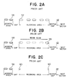
- the recording area may be scanned by an erasing light beam spot 59 as shown in Figure 2B.
- unerased portions 60 of the recording bit are caused as shown in Figure 2C of the accompanying drawings. Such unerased portions 60 have caused a reduction in the reliability of recording when information is re-recorded in this area.
- the above object of the present invention is achieved by driving, in an information processing method for scanning by erasing means a recording medium on which information is recorded in a predetermined area and erasing the recorded information, the erasing means for a period including the period during which the erasing means is on said area and longer than the period.
- an information processing apparatus comprises recording erasing means for applying light beam to an optical recording medium and selectively effecting recording and erasing of information, scanning means for scanning the light beam relative to the recording medium, and control means for controlling the application time of the light beam so that during erasing, the light beam is applied to an area larger than the area of the recording medium in which information is recorded.
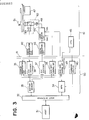
- FIG. 3 is a block diagram showing an embodiment of the present invention applied to a magneto-optical information recording apparatus.
- reference numeral 31 designates a host computer
- reference numeral 61 denotes a disk drive
- reference numeral 50 designates a controller for controlling the operation of the drive 61
- reference numeral 32 denotes a host interface connecting the host computer 31 and the controller 50 together
- reference numeral 41 designates a drive interface connecting the drive 61 and the controller 50 together.
- a magnetooptical disk 46 is mounted in the drive 61 and may be rotated by a spindle motor 47.
- a light beam is applied to the rotated disk 46 from an optical head 62, whereby recording, reproduction and erasing of information are effected.
- the optical head 62 includes a semiconductor laser 48 which is a light source, an optical system for condensing the light beam emitted from the semiconductor laser onto the disk, and a photodetector 49 for detecting the reflected light from the disk.
- the drive 61 has a digital demodulating circuit 42, a digital modulating circuit 43, a laser driving circuit 44, a drive side central processing unit (CPU) 45 and an extraneous magnetic field applying means 51.
- the controller 50 contains therein a buffer memory 33, a micro processing unit (MPU) 34, an address regenerating circuit 35, an error correction code (ECC) decoder 36, an ECC encoder 37, a write gate control circuit 38, a read gate control circuit 39 and a command status 40.
- MPU micro processing unit
- ECC error correction code
- an instruction to effect recording of information is supplied from the CPU 45 to the MPU 34 through the command status 40.
- a read gate signal S RG is supplied from the read gate control circuit 39 to the laser driving circuit 44.
- the semiconductor laser 48 continuously emits a light at the read mode, i.e., at a low intensity, and the light beam is scanned on the disk 46.
- the reflected light from the disk 46 is detected by the photodetector 49, and the detection signal is input to the address regenerating circuit 35 through the digital demodulating circuit 42.
- the address number recorded on the disk 46 is regenerated by the address regenerating circuit 35.
- an enable signal is output from the address regenerating circuit 35 to the write gate control circuit 38.
- a write gate signal S WG corresponding to the recording area on the disk 46 is output from the write gate control circuit 38 to the laser driving circuit 44.
- the recorded information is once stored from the host computer 31 into the buffer memory 33 through the host interface 32.
- a recording signal is input to the laser driving circuit 44 through the ECC encoder 37 and the digital demodulating circuit 43.
- an operation similar to that described above is performed until an enable signal is output from the address regenerating circuit 35.
- an instruction of the erasing mode is provided from the MPU 34 to the write gate control circuit 38 and a gate signal longer than during recoridng is output.
- the laser driving circuit causes the semiconductor laser to emit a light for the period of time during which said gate signal is in its ON state. Thereby, the light beam is scanned over an area longitudinally longer than the recording area, i.e., an area from a gap to a sector gap. Accordingly, even if more or less error occurs in the scannong direction, erasing of information can be reliably accomplished.
- FIG. 4 A specific example of the construction of the write gate control circuit 38 is shown in Figure 4.
- reference numerals 1 and 2 designate gate signal ON control circuits
- reference numerals 3 and 4 denote gate signal OFF control circuits.
- These control circuit each are comprised of a counter and a plurality of transister logics (TTL), and are designed to output a pulse corresponding to one clock and stop when the count of the counter reaches a predetermined value.
- Reference numerals 5 and 6 designate latches, and reference numerals 8, 9, 10 and 11 denote the output lines from the respective control circuits.
- Reference numeral 12 designates a gate signal
- reference numeral 13 denotes a circuit selecting control signal input from the MPU 34
- reference numeral 14 designates a counter operating enable signal input from the address regenerating circuit
- reference numeral 15 denotes a clock signal input from an internal clock signal generator, not shown
- reference numeral 18 designates a multiplexer.
- control circuits 1 and 2 are for data recording and the control circuits 3 and 4 are for data erasing.
- the multiplexer 18 selects a terminal A in response to the control signal 13 from the MPU 34 so that the gate signal 12 is controlled by the control circuits 1 and 2.
- the enable signal 14 input from the address regenerating circuit 35 becomes active as shown in Figure 5A
- the counters in the control circuits 1 and 2 start to count the clock signal 15 as shown in Figures 5B and 5D.
- the set value of the counter in the control circuit 1 is made smaller than the set value of the counter in the control circuit 2.
- a coincidence pulse as shown in Figure 5C is output to the line 8 and latched by the latch 5, and the output 16 shown in Figure 5F becomes active.
- the set value of the counter in the control circuit 2 is greater than the set value of the counter in the control circuit 1 and therefore, after the coincidence pulse of Figure 5C has been output, the count value of the counter in the control circuit 2 becomes equal to the set value and the coincidence pulse shown in Figure 5E is output to the line 10.
- the output 16 is reset by the latch 5 as shown in Figure 5F. Since the multiplexer 18 selects the terminal A, the output 16 is intactly input as a gate signal 12 to the aforementioned laser driving circuit 44.
- the gate signal 12 assumes the gate timing during recording shown in Figure 6.
- the multiplexer 18 selects a terminal B in response to the control siganl 13 from the MPU 34 and change-over is made so that the gate signal 12 is controlled by the control circuits 3 and 4.
- the enable signal 14 input from the address regenerating circuit 35 becomes active, the counters in the control circuits 3 and 4 start to count the clock signal 15 as during recording.
- the set value of the counter in the control circuit 3 is made smaller than the set value of the counter in the control circuit 4.
- a coincidence pulse is output to the line 9 and is latched by the latch 6, and the output 17 becomes active.
- the set value of the counter in the control circuit 4 is greater than the set value of the counter in the control circuit 3 and therefore, after a coincidence pulse has been output to the line 9, the count value of the counter in the control circuit 4 becomes equal to the set value and a coincidence pulse is output to the line 11.
- the output 17 is reset by the latch 6. Since the multiplexer 18 selects the terminal B, the output 17 is input as a gate signal 12 to the aforementioned laser driving circuit 44.
- the gate timing during erasing shown in Figure 6 is obtained.
- the driving of the semiconductor laser 44 in Figure 3 is effected in accordance with these gate timings.
- FIG 7 is a block diagram showing another example of the construction of the write gate control circuit in the apparatus shown in Figure 3.
- discrete circuits are provided to vary the allowed laser turn-on period by the gate signal between the recording time and the erasing time, whereas in the present example, control of the gate signal is effected by one kind of control circuit.
- reference numeral 20 designates a gate signal ON control circuit
- reference numeral 21 denotes a gate signal reset control circuit
- reference numerals 22 and 23 designate latches for setting the counters in the control circuits
- reference numeral 24 denotes a gate signal outputting latch
- reference numeral 25 designates a gate signal
- reference numerals 26 and 27 denote the output lines from the respective control circuits
- reference numeral 28 designates the MPU bus from the MPU
- reference numeral 29 denotes the enable signal from the address regenerating circuit
- reference numeral 30 designates the clock signal from an internal clock signal generator, not shown.
- such a set value is latched by the latch 22 that the coincidence pulse of the control circuit 20 is output from the MPU bus 28 to the line 26 by the MPU 34 upon termination of the gap of Figure 6. Also, such a set value is latched by the latch 23 that the coincidence pulse of the control circuit 21 is output upon termination of the recording area.
Landscapes
- Optical Recording Or Reproduction (AREA)
Applications Claiming Priority (2)
| Application Number | Priority Date | Filing Date | Title |
|---|---|---|---|
| JP23801886A JPS6394410A (ja) | 1986-10-08 | 1986-10-08 | 情報処理装置 |
| JP238018/86 | 1986-10-08 |
Publications (3)
| Publication Number | Publication Date |
|---|---|
| EP0263663A2 true EP0263663A2 (fr) | 1988-04-13 |
| EP0263663A3 EP0263663A3 (en) | 1989-07-12 |
| EP0263663B1 EP0263663B1 (fr) | 1992-09-16 |
Family
ID=17023933
Family Applications (1)
| Application Number | Title | Priority Date | Filing Date |
|---|---|---|---|
| EP19870308806 Expired EP0263663B1 (fr) | 1986-10-08 | 1987-10-05 | Appareil de traitement d'information dans lequelle des moyens d'effacement sont actionnés pendant une période plus longue que la période nécessaire |
Country Status (3)
| Country | Link |
|---|---|
| EP (1) | EP0263663B1 (fr) |
| JP (1) | JPS6394410A (fr) |
| DE (1) | DE3781759T2 (fr) |
Families Citing this family (1)
| Publication number | Priority date | Publication date | Assignee | Title |
|---|---|---|---|---|
| JP2823152B2 (ja) * | 1996-08-30 | 1998-11-11 | 株式会社日立製作所 | 情報の記録再生方法 |
Family Cites Families (3)
| Publication number | Priority date | Publication date | Assignee | Title |
|---|---|---|---|---|
| JPS6063772A (ja) * | 1983-09-19 | 1985-04-12 | Olympus Optical Co Ltd | デ−タ書込エリア信号発生方法および装置 |
| JPS60258733A (ja) * | 1984-06-05 | 1985-12-20 | Matsushita Electric Ind Co Ltd | 消去可能な光学的記録再生装置 |
| KR910001328B1 (ko) * | 1985-10-08 | 1991-03-04 | 마쯔시다덴기산교 가부시기가이샤 | 정보기록재생장치 |
-
1986
- 1986-10-08 JP JP23801886A patent/JPS6394410A/ja active Pending
-
1987
- 1987-10-05 DE DE19873781759 patent/DE3781759T2/de not_active Expired - Fee Related
- 1987-10-05 EP EP19870308806 patent/EP0263663B1/fr not_active Expired
Also Published As
| Publication number | Publication date |
|---|---|
| JPS6394410A (ja) | 1988-04-25 |
| EP0263663A3 (en) | 1989-07-12 |
| DE3781759D1 (de) | 1992-10-22 |
| EP0263663B1 (fr) | 1992-09-16 |
| DE3781759T2 (de) | 1993-03-18 |
Similar Documents
| Publication | Publication Date | Title |
|---|---|---|
| KR860000636A (ko) | 광자기 정보 기록장치 | |
| EP0429343B1 (fr) | Appareil d'enregistrement utilisant l'effet magnéto-optique | |
| EP0376818A2 (fr) | Appareil pour l'enregistrement magnéto-optique sur disque | |
| US5293361A (en) | Information processing method and apparatus therefor in which an erasing device is driven for a period longer than a necessary period | |
| US4901169A (en) | Data recording apparatus able to accurately access a floppy disk regardless of recording density | |
| EP0263663A2 (fr) | Appareil de traitement d'information dans lequelle des moyens d'effacement sont actionnés pendant une période plus longue que la période nécessaire | |
| US4916557A (en) | Method of sharing various types of medium drives and recording/reproduction apparatus with medium controller for realizing the method | |
| US5452273A (en) | Optical recording method and apparatus therefor | |
| EP0267586A2 (fr) | Appareil pour commander des équipements périphériques | |
| US4875202A (en) | Disk-type storage medium recording/reproducing apparatus | |
| JP2584795B2 (ja) | 光磁気情報記録及び消去装置 | |
| EP0346063A2 (fr) | Méthode d'enregistrement magnéto-optique et appareil pour celle-ci | |
| JP2597627B2 (ja) | 磁気記録再生装置及び同装置に適用するデータ記録制御装置 | |
| JP2794839B2 (ja) | 記録再生装置 | |
| JPH0612562B2 (ja) | 磁気記録再生装置 | |
| JPH052828A (ja) | 磁気デイスク記録再生装置 | |
| JPH06243528A (ja) | 光情報記録再生装置 | |
| JPS6297136A (ja) | 消去可能な光学的記録再生装置 | |
| JP2517898B2 (ja) | 光学記録方法及びその装置 | |
| JP2748444B2 (ja) | 光磁気記録装置 | |
| JP2853364B2 (ja) | 光磁気ディスク装置 | |
| JPS62266751A (ja) | 光学式情報記録再生装置 | |
| JPS62208444A (ja) | 光磁気記録方法 | |
| JPH02249107A (ja) | ポジショニング制御方式 | |
| JPH06111407A (ja) | 光磁気ディスク装置 |
Legal Events
| Date | Code | Title | Description |
|---|---|---|---|
| PUAI | Public reference made under article 153(3) epc to a published international application that has entered the european phase |
Free format text: ORIGINAL CODE: 0009012 |
|
| AK | Designated contracting states |
Kind code of ref document: A2 Designated state(s): DE FR GB IT NL |
|
| PUAL | Search report despatched |
Free format text: ORIGINAL CODE: 0009013 |
|
| RHK1 | Main classification (correction) |
Ipc: G11B 19/04 |
|
| AK | Designated contracting states |
Kind code of ref document: A3 Designated state(s): DE FR GB IT NL |
|
| 17P | Request for examination filed |
Effective date: 19891201 |
|
| 17Q | First examination report despatched |
Effective date: 19901220 |
|
| GRAA | (expected) grant |
Free format text: ORIGINAL CODE: 0009210 |
|
| AK | Designated contracting states |
Kind code of ref document: B1 Designated state(s): DE FR GB IT NL |
|
| REF | Corresponds to: |
Ref document number: 3781759 Country of ref document: DE Date of ref document: 19921022 |
|
| ET | Fr: translation filed | ||
| ITF | It: translation for a ep patent filed | ||
| RIN2 | Information on inventor provided after grant (corrected) |
Free format text: AIZAWA, TAKAYUKI NO. 1115, YOKOMIZO DAINI MANSHON |
|
| PLBE | No opposition filed within time limit |
Free format text: ORIGINAL CODE: 0009261 |
|
| STAA | Information on the status of an ep patent application or granted ep patent |
Free format text: STATUS: NO OPPOSITION FILED WITHIN TIME LIMIT |
|
| 26N | No opposition filed | ||
| ITTA | It: last paid annual fee | ||
| REG | Reference to a national code |
Ref country code: GB Ref legal event code: IF02 |
|
| PGFP | Annual fee paid to national office [announced via postgrant information from national office to epo] |
Ref country code: GB Payment date: 20050921 Year of fee payment: 19 |
|
| PGFP | Annual fee paid to national office [announced via postgrant information from national office to epo] |
Ref country code: NL Payment date: 20051018 Year of fee payment: 19 |
|
| PGFP | Annual fee paid to national office [announced via postgrant information from national office to epo] |
Ref country code: FR Payment date: 20051027 Year of fee payment: 19 |
|
| PGFP | Annual fee paid to national office [announced via postgrant information from national office to epo] |
Ref country code: DE Payment date: 20051216 Year of fee payment: 19 |
|
| PGFP | Annual fee paid to national office [announced via postgrant information from national office to epo] |
Ref country code: IT Payment date: 20061031 Year of fee payment: 20 |
|
| PG25 | Lapsed in a contracting state [announced via postgrant information from national office to epo] |
Ref country code: NL Free format text: LAPSE BECAUSE OF NON-PAYMENT OF DUE FEES Effective date: 20070501 Ref country code: DE Free format text: LAPSE BECAUSE OF NON-PAYMENT OF DUE FEES Effective date: 20070501 |
|
| GBPC | Gb: european patent ceased through non-payment of renewal fee |
Effective date: 20061005 |
|
| NLV4 | Nl: lapsed or anulled due to non-payment of the annual fee |
Effective date: 20070501 |
|
| REG | Reference to a national code |
Ref country code: FR Ref legal event code: ST Effective date: 20070629 |
|
| PG25 | Lapsed in a contracting state [announced via postgrant information from national office to epo] |
Ref country code: GB Free format text: LAPSE BECAUSE OF NON-PAYMENT OF DUE FEES Effective date: 20061005 |
|
| PG25 | Lapsed in a contracting state [announced via postgrant information from national office to epo] |
Ref country code: FR Free format text: LAPSE BECAUSE OF NON-PAYMENT OF DUE FEES Effective date: 20061031 |