EP0263745B1 - Verfahren und Vorrichtung zum Messen der Frequenz eines elektrischen Signals - Google Patents
Verfahren und Vorrichtung zum Messen der Frequenz eines elektrischen Signals Download PDFInfo
- Publication number
- EP0263745B1 EP0263745B1 EP19870402175 EP87402175A EP0263745B1 EP 0263745 B1 EP0263745 B1 EP 0263745B1 EP 19870402175 EP19870402175 EP 19870402175 EP 87402175 A EP87402175 A EP 87402175A EP 0263745 B1 EP0263745 B1 EP 0263745B1
- Authority
- EP
- European Patent Office
- Prior art keywords
- signal
- counter
- measurement period
- given direction
- measurement
- Prior art date
- Legal status (The legal status is an assumption and is not a legal conclusion. Google has not performed a legal analysis and makes no representation as to the accuracy of the status listed.)
- Expired - Lifetime
Links
Images


Classifications
-
- G—PHYSICS
- G01—MEASURING; TESTING
- G01R—MEASURING ELECTRIC VARIABLES; MEASURING MAGNETIC VARIABLES
- G01R23/00—Arrangements for measuring frequencies; Arrangements for analysing frequency spectra
- G01R23/02—Arrangements for measuring frequency, e.g. pulse repetition rate; Arrangements for measuring period of current or voltage
Definitions
- the present invention relates to a method and a device for measuring the frequency of an electrical signal.
- a first object of the present invention is to make it possible to measure the frequency of a signal capable of evolving in a wide range of frequencies, for example of the order of 2 Hz to 20KHz.
- Another object of the present invention is to provide a method and a device for measuring frequency operating in a wide range with an accuracy at least equal to one percent, in a time not exceeding 0.5 s.
- Another object of the present invention is to provide a method and a device for measuring a frequency which is not stable over time.
- Measuring a frequency can be done in two ways: either as a frequency meter or as a period meter
- Frequency meter operation consists of measuring the frequency of a signal by counting the number of pulses or switching of the same direction of the signal during a determined unit time.
- this measurement technique is not satisfactory when it is a question of measuring a relatively low frequency with good precision, because this technique requires a very long measurement time. For example, to measure a frequency of the order of 2 Hz with an accuracy of 1%, according to the frequency meter technique, it is necessary to count 100 periods signal, which requires a measurement time of 50 seconds.
- Periodimeter operation consists in measuring the signal period by counting the number of clock pulses contained in a signal period.
- This measurement technique is however not satisfactory when it comes to measuring, with good precision, a relatively high frequency, because this measurement technique then requires a very fast frequency clock.
- a frequency of the order of 20 KHz or more precisely a period of 50 ⁇ s with an accuracy of 1% it is necessary to have a clock of 2 MHz.
- the microprocessor defines a measurement time of predetermined fixed duration.
- the synchronism door detects the first cycle of the input signal which occurs immediately after the start of the measurement time and triggers the opening of the main door and the secondary door during this detection.
- the synchronism door also detects the first cycle of the input signal which occurs immediately after the end of the measurement time and triggers the closing of the main door and the secondary door, during this detection.
- the opening and closing of the main door and the secondary door are defined by a signal called "door control”.
- This "door control” signal is therefore synchronized with the input signal. Its duration is not fixed and predetermined but corresponds to a multiple of the period of the input signal.
- the frequency measurement is obtained by dividing the number of pulses contained in the event counter by the number of pulses contained in the time counter.
- the frequency meter described in the above-mentioned document only works correctly for a measurement time greater than the period of the signal to be measured. Indeed, the frequency meter described in this document does not work if the start of a cycle of the input signal does not occur during the measurement time.
- the period of the clock signal is approximately 100 times shorter than the duration of time.
- the duration of the measurement time is between 40 and 200 ms, preferably being of the order of 50 msec.
- the frequency of the signal is obtained by multiplying by the frequency of the clock signal, the result of the ratio between on the one hand, the number of edges of the signal calculated in step iii) and d on the other hand, the number of clock pulses calculated in step v).
- the present invention also relates to a device for measuring the frequency of an electrical signal for implementing the above method.
- the device according to the invention is distinguished by the fact that the detection means which detect the signal edges are connected to the assembly which defines the time of measurement of predetermined fixed duration and act on this set to synchronize the origin of the measurement time Tf on a first edge of given direction of the signal.
- the device illustrated schematically in Figure 3 is suitable for measuring the respective frequency of three electrical signals applied respectively to the main inputs 10, 11 and 12 of the device.
- the device illustrated in FIG. 3 comprises three calculation modules 100A, 100B, 100C, two multiplexing modules 200A, 200B, a division module 300, three output modules 400A, 400B and 400C and a management module 500.
- the calculation modules 100A, 100B and 100C are suitable for calculating quantities N and K, which will be explained below, representative respectively of the frequency of the signals applied to the inputs 10, 11 and 12.
- the 200A module ensures the sequential multiplexing of the aforementioned N parameters from the modules 100A, 100B and 100C.
- the module 200B ensures the multiplexing of the parameters K originating from the modules 100A, 100B and 100C.
- the division module 300 calculates the ratio between the above parameters N and K.
- the purpose of the output modules 400A, 400B and 400C is to store the result of the calculation coming from the divider module 300, corresponding respectively to the signals applied to the inputs 10, 11 and 12.
- management module 500 is to synchronize the general operation of the aforementioned modules 100, 200, 300 and 400.
- the first line of this figure schematically illustrates a logic signal S whose frequency is to be measured.
- the second line of FIG. 1 schematically illustrates a signal T whose steps define measurement windows Tf of determined duration.
- the third line in FIG. 1 illustrates a clock signal He of constant frequency Fe.
- the measurement method according to the present invention consists in counting the number N of edges of a given direction, for example, the number of rising edges, the signal S during the measurement window Tf, counting from number K of clock pulses generated between the detection of the first edge of given direction (for example the first rising edge) of the signal S during the measurement window Tf, and the appearance of the first edge of the same direction consecutive to the expiry of the measurement window Tf, then making the relationship between on the one hand, the number N of edges of the signal S calculated during the measurement window Tf and on the other hand, the number K of clock pulses.
- the number K of clock pulses calculated between the detection of the first edge of the given direction of the signal during the measurement window Tf and the appearance of the first edge of the same consecutive direction is illustrated diagrammatically in the fourth line of FIG. 1 at the end of the measurement window Tf.
- the error made on the measurement is at most equal to one clock pulse out of K clock pulses counted.
- the measurement error is maximum when the signal period corresponds substantially to the duration of the measurement window Tf.
- N 1 and the error measurement is equal to 1 / K, K being equal to the number of clock pulses counted during the window Tf.
- the period of the clock signal He must be 100 times less than the duration of the measurement window Tf.
- FIG. 1a a schematic illustration of the measurement error on the frequency is shown in percent as a function of the frequency of the input signal.
- FIG. 1bis corresponds to the aforementioned case where the period of the clock signal He is 100 times shorter than the duration of the measurement window Tf.
- the error is maximum and equal to 1% when the signal period is equal to the duration of the measurement window Tf.
- the number N increases progressively, in regular steps, corresponding to the multiples 1 / Tf as illustrated in Figure 1bis, and for each of the growth steps of the number N, the number K of clock pulses counted, decreases between N.100 / (N - 1) and 100.
- the measurement error is defined by a series of discontinuous increasing stairs, the slope of which decreases and which level off at 1% as illustrated in the figure. 1 bis.
- FIG. 2 illustrates the shape of the response of the measuring device according to the present invention to a sudden change in frequency input. More specifically, FIG. 2 illustrates the response of the device for different values of the duration of the measurement window Tf.
- the representation of FIG. 2 results from a simulation carried out by calculation. This simulation shows that the dynamic error is the smallest when the window Tf is the smallest possible. However, this simulation has shown that if we take a window smaller than 50ms the response is no longer monotonous, we see oscillations appear. These oscillations are not admissible insofar as they would have repercussions on the output display unit.
- the Applicant has determined that the optimum measurement time Tf is located around 50 ms.
- the Applicant has also determined that the period of the optimum clock signal was around 500 ⁇ s.
- the Applicant has chosen a measurement window duration Tf equal to 48.8 ms and a period of the clock signal equal to 488 ⁇ s, value determined by 1 / 211.
- modules 100A, 100B and 100C are identical.
- these modules 100 receive as input the signal S whose frequency it is desired to measure, a basic timing signal H, a general reset signal R.
- the circuit 100 outputs a multibit signal Vn representing the number N of signal periods counted during the measurement window Tf, a multi-bit signal VK representing the value of the number K of clock pulses counted between the appearance of the first rising edge of the signal during the measurement window and the first rising edge of the signal consecutive to the expiration of the measurement window, a signal Z indicating that the frequency of the signal to be measured is less than a predetermined frequency and that under these conditions the result of the measurement is zero, and finally a signal DD addressed to the management module 500 and indicating the appearance of a new measurement result, in order to initiate the calculation of the corresponding N / K ratio.
- the circuit 100 illustrated in FIG. 4 comprises a sub-assembly 110 which aims to determine the duration of the measurement window Tf, a sub-assembly of time which delivers the clock signal He, two counters 160, 170 which have the purpose of determining the numbers N and K respectively, a sub-assembly 175 which detects a frequency lower than the minimum frequency to be measured, and exit gates 180, 190 associated respectively with the counters 160 and 170 for memorizing the numbers N and K.
- the sub-assembly 110 which aims to determine the duration of the measurement window Tf receives as input the timing signal H, the general reset signal R and an auxiliary reset signal generated by the synthesis module 130 as will be decreased later.
- the timing signal H is preferably 1 MHz. This timing signal H is applied to the input of an inverter 122 whose output attacks the clock input CKA of a counter 123.
- the QA output of this counter 123 is looped back to the clock input CKB of the counter 123.
- the latter receives on its reset input CLR the general reset signal R.
- the inputs of an AND gate with two inputs 112 are connected respectively to the output QD of the counter 123 and to the output of the subset 110 composed by the output of an OR gate 121.
- the output of the AND gate 112 attacks the clock input CLK of a counter 113.
- the reset input RST of this counter 113 is connected at the output of an OR gate 111.
- the inputs of the latter are connected respectively to the general reset input R and to the reset output of the synthesis sub-assembly 130, formed by the output of an AND 140 door.
- the outputs Q1 to Q13 of the counter 113 are connected to the inputs of an OR gate 121 via 5 inverters 114, 115, 116, 117, 118, an OR gate 119 with three inputs and a NOR port 120.
- the outputs Q1, Q5, Q9, Q10 and Q13 of the counter 113 are connected respectively to the inputs of the inverters 114, 115, 116, 117 and 118.
- the inputs of the OR gate 119 are connected respectively to the outputs of the inverters 114 and 115 and to the output Q4 of the counter 113.
- the inputs of the NOR gate 13 are connected respectively to the outputs Q6, Q7, Q8, Q11 and Q12 of the counter 113 and to the outputs of the inverters 116, 117 and 118.
- the inputs of the OR gate 121 are respectively connected to the output of the OR gate 119 and NOR gate 120.
- the OR gate 121 In the event that the timing signal H has a frequency of 1 MHz, the OR gate 121 generates at the output tops of 2 ⁇ s of duration with a period of 48.8 ms.
- the duration of the tops of 2 ⁇ s is defined by the counter 123.
- the period of 48.8 ms of the tops originating from the OR gate 121 is determined by counting the counter 113.
- the period of tops from OR gate 121 corresponds to the duration of the measurement window Rf sought.
- the purpose of the synthesis module 130 is to generate at the output two signals intended respectively to control the storage of the values N and K in the output buffers 180, 190 on the one hand, and to reinitialize the counters 160, 170 and reset the sub-assembly 110 on the other hand.
- the sub-assembly 130 receives as input the timing signal H, the general reset signal R, the signal S whose frequency it is desired to measure, and the signal Tf generated at the output of the above-mentioned OR gate 121.
- the timing signal H is applied to the input of an inverter 131.
- the general reset signal R is applied to the input of an inverter 132 whose output drives inputs PR of two flip-flops 136, 138 of the JK type mounted in cascade.
- the signal S is applied to the input of an inverter 133.
- the signal Tf from the OR gate 121 is applied to the input of an inverter 134.
- the inputs of an AND gate 135 with two inputs are connected respectively to the outputs of the two inverters 133 and 134 above.
- the output of the gate ET 135 attacks the input K of the flip-flop 136.
- the clock input CK of this flip-flop 136 is connected to the output of the inverter 131.
- the input J of the flip-flop 136 is connected to the output Q of the flip-flop 138.
- the reset input CLR of the flip-flop 136 is connected to a positive supply voltage + Vcc.
- the Q output of flip-flop 136 attacks a first input of an AND gate 140.
- the second input of this AND gate 140 is linked to the Q output of flip-flop 138.
- the exit Q of flip-flop 136 is connected to a first input of an AND gate 137 whose second input receives signal S whose frequency is to be measured.
- the output of the AND gate 137 is connected to the input J of the flip-flop 138.
- Clock entry CK of the flip-flop 138 is connected to the output of the inverter 131.
- the input K of the flip-flop 138 receives the signal Tf coming from the OR gate 121.
- the reset input CLR of flip-flop 138 is connected to a positive supply voltage + Vcc.
- the output Q of the flip-flop 138 attacks, in addition to the input J of the flip-flop 136, a first input of the AND gate 139, the second input of which is connected to the output Q of scale 136.
- the output of the AND gate 139 generates a pulse coinciding with the detection of the first rising edge of the consecutive signal at the measurement window Tf to control the storage of the values N and K defined by the counters 160 and 170 in the output buffers 180 and 190.
- the output of gate 140 generates a pulse coinciding with the start of the measurement window Tf to reset the counters 160 and 170 and to reset the sub-assembly 110.
- the purpose of the sub-assembly 150 is to divide the frequency of the timing signal H to obtain the above-mentioned clock signal He.
- the timing signal H is applied to the input of an inverter 151 whose output attacks the clock input CLK of a counter 154.
- the reset input RST of the counter 154 is connected to the output of an OR gate 153. This receives, on the one hand, the reset signal general R and the signal from the output Q a D 158 rocker.
- the clock input CK of the flip-flop 158 is connected via an inverter 152 to the output of the inverter 151.
- the entrees PR and CLR of flip-flop 158 are connected to a positive supply voltage + Vcc.
- the input D of the flip-flop 158 is connected via a NAND gate 157 and two inverters 155 and 156 to the outputs Q1 to Q9 of the flip-flop 154.
- the outputs Q4 and Q5 of the counter 154 are connected to the inputs of the inverters 155 and 156 respectively.
- the inputs of the NAND157 gate are connected to the inputs Q1 to Q3 and Q6 to Q9 of the counter 154 and to the outputs of the inverters 155 and 156.
- the counter 154 is arranged to count 488 pulses of the timing signal H and therefore the output Q of flip-flop 158 generates pulses with a duration of 1 ⁇ s with a period of 488 ⁇ s. This signal corresponds to the clock signal He sought.
- the counter 160 counts the number of periods of the signal S contained in the measurement window Tf.
- the counter 160 receives on its clock input CLK the signal S and on its reset input RST the signal from an OR gate 176 controlled by the module 130 and more precisely by the exit from the above-mentioned door ET 140.
- the number N available at the output of the counter 160 is stored in two buffers 182, 184 formed for example each of ten flip-flops D mounted in parallel.
- the outputs of flip-flops 182 and 184 are connected to an output bus 186, for example a 10-bit bus.
- the storage of the number N determined by the counter 160 in the flip-flops 182, 184 is controlled by the signal from the AND gate 139 applied to the clock inputs CK of flip-flops 182 and 184.
- the counter 170 counts the number of clock pulses He contained between the first rising edge of the signal during the measurement window Tf and the first rising edge of the signal consecutive to the expiration of the measurement window Tf.
- the counter 170 receives on its clock input CLK the clock signal He from the output Q of flip-flop 158.
- the reset input RST of the counter 170 is connected to the output of the above-mentioned OR gate 176.
- the outputs of the counter 170 are connected to the inputs of flip-flops D grouped together for example in the form of two circuits 192 and 194 the outputs of which are connected to a second multibit output bus 196, for example at 10 bits.
- the number K of clock pulses He counted by the counter 170 is available on the bus 196.
- the storage of the number K in the flip-flops D 192 and 194 is controlled by the clock signal from the AND gate 139 applied to the clock inputs CK of circuits 192 and 194.
- the module 175 intended to detect that the frequency to be measured is less than a predetermined frequency is composed of the above-mentioned OR gate 176 and a flip-flop D 177.
- the input D of the latter is connected to the output Q 11 of the counter 170.
- the change to "1" of the output Q11 of the counter 170 means that the counter 170 has exceeded a predetermined value corresponding to a measurement frequency less than 2Hz.
- the clock input CK of the flip-flop 177 is connected to the output of the inverter 131.
- the input PR of flip-flop 177 and connected to the output of an inverter 101 which receives as input the general reset signal R.
- the output Q of flip-flop 177 is connected to an input of OR gate 176. This receives on its other inputs the general reset signal R and the output of the AND gate 140.
- the signal Z indicating that the measurement result is zero because the frequency is less than a minimum measurement frequency is available on the output Q of the flip-flop 177.
- the signal DD indicating that the result of a new measurement is available in view of a division is generated on the output of gate ET 139.
- the numbers N generated by each of the circuits 100A, 100B and 100C and available on the output buses 186A, 186B and 186C, are multiplexed by signals A, B, C coming from the management circuit 500.
- the numbers K generated by each of the subsets 100A, 100B and 100C and available on the output buses 196A, 196B and 196C are multiplexed by the subassembly 200B using the same signals A, B and C generated by the management module 500.
- the multiplexing subsets 200A and 200B are identical.
- This circuit includes 30 AND doors with two inputs and 10 OR doors with three inputs.
- the AND gates are grouped in groups of three, such as the group consisting of AND gates 202, 204 and 206.
- the different groups of three AND gates are associated respectively with bits of different weight of the signals applied to the output buses 186 or 196 of the calculation circuits 100.
- One of the inputs of the three gates of each group is respectively connected to a line associated bit of buses 186A, 186B, 186C, or 196A, 196B and 196C.
- the other input of the three doors of this group respectively receives the multiplexing signals A, B and C generated by the management module 500.
- the outputs of the doors of the same group are connected to the respective inputs of an associated OR door.
- the output of this OR gate is connected to a line of an output bus 201.
- the numbers N generated by the calculation modules 100A, 100B and 100C are multiplexed by the module 200A and available on the 10-bit bus 201A applied to the division module 300.
- the numbers K generated by the calculation modules 100A, 100B and 100C are multiplexed by the module 200B and available on the 10-bit bus 210B applied to the management module 300.
- This circuit receives as input the signals DD from the AND gates 139 of the calculation modules 100A, 100B and 100C (referenced respectively DD1, DD2, and DD3 in FIG. 6), the timing signal H, the general reset signal R, a signal DB generated by the divider module 300 to indicate whether it is available for further division.
- the management circuit 500 generates at the output the multiplexing signals A, B and C applied to the multiplexing modules 200A, 200B, a signal CD for division control applied to the divider circuit 300, and signals BR1, BR2 and BR3 applied respectively to the output buffer stages 400A, 400B and 400C.
- the timing signal H and the general reset signal R are applied to the inputs of reversers 514 and 516 respectively.
- the signals DD1, DD2 and DD3 from the AND gates 139 integrated into the calculation modules 100A, 100B and 100C respectively are applied to the clock input CK of flip-flops D 502, 504 and 506.
- the latter have their inputs D and PR connected to a positive supply voltage + Vcc.
- CLR flip-flops 502, 504 and 506 are connected respectively at the ET 508, 510 and 512 door exits.
- One of the inputs of these AND gates 508, 510 and 512 is connected to the output of the inverter 516.
- AND gates 508, 510 and 512 receives a signal respectively BR1 , BR2 and BR3 whose generation will be explained later.
- the Q and Q of flip-flop 502 which generate signals referenced respectively D1 and D1 are connected to respective lines of an auxiliary bus 501.
- the signal DB is also applied to one of the associated lines of the auxiliary bus 501, as is the output of the inverter 518 receiving the above-mentioned signal DB as an input.
- auxiliary bus 503. This receives the signals H and R from inverters 514 and 516 as well as signals J1, J2, J3, K2 and K3 generated at the output of OR gates 540, 554, 556, 558 and 560 in a manner which will be described in more detail below.
- Reset inputs CLR JK 520, 522 and 524 scales receive the signal R .
- Clock inputs CK flip-flops 520, 522 and 524 receive the timing signal H .
- the J input of flip-flop 520 receives the J1 signal.
- the input K of the flip-flop 520 is connected to the positive supply voltage + Vcc.
- the inputs J and K of the flip-flop 522 receive the signals J2 and K2 respectively.
- the inputs J and K of the flip-flop 524 receive the signals J3 and K3 respectively.
- the Q and Q flip-flops 520, 522 and 524 are connected to a third auxiliary bus 505.
- the outputs Q and Q of flip-flop 520 generate signals Q1 and Q1 respectively.
- the Q and Q of flip-flop 522 generate signals Q2 and Q2 respectively.
- the outputs Q and Q of flip-flop 524 generate signals Q3 and Q3 respectively.
- the inputs of an AND gate 526 receive signals Q2 and DB .
- the inputs of an ET 528 gate with 3 inputs respectively receive the signals Q2 , Q3 and DB .
- the outputs of AND gates 526 and 528 are connected to the inputs of an OR gate 540 which outputs the above-mentioned signal J1 applied to the auxiliary bus 503.
- the inputs of a NOR 530 gate with 4 inputs respectively receive the signals Q3, D1, D2 and D3.
- the inputs of an AND gate with two inputs 542 are respectively connected to the signal line Q2 and at the exit of door NOR 530.
- the inputs of an AND 544 gate with two inputs respectively receive the signals D1 and D3.
- the inputs of a NOR 532 gate with 4 inputs respectively receive the signals Q1, Q2, Q3 and DB.
- OR gate 544 The inputs of an OR gate 544 with 3 inputs are connected respectively to the output of AND gates 542 and 544 and to the output of NOR gate 532.
- OR gate 554 which generates the above-mentioned signal J2 is connected to the bus auxiliary 503.
- the inputs of an AND gate with 3 inputs 534 respectively receive the signals Q2, Q3 and DB .
- the inputs of an AND gate with two inputs 546 receive the signals Q1 and Q3 respectively.
- the output of the OR gate 556 which generates the above-mentioned signal K2 is connected to the auxiliary bus 503.
- the inputs of a NOR gate with 4 inputs 536 respectively receive the signals Q1, Q2 , Q3 and DB.
- the inputs of an AND gate with three inputs 548 respectively receive the signals Q1 , DB and D2.
- the inputs of an AND gate with two inputs 552 respectively receive the signals DB and D1.
- OR gate 558 with 3 inputs are connected respectively to the output of NOR gate 536 and to the outputs of AND gates 548 and 552.
- the output of the OR gate 558 which generates the aforementioned signal J3 is connected to the auxiliary bus 503.
- the inputs of an ET 538 gate with two inputs receive the signals Q2 and DB .
- the inputs of an AND gate with two inputs 550 receive the signals Q1 and Q2.
- OR 560 gate with two inputs are connected respectively to the outputs of AND gates 538 and 550.
- the output of the OR gate 560 which generates the aforementioned signal K3 is connected to the auxiliary bus 503.
- An OR gate with two inputs 562 receives signals Q2 and Q3.
- the inputs of an AND gate with two inputs 576 respectively receive the signal from the OR gate 562 and the signal Q1 .
- the division control signal CD applied to the divider 300 is available at the output of the AND gate 576.
- An AND gate 564 with three inputs receives signals Q1, Q2 and Q3 .
- the output of gate 564 generates the signal BR1 applied to the output buffer 400A. Furthermore, the output of the AND gate 564 is connected to the input of an inverter 578. The latter generates the signal as an output. BR1 applied to the entry of the above-mentioned door ET 508.
- the inputs of an AND gate 566 with three inputs receive signals Q1, Q2 and Q3 respectively.
- the AND gate 566 generates at output the signal BR2 applied to the output buffer 400B.
- gate ET 566 is also connected to the input of a 580 inverter. The latter outputs the signal BR2 applied to the aforementioned ET 510 door.
- the inputs of an AND gate 568 with three inputs respectively receive the signals Q1, Q2 and Q3.
- the output of the AND gate 568 delivers the signal BR3 applied to the output buffer 400C.
- the output of the AND gate 568 is also connected to the input of an inverter 582 which generates the signal as an output.
- BR3 applied to the aforementioned ET 512 gate.
- the inputs of an AND gate with three inputs 570 respectively receive the signals Q1 , Q2 and Q3.
- the output of the AND gate 570 generates as output the multiplexing signal A applied to the modules 200A and 200B.
- the inputs of an AND gate 572 with three inputs respectively receive the signals Q1 , Q2 and Q3.
- the output of the AND gate 572 generates the signal B applied to the multiplexing modules 200A and 200B.
- the inputs of an AND gate 574 with three inputs respectively receive the signals Q1 , Q2 and Q3 .
- the output of the AND gate 574 generates the multiplexing signal C applied to the modules 200A and 200B.
- the divider circuit 300 is adapted to calculate the ratio between the numbers N and K delivered respectively by each of the modules 100A, 100B and 100C, and provide the result in floating point for example with 8 bits of mantissa and 4 bits of exhibitor.
- the fact of using a divider circuit 300 which delivers the floating point result makes it possible to greatly limit the number of output bits.
- the mantissa and exponent values of the result delivered by the divider circuit 300 are stored in the output buffers 400A, 400B and 400C associated respectively with the signals applied to the inputs 10, 11 and 12.
- the output buffers 400A, 400B and 400C are of identical structure.
- FIG. 7 The structure of such an output buffer is illustrated diagrammatically in FIG. 7.
- this output buffer comprises flip-flops D mounted in parallel and grouped for example in the form of two circuits 402, 404.
- the divider circuit 300 generates its floating point output signal with 8 bits of mantissa and 4 bits of exponent
- 6 flip-flops D receive via a bus 302 the bits of mantissa from the divider circuit 300, while 4 flip-flops D receive from a bus 304 the exponent bits from the divider circuit 300.
- the Q outputs of the flip-flops are available on a 12-bit output bus 406.
- the storage of mantissa and exponent data from the divider circuit 300 is validated by the pulses BR i generated by the management circuit 500 and applied to the clock inputs CK of the flip-flops 402, 404.
- the resetting of the output buffers 402 and 404 is ensured either when the frequency of the signal is lower than a predetermined frequency, by example 2Hz according to the embodiment described above, ie during the general reset.
- an OR gate 410 receives the above-mentioned signals Z and R respectively.
- the output of the OR gate 410 generates a signal CL which indicates to the downstream circuit capable of using the result representative of the frequency available on the output bus 406 that new sequential information has just been stored in the buffers of exit 402 and 404.
- calculation modules 100A, 100B and 100C determine in parallel the numbers N and K representative of the frequency of the signals S1, S2 and S3 applied respectively to the inputs 10, 11 and 12.
- the numbers N and K associated with the signal S1, coming from the module 100A, are available on the buses 186A and 196A.
- the numbers N and K associated with the signal S2 from the module 100B are available on the output buses 186B and 196B.
- Buses 186A, 186B, 186C are applied to the inputs of the multiplexing module 200 A. Similarly, the buses 196A, 196B and 196C are connected to the inputs of the muliplexing device 200B.
- the multiplexing module 200A sequentially samples the signals representative of the numbers N coming from the calculation modules 100A, 100B and 100C. Simultaneously, the 200B multiplexing module samples in sequence the signals representative of the numbers K from the calculation modules 100A, 100B and 110C.
- the outputs of the multiplexing modules 200A and 200B are applied to the dividing member 300.
- the latter therefore successively calculates the mantissa and the exponent of the quotient N / K associated respectively with the signals S1, S2 and S3.
- the values of the mantissa and the quotient exponent, coming from the divider 300 are stored respectively in the output buffers 400A, 400B and 400C.
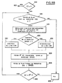
- FIG. 8 schematically illustrates an operating flow diagram of the divider circuit 300.
- the divider circuit comprises a register called DQ which initially stores the dividend, a register called AC initialized to zero and a register called DR which initially receives the divider.
- the register AC being initialized to zero, the dividend being placed in the register DQ and the divider in the register DR, a first shift of the rank of the contents of the registers AC and DQ is carried out to the left, then we subtract the divider from the contents of the AC register. If the carry is equal to 1, the least weight of the DQ register is defined as being equal to zero and the next operation to be performed corresponds to an addition of the previous content of the AC register and of the content of the DR register, the result of this addition being used to refresh the AC register.
- the carry is equal to zero, it is determined that the least weight of the DQ register is equal to 1 and the next operation to be performed corresponds to a subtraction consisting in subtracting the content of the DR register from the previous content of the AC register and to refresh the content of the register AC with the result of the subtraction.
- the mantissa of the quotient is then in the register DQ while the exponent is available at the output of a counter which was triggered at the initialization of the second phase and incremented at each cycle thereof.
- the first step 600 of the process consists in initializing to zero a flip-flop called BRES which aims to restore bit 2 n of the register AC, to store the dividence N in the register DQ, to store the divider K in the DR register, to initialize the AC register to zero, to carry out the resetting of a counter CE capable of restoring the value of the exhibitor and to resetting a CI counter which records the number of operations in the division process.
- BRES flip-flop
- the second step 602 of the division method consists in shifting the content of the registers AC and DQ by one row to the left and in incrementing the iteration counter CI by one unit.
- the division process then consists in detecting whether or not the content of the flip-flop BRES is equal to 1, if yes the bit 2 n of the register AC being equal to 1, we proceed to step 606 adding the contents of the AC register and the contents of the DR register and refreshing the contents of the AC register with the result of the addition.
- step 608 a subtraction, by removing the content of the register DR of the content of the AC register and a refresh of the content of the AC register by the result of the subtraction.
- Step 612 is followed by the interrogation step 614 of verifying whether the number of increments of the counter CI, that is to say the number of iterations of the division process is equal to the number n of bits numbers N and K. Otherwise, the above process is reiterated from step 602. If yes, the first phase of the division process is finished, the quotient is available at the DQ register and the rest in the AC register.
- step 614 is followed by the second phase of the disision process aimed at delivering the floating point quotient in the form of a mantissa and an exponent.
- step 616 it is sought whether the highest weight of the DQ register is equal to 1. If yes, the division process is terminated in step 632. If no, that is to say if the highest weight of the DQ register is equal to 0, step 616 is followed by step 618 consisting in effecting a new shift to the left of a row of the contents of the registers AC and DQ and incrementing the counter CE exhibitor of a unit.
- step 620 It is then sought in step 620 if the content of the BRES flip-flop is equal to 1.
- step 622 If yes, that is to say if the bit 2 n of the register AC is equal to 1, we proceed to step 622 to the addition of the content of the registers AC and DR and to the updating of the content of the flip-flop AC with the result of the addition.
- step 624 If not, that is to say if the bit 2 n of the register AC is equal to zero, one proceeds to a subtraction by withdrawal of the content of the register DR from the content of the register AC and to the refreshment of the content of the register AC by the result of the subtraction, as shown in step 624.
- Steps 622 and 624 are followed by step 626 consisting in transferring the weight 2 n of the register AC into the flip-flop BRES.
- Step 626 is followed by step 628 consisting in making the lowest weight of the register DQ equal to the complement of the content of the flip-flop BRES.
- Step 628 is followed by the interrogation step 630 consisting in determining whether the number of increments of the second phase, that is to say the content of the counter CE is equal to 2 n-1 .
- step 614 if not, that is to say if the number of iterations of the second consecutive phase in step 614 has not reached 2 n-1 , the second phase of the division process is repeated from from step 616.
- step 632 When the division process is finished in step 632, the mantissa of the quotient N / K is available in the register DQ, while the exponent is available at the output of the counter CE which was triggered at the revival of the second phase of the division process (consecutive to step 614) and incremented with each cycle, when passing through step 618.
- the binary adders 312, 313 and 314, formed for example of type 74HC283 housing are connected by their input A to respective outputs of the aforementioned OR gates 301 to 311.
- the latter receive on one of their inputs the output Q of the flip-flop BRES 330.
- the second inputs of the OR gates 301 to 311 respectively receive one of the bits of the signal representing the number K coming from the calculation circuit 100, via the multiplexer 200A.
- the outputs E of the adders 312, 313 and 314 are connected to the inputs of the registers AC 315, 316 and 317. The output of these registers is applied to the inputs B of the adders 312, 313 and 314.
- the output Q of the flip-flop BRES 330 is at zero, the output of doors 301 to 311 represents the divider DR.
- the output Q of the flip-flop BRES 330 being also connected to the low weight retainer C0 of the first adder 312, the output of the adders 312, 313 and 314 represents the result of the addition AC + DR, that is to say the addition of the content of the registers AC and of the signal DR present at the output of the OR gates 301 to 311.
- the exit Q of the flip-flop BRES 330 is at 1
- the output of the doors OR 301 to 311 represents the complement to 2 of the divider DR, that is DR .
- the restraint C0 of the adder 312 is also at 1.
- a signal representing the result of the operation AC + is then obtained at the output of the adders 312, 313 and 314 DR +1, or a signal corresponding to the AC - DR subtraction.
- the output of the OR gate 321 attacks the input of the register 323.
- OR gate 321 The inputs of OR gate 321 are connected respectively to the output of AND gates 319 and 320.
- a first input of the AND gate 319 receives a multiplexing signal MUX generated by the management circuit 350, by means of an inverter 318.
- the second input of the AND gate 319 receives the least significant bit of the dividend, namely N dis in figure 9.
- the first input of the ET 320 port is connected to the output Q of the BRES scale.
- the second input of the AND gate 320 receives the above-mentioned multiplexing signal MUX.
- the registers 324, 325 and 326 receive as input the signal bits representing the dividing N and generate at the output, for example on an eight bit bus 302, the mantissa signal N.
- the general reset signal R is applied to the input of an inverter 327.
- the latter attacks the first input of an AND gate 329.
- the second input of the AND gate 329 is connected to the output d an inverter 328 which itself receives as input a CLR signal generated by the management circuit 350 in a manner which will be described in more detail below.
- the output of the inverter 328 is also connected to the zero reset inputs of registers 315, 316 and 317.
- gate ET 329 attacks the reset input CLR of the BRES 330 scale.
- the counter CE which determines the value of the exponent comprises in cascade a counter 333 five bits and an adder 334 four bits.
- the reset input RST of counter 333 receives the aforementioned CLR signal.
- the clock input CLK of the counter 333 is connected to the output of an AND gate 332.
- the inputs thereof receive signals V4 and CC respectively generated by the management circuit 350 in a manner which will be described in more detail below.
- the inputs Q1 to Q5 of the counter 333 attack the inputs A2, B1, B2, B3 and B4 of the 4-bit adder 334.
- the inputs A1, A3 and A4 of the latter are connected to a positive supply voltage + Vcc.
- the retaining entry C0 of the adder 334 is connected to ground.
- the output Q1 of the counter 333 determines the least significant weight of the exponent, the three most significant bits being determined by the outputs E1, E2 and E3 of the adder 334.
- the 4 exponent bits thus formed are available on the 4-bit output bus 304 which corresponds to the output Q1 of the counter 333 and to the outputs E1, E2 and E3 of the adder 334.
- the output Q6 of the counter 333 is also connected to a first input of an OR gate 331.
- the second input of the latter is connected to the output QA of the last box 326 of the dividend register DQ.
- the output of the OR gate 331 which generates a signal referenced MSBMQ is applied to the divider management circuit 350.
- the management circuit 350 receives as input the timing signal H, the general reset signal R, the signal MSBMQ available at the output of the OR gate 331, and the signal CD delivered by the management circuit 500 at the output of the gate ET 576.
- the general reset signal R is applied to the input of an inverter 351.
- the latter receive on their clock input CK the timing signal H.
- the input J of the flip-flop 352 receives a signal 03 generated in a manner which will be described in more detail below.
- the input K of the flip-flop 352 is connected to the output Q of the flip-flop 353.
- the Q and Q of flip-flop 352 generate signals P3 and P3 applied to an auxiliary bus 380.
- the input J of the flip-flop 353 is connected to the output Q of the flip-flop 352.
- the input K of the flip-flop 353 receives a signal 02 generated in a manner which will be described in more detail below.
- the Q and Q of flip-flop 353 generate signals P2 and P2 applied to the auxiliary bus 380.
- the input J of the flip-flop 354 receives a signal 01 generated in a manner which will be described in more detail below.
- the input K of the flip-flop 354 is connected to the output Q of this flip-flop.
- the Q and Q of flip-flop 354 generate signals P1 and P1 applied to the auxiliary bus 380.
- the MSBMQ signal from OR gate 331 is applied to an inverter 356.
- the latter generates an output signal F applied to another auxiliary bus 381.
- the output of the inverter 356 is also connected to the input of an inverter 355 which generates an output signal F applied to the auxiliary bus 381.
- a DC signal generated in a manner which is described in more detail below is applied to the input of an inverter 358.
- the latter generates a signal at the output. E applied to the auxiliary bus 381.
- the output of the inverter 358 which generates an output signal E applied in the same way to the auxiliary bus 381.
- the signal CD generated by the management circuit 500, at the output of the AND gate 576, is applied to the input of an inverter 360.
- the latter generates a signal at the output D applied to the auxiliary bus 381.
- the output of the inverter 360 is also connected to the input of an inverter 359 which generates an output signal D applied in the same way to the auxiliary bus 381.
- An AND gate with two inputs 361 receives the signals P2 and P3 and generates as output the aforementioned signal 01 applied to an auxiliary bus 382.
- a NAND gate 362 with 4 inputs receives the signals D, E, F and P1 respectively.
- the output of the NAND gate 362 is connected to the input of an inverter 366, the output of which generates the aforementioned signal 02 applied to the auxiliary bus 382.
- An AND gate with three inputs 362 receives the signals D, P1 and P2 .
- An AND gate 364 with three inputs receives signals P1, E and F .
- An AND gate with two inputs 365 receives the signals P1 and E .
- OR gate 367 The inputs of an OR gate 367 with three inputs are connected respectively to the outputs of gates 363, 364 and 365.
- the output of OR gate 367 generates the aforementioned signal 03 applied to the auxiliary bus 381.
- An AND gate with three inputs 368 receives the signals respectively P1 , P3 and the timing signal H.
- the output of the AND gate 368 generates a signal V1 applied to the clock inputs CK of the registers 324, 325 and 326, as well as to the first input of an OR gate 322 whose output is connected to the clock input CK of register 323.
- the inputs of an AND gate with three inputs 369 respectively receive the signals P1 , P2 and the timing signal H.
- the output of gate ET369 generates a signal V2 applied to the clock inputs CK of registers AC 315, 316 and 317.
- the signal V3 applied V3 applied to the clock input CK of the flip-flop BRES 330 corresponds to the signal P1 available on the auxiliary bus 380.
- An AND gate with two inputs 370 receives the signals P1 and the timing signal H.
- the output of the AND gate 370 delivers a signal V4 applied to the second input of the OR gate 322.
- An AND gate with three inputs 371 receives the signals P1 , P2 and P3.
- the AND gate 371 generates an SL signal applied to the SH / inputs LD registers 315, 316, 317, 323, 324, 325 and 326.
- An AND 372 gate with three inputs receives the signals P1 , P2 and P3.
- the output of the AND gate 372 generates the aforementioned CLR signal.
- gate E 372 is also applied to a first input of an OR gate 374 with two inputs, the second input of which receives the general reset signal R.
- the output of the OR gate 374 is connected to the reset input CLR of a counter 376 forming the counter CI.
- Entrance AT of this counter is connected to the output of a NAND 375 door.
- the inputs of the latter are connected respectively to the output of the above-mentioned AND gate 370 and to the output of a NAND gate 377.
- the outputs QB and QD of the counter 376 are respectively connected to the inputs of the NAND gate 377.
- the output of the latter is connected, in addition to one of the inputs of the NAND gate 375 to the input of an inverter 378.
- the latter outputs the DC signal applied to one of the inputs of the AND gate 332.
- An OR gate with two inputs 373 receives signals P2 and P3.
- the output of the OR gate 373 generates the signal DB.
- This signal is 1 when a division is in progress. On the other hand, it is zero when the divider has finished its calculation or when it is waiting for a division request.
- the signal DB can be used by a downstream circuit using the frequency of the signal in the form of the mantissa M and the exponent E.
- the mantissa of the quotient is available on 8 bits at the level of the bus 302 connected to the registers 324, 325 and 326.
- the exponent of the quotient N / K is available in 4 bits on the output bus 304 connected to the counter 333 and to the adder 334.
- the circuit illustrated diagrammatically in FIG. 3 is produced in the form of an integrated circuit.
Landscapes
- Physics & Mathematics (AREA)
- General Physics & Mathematics (AREA)
- Measuring Frequencies, Analyzing Spectra (AREA)
- Measurement Of Unknown Time Intervals (AREA)
Claims (22)
- Verfahren zum Messen der Frequenz eines elektrischen Signals (S) der Art, welches die Verfahrensschritte umfaßt, die darin bestehen:i) eine Meßzeit (Tf) von vorgegebener, fester Dauer zu definieren,ii) die Fronten einer vorgegebenen Richtung, ansteigend oder fallend, des zu messenden Signals (S) festzustellen und Gattersteuerungssignale zu erzeugen, die einerseits mit der ersten Front der vorgegebenen Richtung des Signals (S) während der Meßzeit (Tf) synchronisiert sind und andererseits mit der ersten Front der gegebenen Richtung des folgenden Signals (S) nach dem Verstreichen der Meßzeit (Tf) synchronisiert sind,iii) in einem ersten Zähler die Anzahl (N) der Fronten der gegebenen Richtung des Signals (S) zwischen der ersten Front der gegebenen Richtung des Signals (S) während der Meßzeit (Tf) und der ersten Front der gegebenen Richtung des folgenden Signals (S) nach dem Verstreichen der Meßzeit (Tf) zu zählen,iv) ein Taktsignal (He) konstanter Frequenz zu erzeugen,v) in einem zweiten Zähler die Anzahl (K) der Taktimpulse, die zwischen der ersten Front der gegebenen Richtung des Signale (S) während der Meßzeit (Tf) und der ersten Front der gegebenen Richtung des folgenden Signale (S) nach dem Verstreichen der Meßzeit (Tf) erzeugt werden, zu zählen, undvi) das Verhältnis zwischen auf der einen Seite der von dem ersten Zähler gezählten Anzahl (N) von Fronten des Signals (S) und auf der anderen Seite der von des zweiten Zähler gezählten Anzahl (K) von Taktimpulsen zu bilden,
gekennzeichnet durch die Tatsache, daß die Detektion der Fronten des Signals (S) ausgewertet wird, indem der Ursprung der Meßzeit (Tf) mit einer ersten Front gegebener Richtung des Signale (S) synchronisiert wird. - Meßverfahren nach Anspruch 1, gekennzeichnet durch die Tatsache, daß die Periode des Taktsignals (He) ungefähr 100 mal geringer ist als die Dauer der Meßzeit (Tf).
- Meßverfahren nach einem der Ansprüche 1 oder 2, gekennzeichnet durch die Tatsache, daß die Dauer der Meßzeit (Tf) zwischen 40 und 100 ms liegt, wobei sie vorzugsweise in der Größenordnung von 50 ms liegt.
- Meßverfahren nach einem der Ansprüche 1 bis 3, gekennzeichnet durch die Tatsache, daß die Frequens des Signals (S) erhalten wird, indem man die Frequens des Taktsignals (He) mit dem Ergebnis des Verhältnisses zwischen auf der einen Seite der Anzahl (N) von Signalfronten, die in Schritt (ii) berechnet wurde, und auf der anderen Seite der Anzahl (K) von Taktimpulsen, die in Schritt (v) berechnet wurde, multipliziert.
- Vorrichtung zum Messen der Frequenz eines elektrischen Signale (S) zum Ausführen des Verfahrens nach einem der Ansprüche 1 bis 4, des Typs, der umfaßt:- eine Anordnung (110), die eine Meßzeit (Tf) von vorgegebener, fester Dauer definiert,- Detektorvorrichtungen (130), die die Fronten einer vorgegebenen Richtung, ansteigend oder fallend, des zu messenden Signals (S) feststellen und Gattersteuerungssignale erzeugen, die einerseits mit der ersten Front der vorgegebenen Richtung des Signals (S) während der Meßzeit (Tf) synchronisiert sind und andererseits mit der ersten Front der gegebenen Richtung des folgenden Signals (S) nach dem Verstreichen der Meßzeit (Tf) synchronisiert sind,- einen ersten Zähler (160), der von den Gattersteuerungssignalen gesteuert wird und der die Anzahl (N) der Fronten der gegebenen Richtung des Signals (S) zwischen der ersten Front der gegebenen Richtung des Signals (S) während der Meßzeit (Tf) und der ersten Front der gegebenen Richtung des folgenden Signale (S) nach dem Verstreichen der Meßzeit (Tf) zählt,- einen Taktgeber (150), der ein Taktsignal (He) konstanter Frequenz erzeugt,- einen zweiten Zähler (170), der von den Gattersteuerungssignalen gesteuert wird und die Anzahl (K) der Taktimpulse, die zwischen der ersten Front der gegebenen Richtung des Signals (S) während der Meßzeit (Tf) und dar ersten Front der gegebenen Richtung des folgenden Signals (S) nach dem Verstreichen dar Meßzeit (Tf) erzeugt werden, zählt, und- eine Zelle (300), die geeignet ist, das Verhältnis zwischen auf der einen Seite der von dem ersten Zähler (180) gezählten Anzahl (N) von Fronten des Signals (S) und auf der anderen Seite der von dem zweiten Zähler (170) gezählten Anzahl (K) von Taktimpulsen zu bilden,
gekennzeichnet durch die Tatsache, daß die Detektionsvorrichtungen (130), die die Fronten des Signals (S) feststellen, mit der Anordnung (110) verbunden sind, die die vorgegebene, feste Meßzeit (Tf) definieren, und auf diese Anordnung einwirken, um den Ursprung der Meßzeit (Tf) mit einer ersten Front gegebener Richtung des Signals (S) zu synchronisieren. - Meßvorrichtung nach Anspruch 5, gekennzeichnet durch die Tatsache, daß die Periode des Taktsignals (He) ungefähr 100 mal geringer ist als die Dauer der Meßzeit (Tf).
- Meßvorrichtung nach einem der Ansprüche 5 oder 6, gekennzeichnet durch die Tatsache, daß die Dauer der Meßzeit (Tf) zwischen 40 und 100 ms liegt, wobei sie vorzugsweise in der Größenordnung von 50 ms liegt.
- Meßvorrichtung nach einem der Ansprüche 5 bis 7, gekennzeichnet durch die Tatsache, daß die Periode des Taktsignals (He) in der Größenordnung von 500 µs liegt.
- Meßvorrichtung nach einem der Ansprüche 5 bis 8, die erlaubt, die Frequenz von mehreren elektrischen Signalen zu messen, gekennzeichnet durch die Tatsache, daß sie umfaßt:- mehrere Verarbeitungsmodule (100A, 100B, 100C), die jeweils umfassen:- eine Anordnung (110), die eine Meßzeit (Tf) von vorgegebener, fester Dauer definiert,- Detektorvorrichtungen (130), die die Fronten einer vorgegebenen Richtung, ansteigend oder fallend, eines entsprechenden, damit verbundenen Signals (S) feststellen und Gattersteuerungssignale erzeugen, die einerseits mit der ersten Front der vorgegebenen Richtung des Signals (S) während der Meßzeit (Tf) synchronisiert sind und andererseits mit der ersten Front der gegebenen Richtung des folgenden Signals (S) nach dem Verstreichen der Meßzeit (Tf) synchronisiert sind,- einen ersten Zähler (160), der von den Gattersteuerungssignalen gesteuert wird und der die Anzahl (N) der Fronten der gegebenen Richtung des Signals (S) zwischen der ersten Front der gegebenen Richtung des Signals (S) während der Meßzeit (Tf) und der ersten Front der gegebenen Richtung des folgenden Signals (S) nach dem Verstreichen der Meßzeit (Tf) zählt,- einen Taktgeber (150), der ein Taktsignal (He) konstanter Frequenz erzeugt,- einen zweiten Zähler (170), der von den Gattersteuerungssignalen gesteuert wird und die Anzahl (K) der Taktimpulse, die zwischen der ersten Front der gegebenen Richtung des Signale (S) während der Meßzeit (Tf) und der ersten Front der gegebenen Richtung des folgenden Signale (S) nach dem Verstreichen der Meßzeit (Tf) erzeugt werden, zählt,- zwei Multiplexermodule (200A, 200B), die jeweils eine Anzahl von Eingängen gleich der Anzahl von Verarbeitungsmodulen (100A, 100B, 100C) und einen einzigen Ausgang besitzen, die am Eingang einerseits Signale (VN₁, VN₂, VN₃) empfangen, die den Inhalt jedes der ersten Zähler darstellen, und andererseits Signale (VK₁, VK₂, VK₃) empfangen, die den Inhalt jedes der zweiten Zähler darstellen, um diese Signale zu multiplexen,- eine einzige Berechnungszelle (300), die sequentiell und der Reihe nach, das Verhältnis zwischen der von dem ersten Zähler (160) gezählten Anzahl (N) und der von dem zweiten Zähler (170) gezählten Anzahl (K) jedes der Verarbeitungsmodule (100A, 100B, 100C) bildet, und- Speicherzellen (440A, 440B, 440C) in einer Anzahl gleich der Anzahl der Verarbeitungsmodule (100A, 100B, 100C), die geeignet sind, jeweils das von der einzigen Berechnungszelle bestimmte Ergebnis, das einem damit verbundenen Signal entspricht, zu speichern.
- Meßvorrichtung nach einem der Ansprüche 5 bis 9, gekennzeichnet durch die Tatsache, daß jede Anordnung (110) einen Zähler (113) umfaßt, der an seines Takteingang ein Basistaktsignal (H) erhält und dessen Ausgänge mit logischen Gattern (114-121) verbunden sind, die ein Signal (Tf) erzeugen, das die Meßzeit einer vorgegebenen, festen Dauer angibt.
- Meßvorrichtung nach einem der Ansprüche 5 bis 10, gekennzeichnet durch die Tatsache, daß die Detektion der ersten Front einer vorgegebenen Richtung des Signals (S) nach dem Verstreichen der Meßzeit (Tf) durch eine Anordnung logischer Gatter (133, 134, 135, 137) und von Kippschaltungen (138, 138) durchgeführt wird.
- Meßvorrichtung nach einem der Ansprüche 5 bis 11, gekennzeichnet durch die Tatsache, daß jeder Taktgeber (150) einen Zähler (154) umfaßt, der an seinem Takteingang ein Basistaktsignal (H) erhält und dessen Ausgänge mit logischen Gattern (155, 156, 157) verbunden sind, die am Ausging das Taktsignal (He) erzeugen.
- Meßvorrichtung nach einem der Ansprüche 5 bis 12, gekennzeichnet durch die Tatsache, daß der erste Zähler (160) das Signal, dessen Frequenz man messen möchte, an seinem Takteingang (CLK) empfängt und an seinem Reset-Eingang (RST) einen Rechteckimpuls erhält, dessen Periode dem Zeitintervall entspricht, das den Ursprung der Meßzeit (Tf) von der ersten Front gegebener Richtung den Signals (S), die nach dem Verstreichen der Meßzeit folgt, trennt.
- Meßvorrichtung nach einem der Ansprüche 5 bis 13, gekennzeichnet durch die Tatsache, daß der zweite Zähler (170) das Taktsignal (He) an seinem Takteingang (CLK) empfängt und an seinem Reset-Eingang (RST) einen Rechteckimpuls erhält, dessen Periode dem Zeitintervall entspricht, das den Ursprung der Meßzeit (Tf) von der ersten Front gegebener Richtung des Signals (S), die nach dem Verstreichen dieser Meßzeit folgt, trennt.
- Meßvorrichtung nach einem der Ansprüche 6 bis 14, gekennzeichnet durch die Tatsache, daß einer der höherwertigen Ausgänge des zweiten Zählers (170) ein Signal (Z) erzeugt, das anzeigt, daß die Frequenz des Eingangssignals niedriger ist als eine vorgegebene Meßschwelle.
- Meßvorrichtung nach einem der Ansprüche 5 bis 15, gekennzeichnet durch die Tatsache, daß Speicherpuffer (182, 184, 192, 194) an die Ausgänge der ersten und zweiten Zähler (160, 170) angeschlossen sind.
- Meßvorrichtung nach einem der Ansprüche 5 bis 18 in Verbindung mit Anspruch 9, gekennzeichnet durch die Tatsache, daß jedes Multiplexermodul (200A, 200B) aus einer Anordnung von logischen Qattern (202, 298) gebildet ist.
- Meßvorrichtung nach einem der Ansprüche 5 bis 17 in Verbindung mit Anspruch 9, gekennzeichnet durch die Tatsache, daß die Speicherzellen (404A, 404B, 404C), die geeignet sind, das von der Berechnungszelle bestimmte Ergebnis zu speichern, aus Kippschaltungen (402, 404) gebildet sind.
- Meßvorrichtung nach einem der Ansprüche 5 bis 18, gekennzeichnet durch die Tatsache, daß jede Berechnungszelle (300) das Resultat des Verhältnisses von auf der einen Seite der Anzahl (N) von während des Meßfensters (Tf) von dem ersten Zähler gezählten Fronten und von auf der anderen Seite der Anzahl (K) von von dem zweiten Zähler (170) gezählten Taktimpulsen als Fließkommazahl in der Form einer Mantisse und eines Exponenten erzeugt.
- Meßvorrichtung nach Anspruch 19, gekennzeichnet durch die Tatsache, daß sie wenigstens eine Speicherzelle (400) umfaßt, die eine erste Unteranordnung (402), die geeignet ist, die Mantisse zu speichern, und eine zweite Unteranordnung (404), die geeignet ist, den Exponenten zu speichern, umfaßt.
- Meßvorrichtung nach einem der Ansprüche 5 bis 20, gekennzeichnet durch die Tatsache, daß jede Berechnungszelle (300) umfaßt;- ein Hauptregister (DQ, 324, 325, 326), das anfänglich den Dividenden speichert, der der während der Meßzeit von dem ersten Zähler (160) gezählten Anzahl (N) von Fronten entspricht,- ein Hilfsregister (AC, 315, 316, 317), das auf Null zurückgesetzt ist, und- ein sekundäres Register (DR, 301-311), das anfänglich den Divisor erhält, der der Anzahl (K) von durch den zweiten Zähler (170) gezählten Impulsen entspricht, wobei die Berechnungszelle (300) so gesteuert wird, daß sie die folgenden Schritte durchführt:a) Verschieben um einen Rang nach links des Inhalts des Hauptregisters (DQ) und des Hilfsregisters (AC),b) Abziehen des Inhalts des sekundären Registers (DR) vom Inhalt des Hilfsregisters (AC),c) wenn das Ergebnis des Schrittes b) gleich 1 ist, Festlegen des niederwertigsten Bits des Hauptregisters (Da) als Null und Addition des Inhaltes des Hilfsregisters (AC) und des Inhaltes des sekundären Registers (DR), wobei das Ergebnis der Addition zum Auffrischen des Hilfsregisters (AC) verwendet wird,d) wenn das Ergebnis des Schrittes b) gleich 0 ist, Festlegen des niederwertigsten Bits des Hauptregisters (DQ) als 1 und Subtraktion des Inhaltes des sekundären Registers (DR) vom Inhalt des Hilfsregisters (AC), wobei das Ergebnis der Subtraktion zum Auffrischen des Hilfsregisters (AC) verwendet wird,e) vor jeder Addition oder Subtraktion in den Schritten c) und d) Verschieben um einen Ring nach links des Inhalts des Hauptregisters (DQ) und des Hilfsregisters (AC),f) Wiederholen der Schritte b) bis e) mit einer Anzahl n-1, wobei n der Anzahl der Bits des Dividenden (N) und des Divisors (K) entspricht.
- Meßvorrichtung nach Anspruch 21, gekennzeichnet durch die Tatsache, daß während einer zweiten Phase die Schritte a) bis e) wiederholt werden, bis das Bit des höchsten Gewichts des Hauptregisters (DQ) gleich 1 ist, und daß sie außerdem einen Hilfszähler (CE) umfaßt, der bei jeder Iteration der zweiten Phase inkrementiert wird, in welchem Fall die Mantisse des gesuchten Ergebnisses in dem Hauptregister (DQ) verfügbar ist, während der Exponent am Ausgang des Hilfszählers (CE) verfügbar ist.
Applications Claiming Priority (2)
| Application Number | Priority Date | Filing Date | Title |
|---|---|---|---|
| FR8613691 | 1986-10-01 | ||
| FR8613691A FR2605111B1 (fr) | 1986-10-01 | 1986-10-01 | Procede et dispositif de mesure de la frequence d'un signal electrique |
Publications (2)
| Publication Number | Publication Date |
|---|---|
| EP0263745A1 EP0263745A1 (de) | 1988-04-13 |
| EP0263745B1 true EP0263745B1 (de) | 1993-01-20 |
Family
ID=9339448
Family Applications (1)
| Application Number | Title | Priority Date | Filing Date |
|---|---|---|---|
| EP19870402175 Expired - Lifetime EP0263745B1 (de) | 1986-10-01 | 1987-09-30 | Verfahren und Vorrichtung zum Messen der Frequenz eines elektrischen Signals |
Country Status (3)
| Country | Link |
|---|---|
| EP (1) | EP0263745B1 (de) |
| DE (1) | DE3783702T2 (de) |
| FR (1) | FR2605111B1 (de) |
Families Citing this family (1)
| Publication number | Priority date | Publication date | Assignee | Title |
|---|---|---|---|---|
| FR3074582A1 (fr) | 2017-12-04 | 2019-06-07 | Stmicroelectronics (Grenoble 2) Sas | Procede de mesure d'au moins la frequence moyenne d'un signal alternatif, et circuit electronique correspondant |
Family Cites Families (2)
| Publication number | Priority date | Publication date | Assignee | Title |
|---|---|---|---|---|
| GB1196907A (en) * | 1966-07-08 | 1970-07-01 | Rolls Royce | Frequency Measuring Apparatus |
| US3710262A (en) * | 1971-11-02 | 1973-01-09 | Franklin Electric Co Inc | Synchronized counting system for counting symmetrical signals during a time base |
-
1986
- 1986-10-01 FR FR8613691A patent/FR2605111B1/fr not_active Expired
-
1987
- 1987-09-30 DE DE19873783702 patent/DE3783702T2/de not_active Expired - Fee Related
- 1987-09-30 EP EP19870402175 patent/EP0263745B1/de not_active Expired - Lifetime
Also Published As
| Publication number | Publication date |
|---|---|
| DE3783702D1 (de) | 1993-03-04 |
| FR2605111B1 (fr) | 1989-01-20 |
| FR2605111A1 (fr) | 1988-04-15 |
| DE3783702T2 (de) | 1993-06-09 |
| EP0263745A1 (de) | 1988-04-13 |
Similar Documents
| Publication | Publication Date | Title |
|---|---|---|
| FR2568698A1 (fr) | Simulateur logique ayant une capacite de memoire aussi reduite que possible | |
| EP0198729A1 (de) | System zur Simulation einer elektronischen Schaltung | |
| EP0509915A1 (de) | Kondensator-Messanordnung und -verfahren | |
| FR2518332A1 (fr) | Circuit pour detecter la sequence de generation de signaux | |
| EP0223657A1 (de) | Rechnungseinrichtung von diskreter Fouriertransformation und seine Anwendung auf einem Radarsystem | |
| FR2580819A1 (fr) | Systeme pour detecter la presence d'un signal pur dans un signal bruite discret mesure a taux moyen de bruit constant avec une probabilite de fausse detection inferieure a un taux de fausse detection predetermine. | |
| EP0263745B1 (de) | Verfahren und Vorrichtung zum Messen der Frequenz eines elektrischen Signals | |
| FR2647989A1 (fr) | Dispositif de detection de perte de signal de reception pour recepteur de signaux numeriques | |
| EP0034956B1 (de) | Synchronisier- und Prüfsignalgenerator und einen solchen Generator enthaltendes Fernsehsystem | |
| EP0020185B1 (de) | Verfahren und Vorrichtung zur seriell-parallelen Addition einer grossen Anzahl von Wörtern | |
| FR2488420A1 (fr) | Dispositif d'obtention de l'histogramme des distances dans le temps entre des evenements successifs | |
| EP0384536B1 (de) | Verfahren und Anordnung für die Bitsynchronisation in einem digitalen Datenempfänger | |
| EP0215497B1 (de) | Autokorrelationseinrichtung | |
| FR2576528A1 (fr) | Procede de traitement pour la segregation d'objets | |
| FR2807236A1 (fr) | Dispositif et procede d'elimination d'impulsions parasites dans une conversion analogique-numerique | |
| FR2461958A1 (fr) | Circuit de comparaison de phase | |
| FR2474722A1 (fr) | Dispositif de determination numerique de correlation d'images | |
| EP0076780A1 (de) | Verfahren zur Reduzierung des Verbrauchs eines Schrittmotors und Vorrichtung zur Durchführung dieses Verfahrens | |
| FR2570507A1 (fr) | Dispositif pour la mesure de rayonnement nucleaire, et camera a scintillations munie d'un tel dispositif | |
| EP0621682B1 (de) | Einrichtung zur Frequenzteilung | |
| Bohidar et al. | Design and fabrication of a digital correlator | |
| EP0196255B1 (de) | Verfahren zur Erzeugung eines synchronen Taktsignals von einem einfachen oder doppelten dichtheitskodiertem Signal und Anordnung zur Durchführung des Verfahrens | |
| FR2521317A1 (fr) | Systeme de capteurs d'informations mises sous forme numerique | |
| FR2798539A1 (fr) | Procede et dispositif de test integre pour un convertisseur analogique-numerique et convertisseur muni d'un tel dispositif | |
| FR2705475A1 (fr) | Multiplieur exempt de débordement interne, notamment multiplieur bit-série, et procédé pour empêcher un débordement interne d'un multiplieur. |
Legal Events
| Date | Code | Title | Description |
|---|---|---|---|
| PUAI | Public reference made under article 153(3) epc to a published international application that has entered the european phase |
Free format text: ORIGINAL CODE: 0009012 |
|
| AK | Designated contracting states |
Kind code of ref document: A1 Designated state(s): DE ES GB IT |
|
| 17P | Request for examination filed |
Effective date: 19880606 |
|
| 17Q | First examination report despatched |
Effective date: 19910312 |
|
| ITTA | It: last paid annual fee | ||
| ITF | It: translation for a ep patent filed | ||
| GRAA | (expected) grant |
Free format text: ORIGINAL CODE: 0009210 |
|
| AK | Designated contracting states |
Kind code of ref document: B1 Designated state(s): DE ES GB IT |
|
| PG25 | Lapsed in a contracting state [announced via postgrant information from national office to epo] |
Ref country code: GB Effective date: 19930120 |
|
| REF | Corresponds to: |
Ref document number: 3783702 Country of ref document: DE Date of ref document: 19930304 |
|
| PG25 | Lapsed in a contracting state [announced via postgrant information from national office to epo] |
Ref country code: ES Free format text: LAPSE BECAUSE OF FAILURE TO SUBMIT A TRANSLATION OF THE DESCRIPTION OR TO PAY THE FEE WITHIN THE PRESCRIBED TIME-LIMIT Effective date: 19930501 |
|
| GBV | Gb: ep patent (uk) treated as always having been void in accordance with gb section 77(7)/1977 [no translation filed] |
Effective date: 19930120 |
|
| PLBI | Opposition filed |
Free format text: ORIGINAL CODE: 0009260 |
|
| 26 | Opposition filed |
Opponent name: VDO ADOLF SCHINDLING AG Effective date: 19931020 |
|
| PLBO | Opposition rejected |
Free format text: ORIGINAL CODE: EPIDOS REJO |
|
| PGFP | Annual fee paid to national office [announced via postgrant information from national office to epo] |
Ref country code: DE Payment date: 19960919 Year of fee payment: 10 |
|
| PLBN | Opposition rejected |
Free format text: ORIGINAL CODE: 0009273 |
|
| STAA | Information on the status of an ep patent application or granted ep patent |
Free format text: STATUS: OPPOSITION REJECTED |
|
| 27O | Opposition rejected |
Effective date: 19960801 |
|
| PG25 | Lapsed in a contracting state [announced via postgrant information from national office to epo] |
Ref country code: DE Free format text: LAPSE BECAUSE OF NON-PAYMENT OF DUE FEES Effective date: 19980603 |
|
| PG25 | Lapsed in a contracting state [announced via postgrant information from national office to epo] |
Ref country code: IT Free format text: LAPSE BECAUSE OF NON-PAYMENT OF DUE FEES;WARNING: LAPSES OF ITALIAN PATENTS WITH EFFECTIVE DATE BEFORE 2007 MAY HAVE OCCURRED AT ANY TIME BEFORE 2007. THE CORRECT EFFECTIVE DATE MAY BE DIFFERENT FROM THE ONE RECORDED. Effective date: 20050930 |