EP0264912A2 - Système de commande de mémoire et dispositif de mémoire à logique incorporée - Google Patents
Système de commande de mémoire et dispositif de mémoire à logique incorporée Download PDFInfo
- Publication number
- EP0264912A2 EP0264912A2 EP87115348A EP87115348A EP0264912A2 EP 0264912 A2 EP0264912 A2 EP 0264912A2 EP 87115348 A EP87115348 A EP 87115348A EP 87115348 A EP87115348 A EP 87115348A EP 0264912 A2 EP0264912 A2 EP 0264912A2
- Authority
- EP
- European Patent Office
- Prior art keywords
- address
- memory
- signal input
- buffer
- input pins
- Prior art date
- Legal status (The legal status is an assumption and is not a legal conclusion. Google has not performed a legal analysis and makes no representation as to the accuracy of the status listed.)
- Granted
Links
Images


Classifications
-
- G—PHYSICS
- G06—COMPUTING OR CALCULATING; COUNTING
- G06F—ELECTRIC DIGITAL DATA PROCESSING
- G06F12/00—Accessing, addressing or allocating within memory systems or architectures
- G06F12/02—Addressing or allocation; Relocation
- G06F12/08—Addressing or allocation; Relocation in hierarchically structured memory systems, e.g. virtual memory systems
- G06F12/10—Address translation
- G06F12/1027—Address translation using associative or pseudo-associative address translation means, e.g. translation look-aside buffer [TLB]
- G06F12/1045—Address translation using associative or pseudo-associative address translation means, e.g. translation look-aside buffer [TLB] associated with a data cache
- G06F12/1054—Address translation using associative or pseudo-associative address translation means, e.g. translation look-aside buffer [TLB] associated with a data cache the data cache being concurrently physically addressed
Definitions
- the present invention relates to a storage control system for a computer adopting both a virtual storage system and a buffer storage system, and to a logic-in memory device used in the storage control system.
- Recent large and middle scale computers generally include both a virtual storage system and a buffer storage system.
- a virtual storage system a programmer can perform coding without considering the size of a real storage in such a manner that he or she does not use a real address of a real storage but a logical address of a virtual storage.
- the buffer storage system a memory hierarchy is employed wherein a buffer storage of high speed and small capacity is prepared between a central processing unit and a main storage so as to make the main storage of large capacity and low speed compatible with the system processing speed.
- TLB address translation lookaside buffer
- the buffer storage copies a fraction of data stored in the main storage.
- a buffer address array hereinafter called BAA.
- the central processing unit activates the system to refer to the main storage using a virtual address, it is checked if a corresponding real address translated by the TLB is present in the BAA. If present (this probability is very high because of the localized nature of a program), the necessary data are read from the buffer storage at high speed and sent to the central processing unit.
- the reference to the TLB and BAA has been described as performed serially. However, it is necessary for a high speed processing to perform the reference in parallel.
- the BAA is referred to by a virtual address, more in particular, by a real address part (intra-page address) of the virtual address.
- the correspondence of data of the main storage and the buffer storage is expressed by using a so-called "block" generally constructed of 32 bytes or 64 bytes, so that the number of bits necessary for the reference to the BAA is 6 to 7 bits at most.
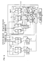
- Fig. 1 is a block diagram showing an example of a buffer storage apparatus of the type in which both the TLB and BAA systems are referred to in parallel.
- a virtual address is loaded in a register 1a.
- Entries of a TLB 2 are identified by the lower bits of the page address of the virtual address.
- the TLB 2 is constructed of k columns ⁇ 2 rows, including a first row 2-1 and a second row 2-2. Namely, each of the first and second rows has k entries.
- Each entry of the rows 2-1 and 2-2 of the TLB 2 is constructed of a virtual or logical address part (L), a valid flag bit part (V) and a real address part (R).
- L virtual or logical address part
- V valid flag bit part
- R real address part
- the entries of the BAA are identified by the upper bits of the intra-page address.
- a BAA 3 is constructed of l columns ⁇ 2 rows, including a first row 3-1 and a second row 3-2. Each row has l entries.
- the number l of columns of the BAA is decided based on the block size of the buffer storage. Namely, assuming that the page size is 4 KB and the block size is 64 bytes, the number l of columns is 64. The number of rows is decided by the buffer storage capacity.
- Each entry of the BAA 3 is constructed of a real address part (R) and a valid flag bit part (V).
- Real address comparators 6-1 and 6-2 compare the contents of the R parts of the BAA 3-1 and 3-2 with a real address (page address) read from the R part of the TLB 2-1 inputted to a selector 5 or a real address (page address) directly loaded from the central processing unit into the register 1a.
- the selector 5 selects the content of the register 1a when the central processing unit has directly loaded a real address in the register 1a, or selects the content of the TLB 2-1 when a virtual address has been loaded in the register 1a.
- Other real address comparators 7-1 and 7-2 compare real addresses read from the R parts of the TLB 2-2 with real addresses read from the R parts of the BAA 3-1 and 3-2.
- Each of the real address comparators 6-1, 6-2, 7-1 and 7-2 outputs "1" when two inputs become coincident.
- the comparison results by the real address comparators 6-1, 6-2, 7-1 and 7-2 are inputted to an encoder 8 and selected based on the results of the virtual address comparators 4-1 and 4-2 and thereafter, the encoded output (one bit in this case) is stored in a register 9 at its upper portion and the intra-page address in the register 1a at its lower portion.
- a buffer storage address corresponding to a virtual address or a real address loaded in the register 1a can be obtained in the register 9.
- the buffer storage is accessed and the read-out data is transferred to the central processing unit.
- the TLB 2 and BAA 3 must operate at high speed and also must have a certain capacity. Accordingly, they are commonly constructed of bipolar memories. A conventional bipolar memory used for such application is shown in Fig. 6.
- address signals applied to input pins A0 to A2 and A3 to A5 are decoded by an X address decoder 10 and a Y address decoder 14, respectively, and supplied to drivers 11 and 13 which in turn activate a memory cell 12.
- the memory cell 12 is constructed of 64 bits of 8 bits ⁇ 8 bits.
- One bit selected from the memory cell 12 is supplied to an output circuit 16 via a sense amplifier 15 to thereby output read-out data at an output pin DO (data out). While a WE (write enable) signal is valid, a write mode is activated.
- the bipolar memory of this type is used as the TLB or BAA by arranging it in matrix configuration realizing a desired word length and bit width.
- the Japanese Patent Publication JP-B-57-57784 discloses the apparatus which uses a TLB and a BAA constructed of a memory chip with a comparator included therein.
- the above described restriction is intended to be solved by including in a memory chip the portion encircled by a broken line in Fig. 1, for example.
- U.S. Patent 4,332,010 also discloses a memory chip with a comparator included therein.
- a real address read from a TLB is temporarily outputted from the memory chip having the TLB and inputted to a memory chip having a BAA to be compared with a real address read by the BAA. Therefore, there is a problem that the number of pins necessary for the input/output with respect to the TLB and BAA, and a propagation delay are increased.
- the integrated logic-in memory device comprises, in an integrated circuit form, first memory for holding a real address part of a TLB, a second memory for holding a real address part of a BAA, and at least a comparator for comparing an output from the first memory with an output from the second memory.
- a real address is not transferred from a TLB chip to a BAA chip so that it is possible to decrease the number of pins and a propagation delay.
- the TLB and the BAA each take over a different function, they operate in close relationship to each other so that they may be implemented in a single chip. However, it is not practical in some cases since the resultant chip becomes large.
- the TLB is divided such that the portion holding a real address part is implemented in a single chip together with the BAA.
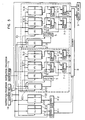
- Fig. 3 is a block diagram illustrating an embodi ment of the present invention.
- the portion encircled by a broken line in Fig. 3 is a memory chip constituting a gist of the present invention. Similar constituent elements to those in Fig. 1 are represented by using identical numbers.
- the memory chip encircled by a broken line includes rows 3-1 and 3-2 constituting a BAA 3, comparators 6-1, 6-2, 7-1 and 7-2, R parts 2-13 and 2-23 of the rows which in part constitute a TLB 2, and a selector 5. Rows 3-1 and 3-2 of the BAA are connected to a common input for a column address, i.e., to upper bits of the intrapage address in an address register 1a.
- R parts 2-13 and 2-23 of the TLB are connected to a common input for a column address different from that of the BAA, i.e., to lower bits of the page address in the address register 1a.
- Rows 3-1 and 3-2 of the BAA and R parts 2-13 and 2-23 of the TLB are connected to a common data-in signal input, i.e., to a register 1b for address registration.
- a V part of the BAA is used as an enable signal for the comparators.
- L and V parts of the TLB and comparators 4-1 and 4-2 may be implemented as another memory chip with the comparators included therein.
- Fig. 4 is a particular circuit diagram of the memory chip encircled by a broken line in Fig. 3.
- numbers in parentheses represent the number of signals which changes as the degree of integration changes, and the present invention is not intended to be limited to such numbers.
- Reference numbers 20-1 and 20-2 represent a first memory constructed of two rows in this embodiment
- 20-3 and 20-4 represent a second memory constructed of two rows in this embodiment.
- the internal structure of the memory parts 20-1 to 20-4 may be similar to that of a conventional one.
- the memory parts 20-1 to 20-4 are supplied with corresponding write enable (WE) signals 24-1 and a common data-in signal 26.
- WE write enable
- the memory parts 20-1 and 20-2 are supplied with a common first address signal 25-1a, and the memory parts 20-3 and 20-4 are supplied with a common second address signal 25-2. Accordingly, data-out signals 30-1 to 30-4 are outputted from the memory parts.
- a selector 23 selects the data-out signal 30-1 or one of the address signals 25-1a and 25-1b based on a data select signal 27 to thereby deliver it as an output signal 28.
- Comparators 21-1 to 21-4 compare the data-out signals 30-3 and 30-4 read from the memory parts 20-3 and 20-4 with the output signal 28 from the selector 23 and the output signal 30-2 from the memory part 30-2.
- the comparators 20-3 to 20-4 each output a comparison output "1" signal 29-1 to 29-4 when two inputs to each comparator are not coincident.
- the memory parts 20-1 to 20-4 are substantially similar to those conventional ones. However, according to the aspect of the present invention, the memory parts are divided into the first and second memories, and the outputs of the first and second memories are compared with each other. The operation at each mode will be described:
- the contents of the data-in signal 26 are written to the memory part designated by the write enable signal at an address designated by the address signal 25-1a or 25-2.
- the memory parts 20-1 and 20-2 correspond to the first and second rows of the real address parts of the TLB, while the memory parts 20-3 and 20-4 correspond to the first and second rows of the BAA.
- a new address is registered in the TLB or BAA after a specific row has been selected in accordance with a particular algorithm. Since the registration of an address into the TLB and BAA is not performed at the same time in ordinary case, a data-in signal can be supplied in a similar manner for all the memory parts so that the number of package pins can be advantageously decreased.
- the address signals 25-1a and 25-2 are made valid to activate the memory parts 20-1 to 20-4 and output the data-out signals.
- the data-out signal 30-1 is selected based on the data select signal 27 and outputted as the output signal 28.
- the output signal 28 is supplied to the comparators 21-1 and 21-2, while the data-out signals 30-2 to 30-4 are supplied to the comparators 21-1 to 21-4.
- the comparator 21-1 compares the first row of the real address part of the TLB with the first row of the real address part of the BAA
- the comparator 21-2 compares the first row of the real address part of the TLB with the second row of the real address part of the BAA
- the comparator 21-3 compares the second row of the real address part of the TLB with the first row of the real address part of the BAA
- the comparator 21-4 compares the second row of the real address part of the TLB with the second row of the real address part of the BAA.
- the comparison results are outputted as the outputs 29-1 to 29-4.
- the comparators 21-1 to 21-4 each make its outputs 29-1 to 29-4 "1" when two input bits to each comparator are not coincident, by means of an exclusive OR operation.
- comparators 21-1 to 21-4 may be constructed such that the outputs 29-1 to 29-4 may be made "1" when two input bits become coincident.
- the selector 23 selects the real address part of the TLB when the address referring to the BAA is a virtual address, and selects the address itself referring to the BAA when it is a real address.
- the signals 24-1 to 24-4, 25-1a and 25-1b, 25-2, 26, 27, 29-1 to 29-4 are inputted from or outputted to corresponding input or output pins provided on the package.
- Fig. 5 is a block diagram showing another embodiment of the present invention, which uses two memory chips in contrast with one memory chip in the embodiment of Fig. 3.
- the number of rows used in the embodiment of Fig. 3 is 2.
- This embodiment shown in Fig. 5 is effective in the case where the number of rows are large so that the Fig. 3 embodiment cannot accommodate such rows.
- Memory chips 100 and 101 have quite the same structure as that shown in Fig. 3.
- R parts 2-13 and 2-13′ in the memory chips 100 and 101 are the first row of the TLB and stores the same real address.
- R parts 2-23 and 2-23′ in the memory chips 100 and 101 are the second row of the TLB and stores the same real address.
- Reference numbers 3-1 and 3-2 in the memory chip 100 represent first and second rows 1 and 2 of the BAA, respectively, while reference numbers 3-3 and 3-4 in the memory chip 101 represent third and fourth rows of the BAA, respectively.
- Fig. 6 shows another embodiment of this invention, wherein two memory chips 200 and 201 are used similar to the embodiment of Fig. 5.
- This embodiment is useful in the case where each memory chip has insufficient bit capacity. For example, if one memory part shown as having 8-bit length in Fig. 4 has 4 bit length or a real address of 16 bits is required to be loaded, the upper and lower halves of an address is divisionally loaded in the memory chips 200 and 201.
- Each row of the BAA has a V part, whereas a row 3-1a serving to handle the upper bits of the same row has not a V part and row 3-1b (in the memory chip 201) serving to handle the lower bits has a V part.
- An encoder 80 judges the coincidence of a row when the upper and lower bits both become coincident.
- the R part of the TLB has been described as not having the V part.
- the V part may be added to the R part such that the V part set at "1" is compared with a corresponding V part of the BAA at the comparator.
- the comparator may be constructed such that the bit corresponding to the V part of the BAA is fixed to a high level.
- L and V parts of the TLB have been disposed outside of the memory chip in the above embodiments, various discriminators, table origins (STO) or storage protection keys may be stored in the memory chip.
- STO table origins
- a column address of the BAA not only the upper bits of the intra-page address but also the lower address of the page address may be used.
- the lower bits of the TLB column address in the memory chip and the upper bits of the BAA column address are duplicated so that ones of these bits may be shared in use.
- the memory parts for the real addresses of the TLB and BAA and the comparator section for comparing the outputs of the memory parts are mounted on the same memory package. Therefore, propagation delay and the number of pins are effectively decreased.
- the register 1a for loading an address accessing to the TLB and BAA and the register 1b for loading a real address to be registered in the TLB and BAA are separately constructed.
- the registers 1a and 1b may be combined as a common register.
Landscapes
- Engineering & Computer Science (AREA)
- Theoretical Computer Science (AREA)
- Physics & Mathematics (AREA)
- General Engineering & Computer Science (AREA)
- General Physics & Mathematics (AREA)
- Memory System Of A Hierarchy Structure (AREA)
Applications Claiming Priority (2)
| Application Number | Priority Date | Filing Date | Title |
|---|---|---|---|
| JP61247414A JPH0661066B2 (ja) | 1986-10-20 | 1986-10-20 | 記憶制御装置 |
| JP247414/86 | 1986-10-20 |
Publications (3)
| Publication Number | Publication Date |
|---|---|
| EP0264912A2 true EP0264912A2 (fr) | 1988-04-27 |
| EP0264912A3 EP0264912A3 (en) | 1990-02-14 |
| EP0264912B1 EP0264912B1 (fr) | 1994-01-05 |
Family
ID=17163078
Family Applications (1)
| Application Number | Title | Priority Date | Filing Date |
|---|---|---|---|
| EP87115348A Expired - Lifetime EP0264912B1 (fr) | 1986-10-20 | 1987-10-20 | Système de commande de mémoire et dispositif de mémoire à logique incorporée |
Country Status (5)
| Country | Link |
|---|---|
| US (1) | US4943914A (fr) |
| EP (1) | EP0264912B1 (fr) |
| JP (1) | JPH0661066B2 (fr) |
| KR (1) | KR910001737B1 (fr) |
| DE (1) | DE3788704T2 (fr) |
Cited By (2)
| Publication number | Priority date | Publication date | Assignee | Title |
|---|---|---|---|---|
| EP0311034A3 (en) * | 1987-10-07 | 1990-07-04 | Hitachi, Ltd. | Cache memory control apparatus for a virtual memory data-processing system |
| EP0549321A3 (en) * | 1991-12-27 | 1993-09-08 | Texas Instruments Incorporated | Method and system for high-speed virtual-to-physical address translation and cache tag matching |
Families Citing this family (15)
| Publication number | Priority date | Publication date | Assignee | Title |
|---|---|---|---|---|
| KR920001282B1 (ko) * | 1987-10-02 | 1992-02-10 | 가부시키가이샤 히타치세이사쿠쇼 | 버퍼메모리 제어장치 |
| US5293612A (en) * | 1989-05-11 | 1994-03-08 | Tandem Computers Incorporated | Selective dump method and apparatus |
| JPH035851A (ja) * | 1989-06-01 | 1991-01-11 | Fujitsu Ltd | バッファ記憶装置 |
| JPH0748191B2 (ja) * | 1989-08-10 | 1995-05-24 | 株式会社日立製作所 | バッファ記憶制御装置 |
| JPH03216744A (ja) * | 1990-01-22 | 1991-09-24 | Fujitsu Ltd | 内蔵キャッシュ・メモリ制御方式 |
| US5584003A (en) * | 1990-03-29 | 1996-12-10 | Matsushita Electric Industrial Co., Ltd. | Control systems having an address conversion device for controlling a cache memory and a cache tag memory |
| GB2246001B (en) * | 1990-04-11 | 1994-06-15 | Digital Equipment Corp | Array architecture for high speed cache memory |
| US5498990A (en) * | 1991-11-05 | 1996-03-12 | Monolithic System Technology, Inc. | Reduced CMOS-swing clamping circuit for bus lines |
| US5576554A (en) * | 1991-11-05 | 1996-11-19 | Monolithic System Technology, Inc. | Wafer-scale integrated circuit interconnect structure architecture |
| EP0541288B1 (fr) * | 1991-11-05 | 1998-07-08 | Fu-Chieh Hsu | Architecture à redondance pour module de circuit |
| US5831467A (en) * | 1991-11-05 | 1998-11-03 | Monolithic System Technology, Inc. | Termination circuit with power-down mode for use in circuit module architecture |
| DE69331061T2 (de) * | 1992-08-10 | 2002-06-06 | Monolithic System Tech Inc | Fehlertolerantes hierarchisiertes Bussystem |
| US5604889A (en) * | 1994-06-15 | 1997-02-18 | Texas Instruments Incorporated | Memory management system for checkpointed logic simulator with increased locality of data |
| US5655113A (en) | 1994-07-05 | 1997-08-05 | Monolithic System Technology, Inc. | Resynchronization circuit for a memory system and method of operating same |
| JP3456768B2 (ja) * | 1994-09-28 | 2003-10-14 | 株式会社東芝 | アドレス変換装置 |
Family Cites Families (5)
| Publication number | Priority date | Publication date | Assignee | Title |
|---|---|---|---|---|
| US4317168A (en) * | 1979-11-23 | 1982-02-23 | International Business Machines Corporation | Cache organization enabling concurrent line castout and line fetch transfers with main storage |
| US4332010A (en) * | 1980-03-17 | 1982-05-25 | International Business Machines Corporation | Cache synonym detection and handling mechanism |
| US4400770A (en) * | 1980-11-10 | 1983-08-23 | International Business Machines Corporation | Cache synonym detection and handling means |
| US4695950A (en) * | 1984-09-17 | 1987-09-22 | International Business Machines Corporation | Fast two-level dynamic address translation method and means |
| CA1272301A (fr) * | 1985-02-22 | 1990-07-31 | Howard Gene Sachs | Systeme de gestion d'antememoire et de memoire |
-
1986
- 1986-10-20 JP JP61247414A patent/JPH0661066B2/ja not_active Expired - Lifetime
-
1987
- 1987-10-19 KR KR8711559A patent/KR910001737B1/ko not_active Expired
- 1987-10-20 DE DE3788704T patent/DE3788704T2/de not_active Expired - Fee Related
- 1987-10-20 EP EP87115348A patent/EP0264912B1/fr not_active Expired - Lifetime
- 1987-10-20 US US07/110,425 patent/US4943914A/en not_active Expired - Lifetime
Cited By (2)
| Publication number | Priority date | Publication date | Assignee | Title |
|---|---|---|---|---|
| EP0311034A3 (en) * | 1987-10-07 | 1990-07-04 | Hitachi, Ltd. | Cache memory control apparatus for a virtual memory data-processing system |
| EP0549321A3 (en) * | 1991-12-27 | 1993-09-08 | Texas Instruments Incorporated | Method and system for high-speed virtual-to-physical address translation and cache tag matching |
Also Published As
| Publication number | Publication date |
|---|---|
| DE3788704D1 (de) | 1994-02-17 |
| DE3788704T2 (de) | 1994-05-19 |
| KR880005518A (ko) | 1988-06-29 |
| EP0264912A3 (en) | 1990-02-14 |
| JPH0661066B2 (ja) | 1994-08-10 |
| JPS63101944A (ja) | 1988-05-06 |
| KR910001737B1 (en) | 1991-03-22 |
| US4943914A (en) | 1990-07-24 |
| EP0264912B1 (fr) | 1994-01-05 |
Similar Documents
| Publication | Publication Date | Title |
|---|---|---|
| EP0264912B1 (fr) | Système de commande de mémoire et dispositif de mémoire à logique incorporée | |
| US5526509A (en) | Method and apparatus for controlling one or more hierarchical memories using a virtual storage scheme and physical to virtual address translation | |
| US3761881A (en) | Translation storage scheme for virtual memory system | |
| US4654781A (en) | Byte addressable memory for variable length instructions and data | |
| KR950007448B1 (ko) | 집적회로 메모리 시스템 | |
| US5752260A (en) | High-speed, multiple-port, interleaved cache with arbitration of multiple access addresses | |
| US4589092A (en) | Data buffer having separate lock bit storage array | |
| US4507731A (en) | Bidirectional data byte aligner | |
| US5040153A (en) | Addressing multiple types of memory devices | |
| US4899272A (en) | Addressing multiple types of memory devices | |
| US5053951A (en) | Segment descriptor unit for performing static and dynamic address translation operations | |
| US6141287A (en) | Memory architecture with multilevel hierarchy | |
| EP0311034B1 (fr) | Dispositif de commande d'une mémoire cache pour un système de traitement de données à mémoire virtuelle | |
| JPH0594698A (ja) | 半導体記憶装置 | |
| US5276850A (en) | Information processing apparatus with cache memory and a processor which generates a data block address and a plurality of data subblock addresses simultaneously | |
| US5544340A (en) | Method and system for controlling cache memory with a storage buffer to increase throughput of a write operation to the cache memory | |
| US5742790A (en) | Detection circuit for identical and simultaneous access in a parallel processor system with a multi-way multi-port cache | |
| JPH0438014B2 (fr) | ||
| US5396605A (en) | Buffer storage control apparatus including a translation lookaside buffer and an improved address comparator layout arrangement | |
| GB2117945A (en) | Memory data transfer | |
| EP0376253B1 (fr) | Appareil de traitement d'information avec antémémoire | |
| KR920003845B1 (ko) | 개인용 컴퓨터의 사용자를 위한 rom의 영역 확장 시스템 | |
| WO1988009014A2 (fr) | Systeme d'adressage de memoire | |
| JP2595753B2 (ja) | キャッシュメモリの無効化方式 | |
| JP2542284B2 (ja) | 緩衝記憶装置および緩衝記憶装置システム |
Legal Events
| Date | Code | Title | Description |
|---|---|---|---|
| PUAI | Public reference made under article 153(3) epc to a published international application that has entered the european phase |
Free format text: ORIGINAL CODE: 0009012 |
|
| AK | Designated contracting states |
Kind code of ref document: A2 Designated state(s): DE FR GB |
|
| PUAL | Search report despatched |
Free format text: ORIGINAL CODE: 0009013 |
|
| AK | Designated contracting states |
Kind code of ref document: A3 Designated state(s): DE FR GB |
|
| 17P | Request for examination filed |
Effective date: 19900216 |
|
| 17Q | First examination report despatched |
Effective date: 19930208 |
|
| GRAA | (expected) grant |
Free format text: ORIGINAL CODE: 0009210 |
|
| AK | Designated contracting states |
Kind code of ref document: B1 Designated state(s): DE FR GB |
|
| REF | Corresponds to: |
Ref document number: 3788704 Country of ref document: DE Date of ref document: 19940217 |
|
| ET | Fr: translation filed | ||
| PLBE | No opposition filed within time limit |
Free format text: ORIGINAL CODE: 0009261 |
|
| STAA | Information on the status of an ep patent application or granted ep patent |
Free format text: STATUS: NO OPPOSITION FILED WITHIN TIME LIMIT |
|
| 26N | No opposition filed | ||
| PGFP | Annual fee paid to national office [announced via postgrant information from national office to epo] |
Ref country code: FR Payment date: 20010830 Year of fee payment: 15 |
|
| PGFP | Annual fee paid to national office [announced via postgrant information from national office to epo] |
Ref country code: GB Payment date: 20011010 Year of fee payment: 15 |
|
| PGFP | Annual fee paid to national office [announced via postgrant information from national office to epo] |
Ref country code: DE Payment date: 20011228 Year of fee payment: 15 |
|
| REG | Reference to a national code |
Ref country code: GB Ref legal event code: IF02 |
|
| PG25 | Lapsed in a contracting state [announced via postgrant information from national office to epo] |
Ref country code: GB Free format text: LAPSE BECAUSE OF NON-PAYMENT OF DUE FEES Effective date: 20021020 |
|
| PG25 | Lapsed in a contracting state [announced via postgrant information from national office to epo] |
Ref country code: DE Free format text: LAPSE BECAUSE OF NON-PAYMENT OF DUE FEES Effective date: 20030501 |
|
| GBPC | Gb: european patent ceased through non-payment of renewal fee |
Effective date: 20021020 |
|
| PG25 | Lapsed in a contracting state [announced via postgrant information from national office to epo] |
Ref country code: FR Free format text: LAPSE BECAUSE OF NON-PAYMENT OF DUE FEES Effective date: 20030630 |
|
| REG | Reference to a national code |
Ref country code: FR Ref legal event code: ST |