EP0267555A2 - Spektrometerobjektiv für Korpuskularstrahlmessgeräte und Verfahren zur Untersuchung von Proben. - Google Patents
Spektrometerobjektiv für Korpuskularstrahlmessgeräte und Verfahren zur Untersuchung von Proben. Download PDFInfo
- Publication number
- EP0267555A2 EP0267555A2 EP87116416A EP87116416A EP0267555A2 EP 0267555 A2 EP0267555 A2 EP 0267555A2 EP 87116416 A EP87116416 A EP 87116416A EP 87116416 A EP87116416 A EP 87116416A EP 0267555 A2 EP0267555 A2 EP 0267555A2
- Authority
- EP
- European Patent Office
- Prior art keywords
- spectrometer
- electrode
- objective lens
- objective
- potential
- Prior art date
- Legal status (The legal status is an assumption and is not a legal conclusion. Google has not performed a legal analysis and makes no representation as to the accuracy of the status listed.)
- Granted
Links
Images


Classifications
-
- H—ELECTRICITY
- H01—ELECTRIC ELEMENTS
- H01J—ELECTRIC DISCHARGE TUBES OR DISCHARGE LAMPS
- H01J37/00—Discharge tubes with provision for introducing objects or material to be exposed to the discharge, e.g. for the purpose of examination or processing thereof
- H01J37/02—Details
- H01J37/04—Arrangements of electrodes and associated parts for generating or controlling the discharge, e.g. electron-optical arrangement or ion-optical arrangement
- H01J37/10—Lenses
- H01J37/14—Lenses magnetic
-
- H—ELECTRICITY
- H01—ELECTRIC ELEMENTS
- H01J—ELECTRIC DISCHARGE TUBES OR DISCHARGE LAMPS
- H01J37/00—Discharge tubes with provision for introducing objects or material to be exposed to the discharge, e.g. for the purpose of examination or processing thereof
- H01J37/02—Details
- H01J37/04—Arrangements of electrodes and associated parts for generating or controlling the discharge, e.g. electron-optical arrangement or ion-optical arrangement
- H01J37/05—Electron or ion-optical arrangements for separating electrons or ions according to their energy or mass
-
- H—ELECTRICITY
- H01—ELECTRIC ELEMENTS
- H01J—ELECTRIC DISCHARGE TUBES OR DISCHARGE LAMPS
- H01J37/00—Discharge tubes with provision for introducing objects or material to be exposed to the discharge, e.g. for the purpose of examination or processing thereof
- H01J37/02—Details
- H01J37/244—Detectors; Associated components or circuits therefor
-
- H—ELECTRICITY
- H01—ELECTRIC ELEMENTS
- H01J—ELECTRIC DISCHARGE TUBES OR DISCHARGE LAMPS
- H01J37/00—Discharge tubes with provision for introducing objects or material to be exposed to the discharge, e.g. for the purpose of examination or processing thereof
- H01J37/26—Electron or ion microscopes; Electron or ion diffraction tubes
- H01J37/266—Measurement of magnetic or electric fields in the object; Lorentzmicroscopy
- H01J37/268—Measurement of magnetic or electric fields in the object; Lorentzmicroscopy with scanning beams
-
- H—ELECTRICITY
- H01—ELECTRIC ELEMENTS
- H01J—ELECTRIC DISCHARGE TUBES OR DISCHARGE LAMPS
- H01J2237/00—Discharge tubes exposing object to beam, e.g. for analysis treatment, etching, imaging
- H01J2237/05—Arrangements for energy or mass analysis
- H01J2237/057—Energy or mass filtering
-
- H—ELECTRICITY
- H01—ELECTRIC ELEMENTS
- H01J—ELECTRIC DISCHARGE TUBES OR DISCHARGE LAMPS
- H01J2237/00—Discharge tubes exposing object to beam, e.g. for analysis treatment, etching, imaging
- H01J2237/244—Detection characterized by the detecting means
- H01J2237/2448—Secondary particle detectors
-
- H—ELECTRICITY
- H01—ELECTRIC ELEMENTS
- H01J—ELECTRIC DISCHARGE TUBES OR DISCHARGE LAMPS
- H01J2237/00—Discharge tubes exposing object to beam, e.g. for analysis treatment, etching, imaging
- H01J2237/244—Detection characterized by the detecting means
- H01J2237/2449—Detector devices with moving charges in electric or magnetic fields
-
- H—ELECTRICITY
- H01—ELECTRIC ELEMENTS
- H01J—ELECTRIC DISCHARGE TUBES OR DISCHARGE LAMPS
- H01J2237/00—Discharge tubes exposing object to beam, e.g. for analysis treatment, etching, imaging
- H01J2237/245—Detection characterised by the variable being measured
- H01J2237/24507—Intensity, dose or other characteristics of particle beams or electromagnetic radiation
-
- H—ELECTRICITY
- H01—ELECTRIC ELEMENTS
- H01J—ELECTRIC DISCHARGE TUBES OR DISCHARGE LAMPS
- H01J2237/00—Discharge tubes exposing object to beam, e.g. for analysis treatment, etching, imaging
- H01J2237/245—Detection characterised by the variable being measured
- H01J2237/24571—Measurements of non-electric or non-magnetic variables
- H01J2237/24585—Other variables, e.g. energy, mass, velocity, time, temperature
Definitions
- the invention relates to a spectrometer lens for corpuscular beam measuring devices according to the preamble of patent claim 1.
- Such a spectrometer lens is from the publication by E. Plies "A new objective lens with in-lens spectrometer for electron beam testing", Proc. XIth Int. Cong. on Electron Microscopy, Kyoto, August 31 - September 7, 1986, pages 625-626.
- This spectrometer objective which essentially consists of a short focal length magnetic objective lens, a deflection unit arranged inside the objective lens and an electrostatic counterfield spectrometer, forms the component of the electron-optical column of an electron beam measuring device with which both the primary electrons emitted by a high-current electron source and the secondary electrons released on a sample be focused into a point on the optical axis of the system.
- the focus of the secondary electrons which are accelerated to high kinetic energies, lies in the center of a spherically symmetrical opposing field, which is generated in a spectrometer part arranged above the objective lens with the aid of an appropriately designed pair of electrodes.
- a spherically symmetrical opposing field which is generated in a spectrometer part arranged above the objective lens with the aid of an appropriately designed pair of electrodes.
- one is forced to place the suction electrode arranged directly above the sample at a high positive potential.
- High suction fields E ⁇ 1 to 2 kV / mm
- disturbances in the homogeneity of the suction field as they occur in particular in the case of strongly structured samples, have an unfavorable effect on the spatial resolution ( ⁇ diameter of the electron probe on the sample) of the electron beam measuring device.
- the invention has for its object to provide a spectrometer lens of the type mentioned, the imaging properties of which are not influenced by the structure of the sample examined. In addition, damage to the sample from high suction fields should be avoided.
- the advantage that can be achieved with the invention is, in particular, that even highly structured samples, in particular highly integrated circuits on semiconductor wafers, can be examined in a corpuscular beam measuring device with high spatial resolution.
- Claims 2 to 15 are directed to preferred refinements and developments of the invention.
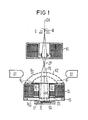
- the spectrometer objective shown schematically in FIGS. 1 and 2 essentially consists of a short focal length, largely asymmetrical objective lens OL, a single-stage deflection system DS arranged symmetrically to the optical axis OA within the magnetic lens OL and an electrostatic counterfield spectrometer which has an electrode arrangement SG, G1 for acceleration which has secondary electrons SE triggered on a sample IC, preferably in the integrated circuit, and an electrode pair K1 / K2 which generates a spherically symmetrical opposing field.
- the system consisting of objective lens OL, deflection unit DS and spectrometer forms the component of the electron-optical column shown schematically in FIG.
- the electron source Q or its intermediate image ZP generated by condenser lenses KL is reduced with the aid of the spectrometer lens to the sample arranged in the immediate vicinity of the rear focal plane of the magnetic lens OL IC off.
- the positioning of the primary electron beam PE on a point of the sample IC, which is not described in more detail, or its line-shaped deflection is carried out with the aid of the deflection unit DS.
- the electrode arrangement for extracting and accelerating the secondary electrons SE consists of a flat electrode SG arranged in the beam path directly above the sample IC and a grid electrode G1 arranged in the region of the lower pole piece of the objective lens OL, which preferably has a high positive potential V E of about 1 to 5 kV is.
- the electrode SG which is insulated on the lower pole piece or within the pole piece gap, is supplied with a potential V SG between the sample potential (normally earth potential) and the potential V E of the electrode G1, in particular with a potential between 0 and 100 volts, that the field strength in the area of the sample IC remains below a critical value. In addition, it is ensured that unevenness of the sample surface has no influence on the homogeneity of the electrical field built up between the electrodes SG and G1.
- the lower electrode SG is preferably designed as a grid and has one by insulators IS lower pole piece of the objective lens OL separate annular holder part which is conductively connected to a variable voltage source. Instead of the grid electrode G1, a pinhole can of course also be used.
- the accelerated secondary electrons SE pass through the grid electrode G1 and enter the magnetic field of the objective lens OL between the pole pieces by focusing them in a point ZS lying on the optical axis OA.
- the position of this focusing point ZS which is to be interpreted as a real intermediate image of the virtual source below the sample IC (smallest caustic cross-section of all virtual secondary electron tracks below the sample IC) of the secondary electrons SE, is determined here by the height of the potential V E applied to the grid electrode G1 and the magnetic field strength in the pole shoe gap, which is dependent on the primary electron energy.
- the braking and the energy analysis of the secondary electrons SE takes place within or, as shown in FIGS. 1 and 2, above the objective lens OL in a spherically symmetrical electrical opposing field, that one lies in the space between two almost hemispherical, at different potentials V E and V G
- Grid electrodes K1 and K2 builds. While the lower grid electrode K1 is at the potential V E of the electrode G1, the upper grid electrode K2 is usually supplied with potentials between approximately -15 volts and +15 volts. Above the electrode arrangement K1 building up the opposing field, 1 and 2, the potential of which is preferably chosen to be equal to the potential V G of the electrode K2.
- the secondary electron focus ZS should be sufficiently far above the pole pieces and the deflection unit DS.
- the focusing of the secondary electrons in a point ZS of the optical axis OA lying above the deflection unit DS is possible the better the smaller the energy of the primary electrons PE and the higher the potential V E of the electrode G1 chosen to accelerate the secondary electrons SE.
- the grid electrode K1 is conductively connected to the electrode G1 via a hollow cylinder HZ arranged concentrically to the optical axis OA.
- the spectrometer objective shown in Fig. 3 consists essentially of a short focal length objective lens OL, a deflection unit DS arranged symmetrically to the optical axis OA within the objective lens OL and an electrostatic counterfield spectrometer which the electrode arrangement SG / G1 known from FIGS. 1 and 2 for suction and Accelerate the secondary electrons SE and has an electrode arrangement K1 / K2 that generates a spherically symmetrical opposing field.
- the system consisting of objective lens OL, deflection unit DS and counter-field spectrometer forms the component of the electron-optical column of an electron beam measuring device with which the primary electrons PE emitted by a high-current electron source are focused and deflected and the secondary electrons SE triggered on the sample IC are preferably in the one on the optical axis OA Center ZS of the spherically symmetrical opposing field can be focused.
- This opposing field is generated with the aid of the grid electrodes K1 and K2 arranged in a housing GH above the objective lens OL, each forming parts of the surface of concentric spheres with different radii R1 or R2 (R1 ⁇ 30 mm, R2 ⁇ 34 mm).
- the center point ZS defining the center of the opposing field of the balls assigned to the grid electrodes K1 and K2 lies very far above the deflection unit DS, which preferably consists of magnetic and electrical deflection elements MD or ED, and the pole shoe gap, lamella rotations of the secondary electrons SE become after passing through the intermediate image ZS avoided.
- the housing GH which is closed off by a ring-shaped secondary electron detector DT, in which, in addition to the electrodes K1 and K2, there is also a shielding grid BG and a channel plate CP or a semiconductor detector for detecting the secondary electrons SE are provided, a hollow cylinder HZ consisting of three parts, arranged symmetrically to the optical axis OA.
- this hollow cylinder HZ which tapers in the region of the objective lens OL, is conductively connected to the electrode K1 which is at a potential V E
- the lower part thereof Partly terminated on the sample side by the electrode G1, which is also at the potential V E between approximately 0.5 and 5 kV, in particular 2 kV.
- the central cylinder part surrounded by the magnetic deflection element MD is designed here as in the known spectrometer objective according to E. Plies as an electrostatic eight-pole deflector ED, the individual electrodes of which are acted upon by a further potential V X for deflecting the primary beam.
- the STigmator ST for compensation of the axial astigmatism can be dispensed with if the electrodes of the eight-pole deflector ED are provided with suitable additional voltages.
- the homogeneous electric and magnetic fields generated with the aid of the deflection unit DS are spatially oriented to one another in the manner of a Wien filter in such a way that their field vectors are perpendicular to one another and in each case perpendicular to the speed vector of the secondary electrons SE.
- spectrometer lenses Due to the electrical delay field superimposed on the focusing magnetic field of the objective lens, spectrometer lenses have significantly smaller color and aperture error constants than magnetic single lenses. Since the imaging properties of such systems are largely determined by the homogeneity and the strength of the retardation field, the theoretically possible resolution limit (beam diameter on the sample) could not be reached due to the field distortion on the sample surface in conventional spectrometer objectives. The improved imaging properties only come with the decoupling of the delay field from the respective sample according to the invention of these electrostatic-magnetic lenses.
- the invention is of course not limited to the exemplary embodiments shown in FIGS. 1 to 3. It is thus possible, for example, to arrange the electrode arrangement K1, K2 generating the spherically symmetrical opposing field and possibly also the detector system completely within the objective lens OL.
- This deflection system DS can of course also be arranged in a conventional manner in the corpuscular beam path above the objective lens OL.
- This deflection system DS can of course also be arranged in a conventional manner in the corpuscular beam path above the objective lens OL.
- the lengthening of the beam path also increases the disadvantageous influence of the Boersch effect on the probe diameter.
- a flat pair of electrodes can also be used to generate the opposing field. Detection of the secondary electrons SE independent of the emission angle is no longer possible with such an arrangement.
Landscapes
- Chemical & Material Sciences (AREA)
- Analytical Chemistry (AREA)
- Analysing Materials By The Use Of Radiation (AREA)
- Electron Tubes For Measurement (AREA)
- Tests Of Electronic Circuits (AREA)
- Testing Or Measuring Of Semiconductors Or The Like (AREA)
- Other Investigation Or Analysis Of Materials By Electrical Means (AREA)
Abstract
Description
- Die Erfindung betrifft ein Spektrometerobjektiv für Korpuskularstrahlmeßgeräte nach dem Oberbegriff des Patentanspruchs 1.
- Ein solches Spektrometerobjektiv ist aus der Veröffentlichung von E. Plies "A new objective lens with in-lens spectrometer for electron beam testing", Proc. XIth Int. Cong. on Electron Microscopy, Kyoto, 31.08 - 07.09.86, Seiten 625-626 bekannt. Dieses Spektrometerobjektiv, das im wesentlichen aus einer kurzbrennweitigen magnetischen Objektivlinse, einer innerhalb der Objektivlinse angeordneten Ablenkeinheit und einem elektrostatischen Gegenfeldspektrometer besteht, bildet die Komponente der elektronenoptischen Säule eines Elektronenstrahlmeßgerätes, mit der sowohl die von einer Hochstromelektronenquelle emittierten Primärelektronen als auch die auf einer Probe ausgelösten Sekundärelektronen in einen auf der optischen Achse des Systems liegenden Punkt fokussiert werden. Der Fokus der auf hohe kinetische Energien beschleunigten Sekundärelektronen liegt hierbei im Zentrum eines kugelsymmetrischen Gegenfeldes, das man in einem oberhalb der Objektivlinse angeordneten Spektrometerteil mit Hilfe eines entsprechend ausgebildeten Elektrodenpaares erzeugt. Um eine gute Fokussierung der Sekundärelektronen zu gewährleisten ist man gezwungen, die unmittelbar oberhalb der Probe angeordnete Absaugelektrode auf ein hohes positives Potential zu legen. Hohe Absaugfelder (E ≈1 bis 2 kV/mm) im Bereich der Probe sollten aber insbesondere bei der Überprüfung der Funktionsweise mikroelektronischer Bauelemente vermieden werden. Darüberhinaus wirken sich Störungen der Homogenität des Absaugfeldes, wie sie insbesondere bei stark strukturierten Proben auftreten, ungünstig auf die Ortsauflösung ( ≈ Durchmesser der Elektronensonde auf der Probe) des Elektronenstrahlmeßgerätes aus.
- Der Erfindung liegt die Aufgabe zugrunde ein Spektrometerobjektiv der eingangs genannten Art anzugeben, dessen Abbildungseigenschaften nicht von der Struktur der untersuchten Probe beeinflußt wird. Außerdem sollen Schädigungen der Probe durch hohe Absaugfelder vermieden werden.
- Diese Aufgabe wird erfindungsgemäß durch ein Spektrometerobjektiv der eingangs genannten Art gelöst, welches die kennzeichnenden Merkmale des Patentanspruchs 1 aufweist.
- Der mit der Erfindung erzielbare Vorteil besteht insbesondere darin, daß auch stark strukturierte Proben, insbesondere hochintegrierte Schaltungen auf Halbleiterwafern, in einem Korpuskularstrahlmeßgerät mit hoher Ortsauflösung untersucht werden können.
- Die Ansprüche 2 bis 15 sind auf bevorzugte Ausgestaltungen und Weiterbildungen der Erfindung gerichtet.
- Die Erfindung wird nachfolgend anhand der Zeichnungen erläutert.
- Dabei zeigen die Fig. 1 bis 3 erfindungsgemäße Spektrometerobjektive.
- Das in den Fig. 1 und 2 schematisch dargestellte Spektrometerobjektiv besteht im wesentlichen aus einer kurzbrennweitigen, weitgehend asymmetrischen Objektivlinse OL, einem innerhalb der Magnetlinse OL symmetrisch zur optischen Achse OA angeordneten einstufigen Ablenksystem DS und einem elektrostatischen Gegenfeldspektrometer, das eine Elektrodenanordnung SG, G1 zur Beschleunigung der auf einer Probe IC, vorzugsweise in der integrierten Schaltung, ausgelösten Sekundärelektronen SE und ein ein kugelsymmetrisches Gegenfeld erzeugendes Elektrodenpaar K1/K2 aufweist. Das aus Objektivlinse OL, Ablenkeinheit DS und Spektrometer bestehende System bildet die Komponente der elektronenoptischen Säule des in Fig. 1 schematisch dargestell ten Elektronenstrahlmeßgerätes, mit der die von einem Strahlerzeuger G emittierten Primärelektronen PE fokussiert und abgelenkt und die auf der Probe IC ausgelösten Sekundärelektronen SE in einen auf der optischen Achse OA liegenden Punkt ZS abgebildet werden. Zur Erzeugung einer feinen Elektronensonde mit einem Strahlquerschnitt im Submikrometerbereich (dPE≈ 0,1 µm) bildet man die Elektronenquelle Q oder deren durch Kondensorlinsen KL erzeugtes Zwischenbild ZP mit Hilfe des Spektrometerobjektivs verkleinert auf die in unmittelbarer Nähe der hinteren Brennebene der Magnetlinse OL angeordnete Probe IC ab. Die Positionierung des Primärelektronenstrahles PE auf einem nicht näher bezeichneten Punkt der Probe IC, bzw. dessen zeilenförmige Ablenkung erfolgt mit Hilfe der Ablenkeinheit DS.
- Zum Nachweis der am Auftreffpunkt der Primärelektronen PE ausgelösten und in einem großen Raumwinkelbereich emittierten niederenergetischen Sekundärelektronen (ESE<50 eV) werden diese von der Probe IC abgesaugt und in einen homogenen elektrischen Feld in Richtung der Objektivlinse OL auf kinetische Energien zwischen etwa 1 und 5 keV beschleunigt. Erfindungsgemäß besteht die Elektrodenanordnung zum Absaugen und Beschleunigen der Sekundärelektronen SE aus einer im Strahlengang unmittelbar oberhalb der Probe IC angeordneten ebenen Elektrode SG und einer im Bereich des unteren Polschuhes der Objektivlinse OL angeordneten Gitterelektrode G1, die vorzugsweise auf hohem positiven Potential VE von etwa 1 bis 5 kV liegt. Wird die isoliert am unteren Polschuh oder innerhalb des Polschuhspaltes gehalterte Elektrode SG mit einem zwischen dem Probenpotential (normalerweise Erdpotential) und dem Potential VE der Elektrode G1 liegenden Potential VSG, insbesondere mit einem Potential zwischen 0 und 100 Volt beaufschlagt, kann man erreichen, daß die Feldstärke im Bereich der Probe IC unterhalb eines kritischen Wertes bleibt. Außerdem ist sichergestellt, das Unebenheiten der Probenoberfläche keinen Einfluß auf die Homogenität des zwischen den Elektroden SG und G1 aufgebauten elektrischen Feldes haben. Die untere Elektrode SG ist hierbei vorzugsweise als Gitter ausgebildet und weist einen durch Isolatoren IS vom unteren Polschuh der Objektivlinse OL getrennten ringförmigen Halterungsteil auf, der mit einer variablen Spannungsquelle leitend verbunden ist. Anstelle der Gitterelektrode G1 kann selbstverständlich auch eine Lochblende verwendet werden. Die beschleunigten Sekundärelektronen SE durchlaufen die Gitterelektrode G1 und gelangen in das Magnetfeld der Objektivlinse OL zwischen den Polschuhen, in dem sie in einen auf der optischen Achse OA liegenden Punkt ZS fokussiert werden. Die Lage dieses Fokussierungspunktes ZS, der als reelles Zwischenbild der unterhalb der Probe IC liegenden virtuellen Quelle (kleinster Kaustikquerschnitt aller virtuellen Sekundärelektronenbahnen unterhalb der Probe IC) der Sekundärelektronen SE zu interpretieren ist, wird hierbei von der Höhe des an der Gitterelektrode G1 anliegenden Potentials VE und der von der Primärelektronenenergie abhängigen Magnetfeldstärke im Polschuhspalt bestimmt. Eine gute Fokussierung der Sekundärelektronen SE im Feld der Objektivlinse OL ist erst durch deren Beschleunigung auf hohe kinetische Energien (ESE = 1 bis 5 KeV) gewährleistet, da nur dann die Bildweiten der am Meßpunkt mit unterschiedlichen Energien (0 < E₀ < 50 eV) emittierten Sekundärelektronen SE nahezu gleich sind. Da die Primärelektronen PE die Objektivlinse OL bei hohen Beschleunigungspotentialen VE ebenfalls mit hoher Energie durchlaufen, wird auch der nachteilige Einfluß des Boersch-Effektes (Coulomb-Wechselwirkung der Elektronen im Primärstrahl) auf den Sondendurchmesser in diesem Teil des elektronenoptischen Strahlengangs reduziert.
- Die Abbremsung und die Energieanalyse der Sekundärelektronen SE erfolgt innerhalb, oder wie in Fig. 1 und 2 dargestellt, oberhalb der Objektivlinse OL in einem kugelsymmetrischen elektrischen Gegenfeld, daß man im Raumbereich zwischen zwei nahezu halbkugelförmigen, auf unterschiedlichem Potential VE bzw. VG liegenden Gitterelektroden K1 und K2 aufbaut. Während die untere Gitterelektrode K1 auf dem Potential VE der Elektrode G1 liegt, wird die obere Gitterelektrode K2 üblicherweise mit Potentialen zwischen etwa -15 Volt und +15 Volt beaufschlagt. Oberhalb der das Gegenfeld aufbauenden Elektrodenanordnung K1, K2 kann noch eine in den Fig. 1 und 2 nicht dargestellte Abschirmelektrode vorgesehen sein, deren Potential vorzugsweise gleich dem Potential VG der Elektrode K2 gewählt wird.
- Um Lamordrehungen der Sekundärelektronen SE innerhalb der Objektivlinse OL zu vermeiden, sollte der Sekundärelektronenfokus ZS genügend weit oberhalb der Polschuhe und der Ablenkeinheit DS liegen. Die Fokussierung der Sekundärelektronen in einen oberhalb der Ablenkeinheit DS liegenden Punkt ZS der optischen Achse OA ist hierbei um so besser möglich, je kleiner die Energie der Primärelektronen PE und je höher das die Sekundärelektronen SE beschleunigende Potential VE der Elektrode G1 gewählt wird. Um Störungen der Bahnbewegung der Sekundärelektronen SE durch elektrische Felder innerhalb der Objektivlinse OL zu vermeiden, ist die Gitterelektrode K1 über einen konzentrisch zur optischen Achse OA angeordneten Hohlzylinder HZ leitend mit der Elektrode G1 verbunden.
- Ein vom Emissionswinkel unabhängiger Nachweis der Sekundärelektronen SE ist nur dann gewährleistet, wenn deren Bahnen parallel zu den Feldlinien des elektrischen Gegenfeldes und damit senkrecht zur Oberfläche der Elektroden K1 und K2 verlaufen. Diese Bedingung ist für den Zentralstahl der Sekundärelektronenkeule immer dann erfüllt, wenn der gemeinsame Mittelpunkt der Gitterelektroden. K1 und K2 auf der optischen Achse OA in der Mitte M des Ablenksystems DS liegt. Da die Sekundärelektronenkeule beim Rastern des Primärstrahls um diesen Punkt gekippt wird, ist ein orts- und winkelunabhängiger Nachweis der in Richtung der Symmetrieachse der Keule emittierten Sekundärelektronen SE in einem oder mehreren symmetrisch zur optischen Achse OA angeordneten Detektoren DT gewährleistet. Bei Verwendung einer symmetrischen Detektoranordnung kann oberhalb der Gitterelektroden K1 und K2 noch ein auf negativem Potential liegende Elektrode AE zum Ablenken der in Richtung der optischen Achse OA emittierten Sekundärelektronen SE vorgesehen sein.
- Das in Fig. 3 dargestellte Spektrometerobjektiv besteht im wesentlichen aus einer kurzbrennweitigen Objektivlinse OL, einer innerhalb der Objektivlinse OL symmetrisch zur optischen Achse OA angeordneten Ablenkeinheit DS und einem elektrostatischen Gegenfeldspektrometer, das die aus Fig. 1 und 2 bekannte Elektrodenanordnung SG/G1 zum Absaugen und Beschleunigen der Sekundärelektronen SE und eine ein kugelsymmtrisches Gegenfeld erzeugende Elektrodenanordnung K1/K2 aufweist. Das aus Objektivlinse OL, Ablenkeinheit DS und Gegenfeldspektrometer bestehende System bildet die Komponente der elektronenoptischen Säule eines Elektronenstrahlmeßgerätes, mit der die von einer Hochstromelektronenquelle emittierten Primärelektronen PE fokussiert und abgelenkt und die auf der Probe IC ausgelösten Sekundärelektronen SE vorzugsweise in das auf der optischen Achse OA liegende Zentrum ZS des kugelsymmetrischen Gegenfeldes fokussiert werden. Dieses Gegenfeld wird mit Hilfe der in einem Gehäuse GH oberhalb der Objektivlinse OL angeordneten Gitterelektroden K1 und K2 erzeugt, die jeweils Teile der Oberfläche konzentrischer Kugeln mit unterschiedlichen Radien R₁ bzw. R₂ (R₁ ≈ 30 mm, R₂ ≈ 34 mm) bilden. Da der das Zentrum des Gegenfeldes definierende Mittelpunkt ZS der den Gitterelektroden K1 und K2 zugeordneten Kugeln sehr weit oberhalb der vorzugsweise aus magnetischen und elektrischen Ablenkelementen MD bzw. ED bestehenden Ablenkeinheit DS und des Polschuhspaltes liegt, werden Lamordrehungen der Sekundärelektronen SE nach dem Durchlaufen des Zwischenbildes ZS vermieden. Zur Erzeugung eines von elektrischen Feldern freien Raumes im Bereich der Sekundärelektronenfokus ZS ist innerhalb des von einem ringförmigen Sekundärelektronendetektor DT abgeschlossenen Gehäuses GH, in dem sich außer den Elektroden K1 und K2 noch ein Abschirmgitter BG und eine Channelplate CP oder ein Halbleiterdetektor zum Nachweis der Sekundärelektronen SE befinden, ein aus drei Teilen bestehender, symmetrisch zur optischen Achse OA angeordneter Hohlzylinder HZ vorgesehen. Während der obere Teil dieses sich im Bereich der Objektivlinse OL verjüngenden Hohlzylinders HZ leitend mit dem auf einem Potential VE liegenden Elektrode K1 verbunden ist, wird dessen unterer Teil probenseitig von der ebenfalls auf dem Potential VE zwischen etwa 0,5 und 5 kV, insbesondere 2 kV liegenden Elektrode G1 abgeschlossen. Der von dem magnetischen Ablenkelement MD umgebene mittlere Zylinderteil ist hierbei wie in dem bekannten Spektrometerobjektiv nach E. Plies als elektrostatischer Achtpolablenker ED ausgebildet, dessen Einzelelektroden zum Ablenken des Primärstrahles mit einem weiteren Potential VX beaufschlagt werden. Auf den Stigmator ST zur Kompensation des axialen Astigmatismus kann verzichtet werden, wenn man die Elektroden des Achtpolablenkers ED mit geeigneten Zusatzspannungen belegt.
- Um Ablenkungen der Sekundärelektronen SE zu vermeiden, sind die mit Hilfe der Ablenkeinheit DS erzeugten homogenen elektrischen und magnetischen Feldern nach Art eines Wien'schen Filters räumlich so zueinander orientiert, daß deren Feldvektoren senkrecht aufeinander und jeweils senkrecht auf dem Geschwindigkeitsvektor der Sekundärelektronen SE stehen. Die Feldstärken E bzw. B sind hierbei so aufeinander abgestimmt, das die auf die Sekundärelektronen SE wirkende Lorenzkraft verschwindet (d. h. es muß gelten E/B = vSE, wobei vSE die mittlere Geschwindigkeit der Sekundärelektronen SE im Bereich der Ablenkeinheit DS bezeichnet).
- Spektrometerobjektive besitzen aufgrund des dem fokussierenden Magnetfeld der Objektivlinse überlagerten elektrischen Verzögerungsfeldes deutlich kleinere Farb- und Öffnungsfehlerkonstanten als magnetische Einzellinsen. Da die Abbildungseigenschaften solcher Systeme im wesentlichen von der Homogenität und der Stärke des Verzögerungsfeldes bestimmt wird, konnte die theoretisch mögliche Auflösungsgrenze (Strahldurchmesser auf der Probe) infolge der an der Probenoberfläche vorhandenen Feldverzerrung in konventionellen Spektrometerobjektiven nicht erreicht werden. Erst mit der erfindungsgemäßen Entkopplung des Verzögerungsfeldes von der jeweiligen Probe kommen die verbesserten Abbildungseigenschaften dieser elektrostatisch-magnetischen Linsen uneingeschränkt zur Geltung.
- Die Erfindung ist selbstverständlich nicht auf die in den Fig. 1 bis 3 dargestellten Ausführungsbeispiele beschränkt. So ist es beispielsweise möglich, die das kugelsymmetrische Gegenfeld erzeugende Elektrodenanordnung K1, K2 und ggf. auch das Detektorsystem vollständig innerhalb der Objektivlinse OL anzuordnen.
- Die Fig. 2 und 3 betreffen Spektrometerobjektive mit integriertem Ablenksystem DS. Dieses Ablenksystem DS kann selbstverständlich auch in konventioneller Weise im Korpuskularstrahlengang oberhalb der Objektivlinse OL angeordnet werden. Hierbei muß man allerdings in Kauf nehmen, daß sich mit der Verlängerung des Strahlenganges auch der nachteilige Einfluß des Boersch-Effektes auf den Sondendurchmesser vergrößert.
- Anstelle der kugelsymmetrischen Elektroden K1, K2 kann auch ein ebenes Elektrodenpaar zur Erzeugung des Gegenfeldes verwendet werden. Eine vom Emissionswinkel unabhängiger Nachweis der Sekundärelektronen SE ist mit einer solchen Anordnung allerdings nicht mehr möglich.
Claims (15)
Applications Claiming Priority (2)
| Application Number | Priority Date | Filing Date | Title |
|---|---|---|---|
| DE19863638682 DE3638682A1 (de) | 1986-11-13 | 1986-11-13 | Spektrometerobjektiv fuer korpuskularstrahlmesstechnik |
| DE3638682 | 1986-11-13 |
Publications (3)
| Publication Number | Publication Date |
|---|---|
| EP0267555A2 true EP0267555A2 (de) | 1988-05-18 |
| EP0267555A3 EP0267555A3 (de) | 1989-10-25 |
| EP0267555B1 EP0267555B1 (de) | 1997-02-12 |
Family
ID=6313810
Family Applications (1)
| Application Number | Title | Priority Date | Filing Date |
|---|---|---|---|
| EP87116416A Expired - Lifetime EP0267555B1 (de) | 1986-11-13 | 1987-11-06 | Spektrometerobjektiv für Korpuskularstrahlmessgeräte und Verfahren zur Untersuchung von Proben. |
Country Status (4)
| Country | Link |
|---|---|
| US (1) | US4812651A (de) |
| EP (1) | EP0267555B1 (de) |
| JP (1) | JP2701034B2 (de) |
| DE (2) | DE3638682A1 (de) |
Cited By (4)
| Publication number | Priority date | Publication date | Assignee | Title |
|---|---|---|---|---|
| WO1999014785A1 (en) * | 1997-09-13 | 1999-03-25 | University Of York | Electron detectors |
| EP1100112A1 (de) * | 1999-11-12 | 2001-05-16 | Advantest Corporation | Spektrometerobjektiv für ein Teilchenstrahlenergie-Mess-System |
| WO2008087386A1 (en) * | 2007-01-15 | 2008-07-24 | Oxford Instruments Analytical Limited | Charged particle analyser system and method |
| EP2680295A3 (de) * | 2012-06-29 | 2014-07-16 | Fei Company | Achsendetektor für ein System mit geladenem Teilchenstrahl |
Families Citing this family (34)
| Publication number | Priority date | Publication date | Assignee | Title |
|---|---|---|---|---|
| JPS6452370A (en) * | 1987-08-24 | 1989-02-28 | Hitachi Ltd | Potential measuring apparatus |
| JP2765851B2 (ja) * | 1988-03-30 | 1998-06-18 | 株式会社日立製作所 | 電子検出器及びこれを用いた電子線装置 |
| US4943769A (en) * | 1989-03-21 | 1990-07-24 | International Business Machines Corporation | Apparatus and method for opens/shorts testing of capacitively coupled networks in substrates using electron beams |
| US4983830A (en) * | 1989-06-29 | 1991-01-08 | Seiko Instruments Inc. | Focused ion beam apparatus having charged particle energy filter |
| DE4027062A1 (de) * | 1990-08-27 | 1992-04-23 | Integrated Circuit Testing | Verfahren und anordnung zum testen und reparieren einer integrierten schaltung |
| JP3148353B2 (ja) * | 1991-05-30 | 2001-03-19 | ケーエルエー・インストルメンツ・コーポレーション | 電子ビーム検査方法とそのシステム |
| JP3730263B2 (ja) * | 1992-05-27 | 2005-12-21 | ケーエルエー・インストルメンツ・コーポレーション | 荷電粒子ビームを用いた自動基板検査の装置及び方法 |
| US5444243A (en) * | 1993-09-01 | 1995-08-22 | Hitachi, Ltd. | Wien filter apparatus with hyperbolic surfaces |
| JPH07161329A (ja) * | 1993-12-07 | 1995-06-23 | Fujitsu Ltd | 電子ビーム装置 |
| JP3291880B2 (ja) * | 1993-12-28 | 2002-06-17 | 株式会社日立製作所 | 走査形電子顕微鏡 |
| US5614833A (en) * | 1994-10-25 | 1997-03-25 | International Business Machines Corporation | Objective lens with large field deflection system and homogeneous large area secondary electron extraction field |
| JP3372138B2 (ja) * | 1995-06-26 | 2003-01-27 | 株式会社日立製作所 | 走査形電子顕微鏡 |
| DE69602936T2 (de) * | 1996-07-25 | 1999-11-04 | Act Advanced Circuit Testing Gesellschaft Fuer Testsystementwicklung Mbh | Detektor-Objektivlinse |
| WO1999034397A1 (en) * | 1997-12-23 | 1999-07-08 | Koninklijke Philips Electronics N.V. | Sem provided with an electrostatic objective and an electrical scanning device |
| EP1068630B1 (de) | 1998-03-10 | 2005-07-20 | Erik Essers | Rasterelektronenmikroskop |
| DE19845329C2 (de) * | 1998-03-10 | 2001-09-27 | Erik Essers | Rasterelektronenmikroskop |
| US6661008B2 (en) * | 1998-06-22 | 2003-12-09 | Nikon Corporation | Electron-optical system and inspection method using the same |
| EP1022766B1 (de) * | 1998-11-30 | 2004-02-04 | Advantest Corporation | Teilchenstrahlgerät |
| DE69933921T2 (de) * | 1999-05-06 | 2007-03-01 | Advantest Corp. | Korpuskularstrahlgerät |
| ATE440275T1 (de) * | 2000-03-27 | 2009-09-15 | Ellcie Maintenance Gmbh | Elektronenspektrometer mit ablenkeinheit |
| WO2001075929A1 (fr) * | 2000-03-31 | 2001-10-11 | Hitachi, Ltd. | Microscope electronique a balayage |
| US6847038B2 (en) * | 2002-07-15 | 2005-01-25 | Hitachi, Ltd. | Scanning electron microscope |
| US6407388B1 (en) * | 2000-04-18 | 2002-06-18 | Advantest Corp. | Corpuscular beam device |
| US20050026436A1 (en) * | 2000-12-21 | 2005-02-03 | Hogan Timothy J. | Method for improving ash rate uniformity in photoresist ashing process equipment |
| WO2002052224A1 (en) * | 2000-12-22 | 2002-07-04 | Koninklijke Philips Electronics N.V. | Particle-optical inspection device especially for semiconductor wafers |
| DE60118070T2 (de) * | 2001-09-04 | 2006-08-17 | Advantest Corp. | Partikelstrahlgerät |
| DE10301579A1 (de) * | 2003-01-16 | 2004-07-29 | Leo Elektronenmikroskopie Gmbh | Elektronenstrahlgerät und Detektoranordnung |
| DE10317894B9 (de) | 2003-04-17 | 2007-03-22 | Leo Elektronenmikroskopie Gmbh | Fokussiersystem für geladene Teilchen, Elektronenmikroskopiesystem und Elektronenmikroskopieverfahren |
| JP4519567B2 (ja) * | 2004-08-11 | 2010-08-04 | 株式会社日立ハイテクノロジーズ | 走査型電子顕微鏡およびこれを用いた試料観察方法 |
| DE602005010969D1 (de) * | 2005-03-17 | 2008-12-24 | Integrated Circuit Testing | Teilchenstrahlgerät für hohe räumliche Auflösung und verschiedene für perspektivische Abbildungsmethoden |
| DE102013006535B4 (de) * | 2013-04-15 | 2025-11-06 | Carl Zeiss Microscopy Gmbh | Raster-Partikelstrahlmikroskop mit energiefilterndem Detektorsystem |
| DE102015210893B4 (de) | 2015-06-15 | 2019-05-09 | Carl Zeiss Microscopy Gmbh | Analyseeinrichtung zur Analyse der Energie geladener Teilchen und Teilchenstrahlgerät mit einer Analyseeinrichtung |
| US11211224B2 (en) | 2018-04-26 | 2021-12-28 | Hitachi High-Tech Corporation | Charged particle beam apparatus |
| US10964522B2 (en) * | 2018-06-06 | 2021-03-30 | Kla Corporation | High resolution electron energy analyzer |
Family Cites Families (9)
| Publication number | Priority date | Publication date | Assignee | Title |
|---|---|---|---|---|
| GB1447983A (en) * | 1973-01-10 | 1976-09-02 | Nat Res Dev | Detector for electron microscopes |
| JPS5772073A (en) * | 1980-10-24 | 1982-05-06 | Fujitsu Ltd | Voltage measuring device |
| DE3138929A1 (de) * | 1981-09-30 | 1983-04-14 | Siemens AG, 1000 Berlin und 8000 München | Verbessertes sekundaerelektronen-spektrometer fuer die potentialmessung an einer probe mit einer elektronensonde |
| US4587425A (en) * | 1982-07-16 | 1986-05-06 | Plows Graham S | Electron beam apparatus and electron collectors therefor |
| GB8327737D0 (en) * | 1983-10-17 | 1983-11-16 | Texas Instruments Ltd | Electron detector |
| JPS60130044A (ja) * | 1983-12-16 | 1985-07-11 | Jeol Ltd | 走査電子顕微鏡 |
| DE3576213D1 (de) * | 1984-09-18 | 1990-04-05 | Integrated Circuit Testing | Gegenfeld-spektrometer fuer die elektronenstrahl-messtechnik. |
| FR2575597B1 (fr) * | 1984-12-28 | 1987-03-20 | Onera (Off Nat Aerospatiale) | Appareil pour la micro-analyse ionique a tres haute resolution d'un echantillon solide |
| US4675524A (en) * | 1985-03-11 | 1987-06-23 | Siemens Aktiengesellschaft | Scanning particle microscope with diminished boersch effect |
-
1986
- 1986-11-13 DE DE19863638682 patent/DE3638682A1/de not_active Withdrawn
-
1987
- 1987-11-06 DE DE3752020T patent/DE3752020D1/de not_active Expired - Lifetime
- 1987-11-06 EP EP87116416A patent/EP0267555B1/de not_active Expired - Lifetime
- 1987-11-11 JP JP62286409A patent/JP2701034B2/ja not_active Expired - Fee Related
- 1987-11-13 US US07/120,133 patent/US4812651A/en not_active Expired - Lifetime
Cited By (4)
| Publication number | Priority date | Publication date | Assignee | Title |
|---|---|---|---|---|
| WO1999014785A1 (en) * | 1997-09-13 | 1999-03-25 | University Of York | Electron detectors |
| EP1100112A1 (de) * | 1999-11-12 | 2001-05-16 | Advantest Corporation | Spektrometerobjektiv für ein Teilchenstrahlenergie-Mess-System |
| WO2008087386A1 (en) * | 2007-01-15 | 2008-07-24 | Oxford Instruments Analytical Limited | Charged particle analyser system and method |
| EP2680295A3 (de) * | 2012-06-29 | 2014-07-16 | Fei Company | Achsendetektor für ein System mit geladenem Teilchenstrahl |
Also Published As
| Publication number | Publication date |
|---|---|
| US4812651A (en) | 1989-03-14 |
| EP0267555A3 (de) | 1989-10-25 |
| DE3638682A1 (de) | 1988-05-19 |
| EP0267555B1 (de) | 1997-02-12 |
| DE3752020D1 (de) | 1997-03-27 |
| JPS63146336A (ja) | 1988-06-18 |
| JP2701034B2 (ja) | 1998-01-21 |
Similar Documents
| Publication | Publication Date | Title |
|---|---|---|
| EP0267555B1 (de) | Spektrometerobjektiv für Korpuskularstrahlmessgeräte und Verfahren zur Untersuchung von Proben. | |
| EP0333018B1 (de) | Objektivlinse zur Fokussierung geladener Teilchen | |
| EP0461442B1 (de) | Teilchenstrahlgerät | |
| EP0281743B1 (de) | Detektorobjectiv für Rastermikroskope | |
| EP0205184B1 (de) | Abberrationsarmes Spektrometer-Objektiv hoher Sekundärelektronen-Akzeptanz | |
| EP0274622B1 (de) | Detektoranordnung mit einem Detektorobjektiv für Korpuskularstrahlgeräte | |
| EP0893816B1 (de) | Korpuskularstrahlgerät | |
| EP0242602B1 (de) | Elektrostatisch-magnetische-Linse für Korpuskularstrahlgeräte | |
| US4649316A (en) | Ion beam species filter and blanker | |
| WO2020064035A1 (de) | Teilchenstrahl-system zur stromregulierung von einzel-teilchenstrahlen | |
| DE3532781A1 (de) | Anordnung zur detektion von sekundaer- und/oder rueckstreuelektronen in einem elektronenstrahlgeraet | |
| DE3913965A1 (de) | Direkt abbildendes sekundaerionen-massenspektrometer mit laufzeit-massenspektrometrischer betriebsart | |
| EP0194570A2 (de) | Raster-Korpuskularmikroskop mit verringertem Boersch-Effekt | |
| EP0205185B1 (de) | Spektrometer-Objektiv für die Elektronenstrahl-Messtechnik | |
| DE69920182T2 (de) | Korpuskularstrahloptisches gerät mit auger-elektronendetektion | |
| DE60105199T2 (de) | Sem mit einem sekundärelektronendetektor mit einer zentralelektrode | |
| DE4216730A1 (de) | Rasterelektronenstrahlgerät | |
| EP0348785A2 (de) | Elektronenstrahlmessgerät | |
| EP0236807A2 (de) | Spektrometerobjektiv für die Korpuskularstrahl-Messtechnik | |
| DE102012215945A1 (de) | Teilchenstrahlgerät und Verfahren zum Betrieb eines Teilchenstrahlgeräts | |
| DE3703028A1 (de) | Rastermikroskop | |
| DE102015210893B4 (de) | Analyseeinrichtung zur Analyse der Energie geladener Teilchen und Teilchenstrahlgerät mit einer Analyseeinrichtung | |
| DE10235981B4 (de) | Teilchenoptische Vorrichtung und Elektronenmikroskop | |
| EP0086431A2 (de) | Korpuskularstrahlerzeugendes System und Verfahren zu seinem Betrieb | |
| DE10190535B4 (de) | Emissionselektronenmikroskop |
Legal Events
| Date | Code | Title | Description |
|---|---|---|---|
| PUAI | Public reference made under article 153(3) epc to a published international application that has entered the european phase |
Free format text: ORIGINAL CODE: 0009012 |
|
| AK | Designated contracting states |
Kind code of ref document: A2 Designated state(s): DE FR GB IT NL |
|
| PUAL | Search report despatched |
Free format text: ORIGINAL CODE: 0009013 |
|
| AK | Designated contracting states |
Kind code of ref document: A3 Designated state(s): DE FR GB IT NL |
|
| 17P | Request for examination filed |
Effective date: 19891212 |
|
| RAP1 | Party data changed (applicant data changed or rights of an application transferred) |
Owner name: ICT INTEGRATED CIRCUIT TESTING GESELLSCHAFT FUER H |
|
| 17Q | First examination report despatched |
Effective date: 19920626 |
|
| RAP1 | Party data changed (applicant data changed or rights of an application transferred) |
Owner name: ICT INTEGRATED CIRCUIT TESTING GESELLSCHAFT FUER H Owner name: ADVANTEST CORPORATION |
|
| REG | Reference to a national code |
Ref country code: GB Ref legal event code: 732E |
|
| GRAG | Despatch of communication of intention to grant |
Free format text: ORIGINAL CODE: EPIDOS AGRA |
|
| GRAH | Despatch of communication of intention to grant a patent |
Free format text: ORIGINAL CODE: EPIDOS IGRA |
|
| RAP1 | Party data changed (applicant data changed or rights of an application transferred) |
Owner name: ADVANTEST CORPORATION Owner name: ACT ADVANCED CIRCUIT TESTING GESELLSCHAFT FUER TES |
|
| RTI1 | Title (correction) | ||
| RAP1 | Party data changed (applicant data changed or rights of an application transferred) |
Owner name: ADVANTEST CORPORATION |
|
| GRAH | Despatch of communication of intention to grant a patent |
Free format text: ORIGINAL CODE: EPIDOS IGRA |
|
| GRAA | (expected) grant |
Free format text: ORIGINAL CODE: 0009210 |
|
| ITF | It: translation for a ep patent filed | ||
| AK | Designated contracting states |
Kind code of ref document: B1 Designated state(s): DE FR GB IT NL |
|
| GBT | Gb: translation of ep patent filed (gb section 77(6)(a)/1977) |
Effective date: 19970224 |
|
| REF | Corresponds to: |
Ref document number: 3752020 Country of ref document: DE Date of ref document: 19970327 |
|
| ET | Fr: translation filed | ||
| PLBE | No opposition filed within time limit |
Free format text: ORIGINAL CODE: 0009261 |
|
| STAA | Information on the status of an ep patent application or granted ep patent |
Free format text: STATUS: NO OPPOSITION FILED WITHIN TIME LIMIT |
|
| 26N | No opposition filed | ||
| REG | Reference to a national code |
Ref country code: GB Ref legal event code: IF02 |
|
| PGFP | Annual fee paid to national office [announced via postgrant information from national office to epo] |
Ref country code: NL Payment date: 20061013 Year of fee payment: 20 |
|
| PGFP | Annual fee paid to national office [announced via postgrant information from national office to epo] |
Ref country code: GB Payment date: 20061016 Year of fee payment: 20 |
|
| PGFP | Annual fee paid to national office [announced via postgrant information from national office to epo] |
Ref country code: IT Payment date: 20061130 Year of fee payment: 20 |
|
| PGFP | Annual fee paid to national office [announced via postgrant information from national office to epo] |
Ref country code: DE Payment date: 20070126 Year of fee payment: 20 |
|
| REG | Reference to a national code |
Ref country code: GB Ref legal event code: PE20 |
|
| NLV7 | Nl: ceased due to reaching the maximum lifetime of a patent |
Effective date: 20071106 |
|
| PG25 | Lapsed in a contracting state [announced via postgrant information from national office to epo] |
Ref country code: NL Free format text: LAPSE BECAUSE OF EXPIRATION OF PROTECTION Effective date: 20071106 |
|
| PG25 | Lapsed in a contracting state [announced via postgrant information from national office to epo] |
Ref country code: GB Free format text: LAPSE BECAUSE OF EXPIRATION OF PROTECTION Effective date: 20071105 |
|
| PGFP | Annual fee paid to national office [announced via postgrant information from national office to epo] |
Ref country code: FR Payment date: 20061002 Year of fee payment: 20 |