EP0267555B1 - Objectif de spectromètre pour appareils de mesure par faisceau corpusculaire et procédé pour l'examen d'échantillons. - Google Patents
Objectif de spectromètre pour appareils de mesure par faisceau corpusculaire et procédé pour l'examen d'échantillons. Download PDFInfo
- Publication number
- EP0267555B1 EP0267555B1 EP87116416A EP87116416A EP0267555B1 EP 0267555 B1 EP0267555 B1 EP 0267555B1 EP 87116416 A EP87116416 A EP 87116416A EP 87116416 A EP87116416 A EP 87116416A EP 0267555 B1 EP0267555 B1 EP 0267555B1
- Authority
- EP
- European Patent Office
- Prior art keywords
- electrode
- spectrometer
- objective
- potential
- objective lens
- Prior art date
- Legal status (The legal status is an assumption and is not a legal conclusion. Google has not performed a legal analysis and makes no representation as to the accuracy of the status listed.)
- Expired - Lifetime
Links
- 238000000034 method Methods 0.000 title claims description 7
- 230000003287 optical effect Effects 0.000 claims description 13
- 230000001960 triggered effect Effects 0.000 claims description 8
- 238000005036 potential barrier Methods 0.000 claims 3
- 230000000979 retarding effect Effects 0.000 claims 3
- 239000000523 sample Substances 0.000 description 27
- 239000008186 active pharmaceutical agent Substances 0.000 description 12
- 238000010894 electron beam technology Methods 0.000 description 7
- 230000005684 electric field Effects 0.000 description 5
- 230000001133 acceleration Effects 0.000 description 3
- 238000001514 detection method Methods 0.000 description 3
- 230000000694 effects Effects 0.000 description 3
- 241000446313 Lamella Species 0.000 description 2
- 230000001419 dependent effect Effects 0.000 description 2
- 238000003384 imaging method Methods 0.000 description 2
- 238000005259 measurement Methods 0.000 description 2
- 239000013598 vector Substances 0.000 description 2
- 229910000831 Steel Inorganic materials 0.000 description 1
- 238000004458 analytical method Methods 0.000 description 1
- 201000009310 astigmatism Diseases 0.000 description 1
- 239000003518 caustics Substances 0.000 description 1
- 239000013256 coordination polymer Substances 0.000 description 1
- 238000003745 diagnosis Methods 0.000 description 1
- 238000001493 electron microscopy Methods 0.000 description 1
- 238000005516 engineering process Methods 0.000 description 1
- 238000000605 extraction Methods 0.000 description 1
- 239000012212 insulator Substances 0.000 description 1
- 230000003993 interaction Effects 0.000 description 1
- 238000004377 microelectronic Methods 0.000 description 1
- 239000004065 semiconductor Substances 0.000 description 1
- 239000007787 solid Substances 0.000 description 1
- 239000010959 steel Substances 0.000 description 1
Images


Classifications
-
- H—ELECTRICITY
- H01—ELECTRIC ELEMENTS
- H01J—ELECTRIC DISCHARGE TUBES OR DISCHARGE LAMPS
- H01J37/00—Discharge tubes with provision for introducing objects or material to be exposed to the discharge, e.g. for the purpose of examination or processing thereof
- H01J37/02—Details
- H01J37/04—Arrangements of electrodes and associated parts for generating or controlling the discharge, e.g. electron-optical arrangement or ion-optical arrangement
- H01J37/10—Lenses
- H01J37/14—Lenses magnetic
-
- H—ELECTRICITY
- H01—ELECTRIC ELEMENTS
- H01J—ELECTRIC DISCHARGE TUBES OR DISCHARGE LAMPS
- H01J37/00—Discharge tubes with provision for introducing objects or material to be exposed to the discharge, e.g. for the purpose of examination or processing thereof
- H01J37/02—Details
- H01J37/04—Arrangements of electrodes and associated parts for generating or controlling the discharge, e.g. electron-optical arrangement or ion-optical arrangement
- H01J37/05—Electron or ion-optical arrangements for separating electrons or ions according to their energy or mass
-
- H—ELECTRICITY
- H01—ELECTRIC ELEMENTS
- H01J—ELECTRIC DISCHARGE TUBES OR DISCHARGE LAMPS
- H01J37/00—Discharge tubes with provision for introducing objects or material to be exposed to the discharge, e.g. for the purpose of examination or processing thereof
- H01J37/02—Details
- H01J37/244—Detectors; Associated components or circuits therefor
-
- H—ELECTRICITY
- H01—ELECTRIC ELEMENTS
- H01J—ELECTRIC DISCHARGE TUBES OR DISCHARGE LAMPS
- H01J37/00—Discharge tubes with provision for introducing objects or material to be exposed to the discharge, e.g. for the purpose of examination or processing thereof
- H01J37/26—Electron or ion microscopes; Electron or ion diffraction tubes
- H01J37/266—Measurement of magnetic or electric fields in the object; Lorentzmicroscopy
- H01J37/268—Measurement of magnetic or electric fields in the object; Lorentzmicroscopy with scanning beams
-
- H—ELECTRICITY
- H01—ELECTRIC ELEMENTS
- H01J—ELECTRIC DISCHARGE TUBES OR DISCHARGE LAMPS
- H01J2237/00—Discharge tubes exposing object to beam, e.g. for analysis treatment, etching, imaging
- H01J2237/05—Arrangements for energy or mass analysis
- H01J2237/057—Energy or mass filtering
-
- H—ELECTRICITY
- H01—ELECTRIC ELEMENTS
- H01J—ELECTRIC DISCHARGE TUBES OR DISCHARGE LAMPS
- H01J2237/00—Discharge tubes exposing object to beam, e.g. for analysis treatment, etching, imaging
- H01J2237/244—Detection characterized by the detecting means
- H01J2237/2448—Secondary particle detectors
-
- H—ELECTRICITY
- H01—ELECTRIC ELEMENTS
- H01J—ELECTRIC DISCHARGE TUBES OR DISCHARGE LAMPS
- H01J2237/00—Discharge tubes exposing object to beam, e.g. for analysis treatment, etching, imaging
- H01J2237/244—Detection characterized by the detecting means
- H01J2237/2449—Detector devices with moving charges in electric or magnetic fields
-
- H—ELECTRICITY
- H01—ELECTRIC ELEMENTS
- H01J—ELECTRIC DISCHARGE TUBES OR DISCHARGE LAMPS
- H01J2237/00—Discharge tubes exposing object to beam, e.g. for analysis treatment, etching, imaging
- H01J2237/245—Detection characterised by the variable being measured
- H01J2237/24507—Intensity, dose or other characteristics of particle beams or electromagnetic radiation
-
- H—ELECTRICITY
- H01—ELECTRIC ELEMENTS
- H01J—ELECTRIC DISCHARGE TUBES OR DISCHARGE LAMPS
- H01J2237/00—Discharge tubes exposing object to beam, e.g. for analysis treatment, etching, imaging
- H01J2237/245—Detection characterised by the variable being measured
- H01J2237/24571—Measurements of non-electric or non-magnetic variables
- H01J2237/24585—Other variables, e.g. energy, mass, velocity, time, temperature
Definitions
- the invention relates to a spectrometer objective for corpuscular beam measuring devices according to the preamble of claim 1 and a method for examining samples according to the preamble of claim 12.
- Such a spectrometer lens is from the publication by E. Plies "A new objective lens with in-lens spectrometer for electron beam testing", Proc. XIth Int. Cong. on Electron Microscopy, Kyoto, August 31 - September 7, 1986, pages 625-626.
- This spectrometer objective which essentially consists of a short focal length magnetic objective lens, a deflection unit arranged inside the objective lens and an electrostatic counterfield spectrometer, forms the component of the electron-optical column of an electron beam measuring device with which both the primary electrons emitted by a high-current electron source and the secondary triggered on a sample -electrons are focused into a point lying on the optical axis of the system.
- the focus of the secondary electrons which are accelerated to high kinetic energies, lies in the center of a spherically symmetrical opposing field, which is generated in a spectrometer part arranged above the objective lens with the aid of an appropriately designed pair of electrodes.
- a spherically symmetrical opposing field which is generated in a spectrometer part arranged above the objective lens with the aid of an appropriately designed pair of electrodes.
- one is forced to place the suction electrode directly above the sample at a high positive potential.
- High suction fields (E ⁇ 1 to 2 kV / mm) in the area of the sample should be avoided, in particular, when checking the functioning of microelectronic components.
- disturbances in the homogeneity of the suction field as they occur in particular with strongly structured samples, have an unfavorable effect on the spatial resolution ( ⁇ diameter of the electron probe on the sample) of the electron beam measuring device.
- a spectrometer lens according to the preamble of claim 1 is known from EP-A-0 138 610.
- JP-A-60 254 741 A similar arrangement is also known from JP-A-60 254 741, in which the extracted secondary electrons are focused by means of an electrostatic lens in an imaginary crossover point which corresponds to the center point of the spherically symmetrical counter-field electrodes.
- the invention is based on the object of further developing the spectrometer objective according to the preamble of claim 1 and the method for examining samples according to the preamble of claim 12 in such a way that good focusing of the secondary electrons is ensured on the one hand and damage to the sample due to high suction fields on the other hand is avoided .
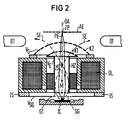
- the spectrometer objective shown schematically in FIGS. 1 and 2 essentially consists of a short focal length, largely asymmetrical objective lens OL, a single-stage deflection system DS arranged symmetrically to the optical axis OA within the magnetic lens OL and an electrostatic counterfield spectrometer which has an electrode arrangement SG, Gl for acceleration which has secondary electrons SE triggered on a sample IC, preferably in the integrated circuit, and an electrode pair K1 / K2 which generates a spherically symmetrical opposing field.
- the system consisting of objective lens OL, deflection unit OS and spectrometer forms the component of the electron-optical column of the one shown schematically in FIG.
- Electron beam measuring device with which the primary electrons PE emitted by a beam generator G are focused and deflected and the secondary electrons SE triggered on the sample IC are imaged in a point ZS lying on the optical axis OA.
- the electron source Q or its intermediate image ZP generated by condenser lenses KL is reduced with the aid of the spectrometer objective to the sample arranged in the immediate vicinity of the rear focal plane of the magnetic lens OL IC off.
- the positioning of the primary electron beam PE on a point of the sample IC, which is not described in more detail, or its line-shaped deflection is carried out with the aid of the deflection unit DS.
- the electrode arrangement for suctioning and accelerating the secondary electrons SE consists of a flat electrode SG arranged in the beam path directly above the sample IC and a grid electrode G1 arranged in the region of the lower pole piece of the objective lens OL, which preferably has a high positive potential V E of about 1 to 5 kV.
- the electrode SG which is insulated on the lower pole piece or within the pole piece gap, is supplied with a potential V SG lying between the sample potential (normally earth potential) and the potential V E of the electrode G1, in particular with a potential between 0 and 100 volts, that the field strength in the area of the sample IC remains below a critical value. In addition, it is ensured that unevenness of the sample surface has no influence on the homogeneity of the electrical field built up between the electrodes SG and G1.
- the lower electrode SG is preferably designed as a grid and has one by insulators IS lower pole piece of the objective lens OL separate annular holder part which is conductively connected to a variable voltage source. Instead of the grid electrode G1, a pinhole can of course also be used.
- the accelerated secondary electrons SE pass through the grid electrode G1 and reach the magnetic field of the objective lens OL between the pole pieces by focusing them in a point ZS lying on the optical axis OA.
- the position of this focusing point ZS which is to be interpreted as a real intermediate image of the virtual source below the sample IC (smallest caustic cross section of all virtual secondary electron tracks below the sample IC) of the secondary electrons SE, is determined by the height of the potential V E applied to the grid electrode G1 and the magnetic field strength in the pole shoe gap, which is dependent on the primary electron energy.
- the braking and the energy analysis of the secondary electrons SE takes place within or, as shown in FIGS. 1 and 2, above the objective lens OL in a spherically symmetrical electrical opposing field, that one lies in the space between two almost hemispherical, at different potentials V E and V G
- Grid electrodes K1 and K2 builds. While the lower grid electrode K1 is at the potential V E of the electrode G1, the upper grid electrode K2 is usually supplied with potentials between approximately -15 volts and +15 volts. Above the electrode arrangement K1 building up the opposing field, 1 and 2, the potential of which is preferably chosen to be equal to the potential V G of the electrode K2.
- the secondary electron focus ZS should be sufficiently far above the pole pieces and the deflection unit DS.
- the focusing of the secondary electrons in a point ZS of the optical axis OA above the deflection unit DS is possible the better, the smaller the energy of the primary electrons PE and the higher the potential V E of the electrode G1 chosen to accelerate the secondary electrons SE.
- the grid electrode K1 is conductively connected to the electrode G1 via a hollow cylinder HZ arranged concentrically to the optical axis OA.
- the spectrometer objective shown in Fig. 3 consists essentially of a short focal length objective lens OL, a deflection unit DS arranged symmetrically to the optical axis OA within the objective lens OL and an electrostatic counterfield spectrometer which the electrode arrangement SG / G1 known from FIGS. 1 and 2 for suction and Accelerate the secondary electrons SE and has an electrode arrangement K1 / K2 that generates a spherically symmetrical opposing field.
- the system consisting of objective lens OL, deflection unit DS and counter-field spectrometer forms the component of the electron-optical column of an electron beam measuring device with which the primary electrons PE emitted by a high-current electron source are focused and deflected and the secondary electrons SE triggered on the sample IC are preferably in the one on the optical axis OA Center ZS of the spherically symmetrical opposing field can be focused.
- This opposing field is generated with the aid of the grid electrodes K1 and K2 arranged in a housing GH above the objective lens OL, each of which has parts of the surface of concentric spheres with different radii R 1 and R 2 (R 1 ⁇ 30 mm, R 2 ⁇ 34 mm) form.
- the center point ZS defining the center of the opposing field of the balls assigned to the grid electrodes K1 and K2 lies very far above the deflection unit DS, which preferably consists of magnetic and electrical deflection elements MD or ED, and the pole shoe gap, lamella rotations of the secondary electrons SE become after the intermediate image ZS has passed through avoided.
- a hollow cylinder HZ consisting of three parts, arranged symmetrically to the optical axis OA.
- this hollow cylinder HZ which tapers in the region of the objective lens OL, is conductively connected to the electrode K1 lying at a potential V E
- the lower part thereof Partly terminated on the sample side by the electrode G1, which is also at the potential V E between approximately 0.5 and 5 kV, in particular 2 kV.
- the central cylinder part surrounded by the magnetic deflection element MD is in this case, as in the known spectrometer objective according to E.
- Plies designed as an electrostatic eight-pole deflector ED, the individual electrodes of which are subjected to a further potential V X for deflecting the primary beam.
- the stigmator ST to compensate for the axial astigmatism can be dispensed with if the electrodes of the eight-pole deflector ED are provided with suitable additional voltages.
- the homogeneous electric and magnetic fields generated with the aid of the deflection unit DS are spatially oriented to one another in the manner of a Wien filter in such a way that their field vectors are perpendicular to one another and in each case perpendicular to the speed vector of the secondary electrons SE.
- spectrometer lenses Due to the electrical delay field superimposed on the focusing magnetic field of the objective lens, spectrometer lenses have significantly smaller color and aperture error constants than magnetic single lenses. Since the imaging properties of such systems are essentially determined by the homogeneity and strength of the retardation field, the theoretically possible resolution limit (beam diameter on the sample) could not be reached due to the field distortion on the sample surface in conventional spectrometer objectives. The improved imaging properties only come with the decoupling of the delay field from the respective sample according to the invention of these electrostatic-magnetic lenses without restrictions.
- the invention is of course not limited to the exemplary embodiments shown in FIGS. 1 to 3. It is thus possible, for example, to arrange the electrode arrangement K1, K2 generating the spherically symmetrical opposing field and possibly also the detector system completely within the objective lens OL.
- This deflection system DS can of course also be arranged in a conventional manner in the corpuscular beam path above the objective lens OL.
- This deflection system DS can of course also be arranged in a conventional manner in the corpuscular beam path above the objective lens OL.
- the lengthening of the beam path also increases the disadvantageous influence of the Boersch effect on the probe diameter.
- a flat pair of electrodes can also be used to generate the opposing field.
- detection of the secondary electrons SE independent of the emission angle is no longer possible with such an arrangement.
Landscapes
- Chemical & Material Sciences (AREA)
- Analytical Chemistry (AREA)
- Analysing Materials By The Use Of Radiation (AREA)
- Electron Tubes For Measurement (AREA)
- Tests Of Electronic Circuits (AREA)
- Testing Or Measuring Of Semiconductors Or The Like (AREA)
- Other Investigation Or Analysis Of Materials By Electrical Means (AREA)
Claims (15)
- Objectif de spectromètre pour appareil de mesure à faisceau de corpuscules, comprenant une lentille d'objectif (OL) et un spectromètre à champ antagoniste qui forment un module opto-corpusculaire de focalisation d'un faisceau corpusculaire primaire (PE), le spectromètre à champ antagoniste comprenant une première disposition d'électrode (G1) pour l'accélération des corpuscules secondaires (SE) détachés d'un échantillon (IC) vers la lentille d'objectif (OL), ainsi qu'une seconde disposition d'électrodes (K1, K2) pour la création d'une barrière de potentiel (VG) freinant les corpuscules secondaires (SE) et une électrode (SG) disposée immédiatement au-dessus de l'échantillon (IC) et dont le potentiel est compris entre le potentiel de l'échantillon et le potentiel (VE) de la première disposition d'électrode (G1) est montée dans la marche du faisceau de corpuscules en amont de la première disposition d'électrode (G1), caractérisé en ce que l'électrode (SG) de réglage de l'intensité du champ au voisinage de l'échantillon est connectée à une source variable de tension.
- Objectif de spectromètre selon la revendication 1, caractérisé en ce que l'électrode (SG) est fixée à une pièce polaire inférieure de la lentille d'objectif (OL).
- Objectif de spectromètre selon l'une des revendications 1 et 2, caractérisé en ce que l'électrode (SG) est fixée dans un intervalle compris entre pièces polaires de la lentille de l'objectif (OL).
- Objectif de spectromètre selon l'une des revendications 1 à 3, caractérisé en ce que l'électrode (SG) comporte une pièce annulaire de fixation.
- Objectif de spectromètre selon l'une des revendications 1 à 4, caractérisé en ce que l'électrode (SG) est formée d'une grille.
- Objectif de spectromètre selon l'une des revendications 1 à 5, caractérisé en ce que l'électrode (SG) est formée d'un diaphragme.
- Objectif de spectromètre selon l'une des revendications 1 à 6, caractérisé en ce que la seconde disposition d'électrodes (K1, K2) est disposée au-dessus de la lentille d'objectif (OL).
- Objectif de spectromètre selon l'une des revendications 1 à 6 caractérisé en ce que la seconde disposition d'électrodes (K1, K2) est disposée à l'intérieur de la lentille d'objectif (OL).
- Objectif de spectromètre selon l'une des revendications 1 à 8, caractérisé en ce que la seconde disposition d'électrodes (K1, K2) comprend une première (K1) et une seconde (K2) électrode, en ce que la première électrode (K1) fait partie de la surface d'une première sphère ayant un premier rayon (R1), en ce que la seconde électrode (K2) fait partie de la surface d'une seconde sphère ayant un second rayon (R2), le centre des première et seconde sphères coïncidant en un point (ZS) situé sur l'axe optique (OA) de la lentille d'objectif (OL).
- Objectif de spectromètre selon l'une des revendications 1 à 9, caractérisé par un système de déviation (DS) intégré dans la lentille d'objectif (OL) et disposé au-dessus de la première disposition d'électrode (G1).
- Objectif de spectromètre selon l'une des revendications 1 à 10, caractérisé en ce que le système de déviation (DS, MD, ED) est conformé à la manière d'un filtre de Wien.
- Procédé d'examen d'échantillons, en particulier de circuits intégrés, qui utilise un objectif de spectromètre, suivant lequel- un faisceau corpusculaire primaire (PE) est focalisé par une lentille d'objectif (OL) sur un échantillon à examiner,- les corpuscules secondaires détachés de l'échantillon par un premier potentiel (VE) au moyen d'une première disposition d'électrode (G1) sont accélérés vers la lentille de l'objectif (OL),- les corpuscules secondaires détachés sont pompés sur l'échantillon par un potentiel (VSG) d'une électrode (SG) montée en amont de la première disposition d'électrode (G1), ce potentiel étant compris en un potentiel de l'échantillon et le premier potentiel (VE) et- les corpuscules secondaires sont ensuite freinés par une barrière de potentiel (VG) créée par une seconde disposition d'électrodes (K1, K2)caractérisé
en ce que le potentiel (VSG) de l'électrode montée en amont (SG) est réglable de manière variable pour le réglage de l'intensité du champ au voisinage de l'échantillon. - Procédé selon la revendication 12, caractérisé en ce que le second potentiel (VSG) est réglable entre 0 et 100 V.
- Procédé selon les revendications 12 ou 13, caractérisé en ce que la barrière de potentiel est formée par un champ antagoniste sphérique symétrique.
- Procédé selon l'une des revendications 12 à 14, caractérisé en ce que le faisceau de corpuscules primaires peut être dévié.
Applications Claiming Priority (2)
| Application Number | Priority Date | Filing Date | Title |
|---|---|---|---|
| DE19863638682 DE3638682A1 (de) | 1986-11-13 | 1986-11-13 | Spektrometerobjektiv fuer korpuskularstrahlmesstechnik |
| DE3638682 | 1986-11-13 |
Publications (3)
| Publication Number | Publication Date |
|---|---|
| EP0267555A2 EP0267555A2 (fr) | 1988-05-18 |
| EP0267555A3 EP0267555A3 (fr) | 1989-10-25 |
| EP0267555B1 true EP0267555B1 (fr) | 1997-02-12 |
Family
ID=6313810
Family Applications (1)
| Application Number | Title | Priority Date | Filing Date |
|---|---|---|---|
| EP87116416A Expired - Lifetime EP0267555B1 (fr) | 1986-11-13 | 1987-11-06 | Objectif de spectromètre pour appareils de mesure par faisceau corpusculaire et procédé pour l'examen d'échantillons. |
Country Status (4)
| Country | Link |
|---|---|
| US (1) | US4812651A (fr) |
| EP (1) | EP0267555B1 (fr) |
| JP (1) | JP2701034B2 (fr) |
| DE (2) | DE3638682A1 (fr) |
Families Citing this family (38)
| Publication number | Priority date | Publication date | Assignee | Title |
|---|---|---|---|---|
| JPS6452370A (en) * | 1987-08-24 | 1989-02-28 | Hitachi Ltd | Potential measuring apparatus |
| JP2765851B2 (ja) * | 1988-03-30 | 1998-06-18 | 株式会社日立製作所 | 電子検出器及びこれを用いた電子線装置 |
| US4943769A (en) * | 1989-03-21 | 1990-07-24 | International Business Machines Corporation | Apparatus and method for opens/shorts testing of capacitively coupled networks in substrates using electron beams |
| US4983830A (en) * | 1989-06-29 | 1991-01-08 | Seiko Instruments Inc. | Focused ion beam apparatus having charged particle energy filter |
| DE4027062A1 (de) * | 1990-08-27 | 1992-04-23 | Integrated Circuit Testing | Verfahren und anordnung zum testen und reparieren einer integrierten schaltung |
| JP3148353B2 (ja) * | 1991-05-30 | 2001-03-19 | ケーエルエー・インストルメンツ・コーポレーション | 電子ビーム検査方法とそのシステム |
| JP3730263B2 (ja) * | 1992-05-27 | 2005-12-21 | ケーエルエー・インストルメンツ・コーポレーション | 荷電粒子ビームを用いた自動基板検査の装置及び方法 |
| US5444243A (en) * | 1993-09-01 | 1995-08-22 | Hitachi, Ltd. | Wien filter apparatus with hyperbolic surfaces |
| JPH07161329A (ja) * | 1993-12-07 | 1995-06-23 | Fujitsu Ltd | 電子ビーム装置 |
| JP3291880B2 (ja) * | 1993-12-28 | 2002-06-17 | 株式会社日立製作所 | 走査形電子顕微鏡 |
| US5614833A (en) * | 1994-10-25 | 1997-03-25 | International Business Machines Corporation | Objective lens with large field deflection system and homogeneous large area secondary electron extraction field |
| JP3372138B2 (ja) * | 1995-06-26 | 2003-01-27 | 株式会社日立製作所 | 走査形電子顕微鏡 |
| DE69602936T2 (de) * | 1996-07-25 | 1999-11-04 | Act Advanced Circuit Testing Gesellschaft Fuer Testsystementwicklung Mbh | Detektor-Objektivlinse |
| GB9719417D0 (en) * | 1997-09-13 | 1997-11-12 | Univ York | Electron microscope |
| JP4215282B2 (ja) * | 1997-12-23 | 2009-01-28 | エフ イー アイ カンパニ | 静電対物レンズ及び電気走査装置を装備したsem |
| DE19845329C2 (de) * | 1998-03-10 | 2001-09-27 | Erik Essers | Rasterelektronenmikroskop |
| EP1068630B1 (fr) | 1998-03-10 | 2005-07-20 | Erik Essers | Microscope electronique a balayage |
| US6661008B2 (en) * | 1998-06-22 | 2003-12-09 | Nikon Corporation | Electron-optical system and inspection method using the same |
| EP1022766B1 (fr) * | 1998-11-30 | 2004-02-04 | Advantest Corporation | Appareil à faisceau de particules |
| DE69933921T2 (de) * | 1999-05-06 | 2007-03-01 | Advantest Corp. | Korpuskularstrahlgerät |
| EP1100112A1 (fr) * | 1999-11-12 | 2001-05-16 | Advantest Corporation | Objectif de spectromètre adapté pour un système de mesure de l'énergie d'un faisceau de particules |
| EP1139091B1 (fr) * | 2000-03-27 | 2009-08-19 | ELLCIE Maintenance GmbH | Spectromètre élétronique avec unité de déflection |
| DE60042758D1 (de) * | 2000-03-31 | 2009-09-24 | Hitachi Ltd | Abtast-elektronenmikroskop |
| US6847038B2 (en) * | 2002-07-15 | 2005-01-25 | Hitachi, Ltd. | Scanning electron microscope |
| US6407388B1 (en) * | 2000-04-18 | 2002-06-18 | Advantest Corp. | Corpuscular beam device |
| US20050026436A1 (en) * | 2000-12-21 | 2005-02-03 | Hogan Timothy J. | Method for improving ash rate uniformity in photoresist ashing process equipment |
| JP2004516631A (ja) * | 2000-12-22 | 2004-06-03 | フェイ カンパニ | 特に半導体ウェーハ用の粒子光学検査装置 |
| DE60118070T2 (de) * | 2001-09-04 | 2006-08-17 | Advantest Corp. | Partikelstrahlgerät |
| DE10301579A1 (de) * | 2003-01-16 | 2004-07-29 | Leo Elektronenmikroskopie Gmbh | Elektronenstrahlgerät und Detektoranordnung |
| DE10317894B9 (de) | 2003-04-17 | 2007-03-22 | Leo Elektronenmikroskopie Gmbh | Fokussiersystem für geladene Teilchen, Elektronenmikroskopiesystem und Elektronenmikroskopieverfahren |
| JP4519567B2 (ja) * | 2004-08-11 | 2010-08-04 | 株式会社日立ハイテクノロジーズ | 走査型電子顕微鏡およびこれを用いた試料観察方法 |
| DE602005010969D1 (de) * | 2005-03-17 | 2008-12-24 | Integrated Circuit Testing | Teilchenstrahlgerät für hohe räumliche Auflösung und verschiedene für perspektivische Abbildungsmethoden |
| GB0700754D0 (en) * | 2007-01-15 | 2007-02-21 | Oxford Instr Analytical Ltd | Charged particle analyser and method |
| US8759764B2 (en) * | 2012-06-29 | 2014-06-24 | Fei Company | On-axis detector for charged particle beam system |
| DE102013006535B4 (de) * | 2013-04-15 | 2025-11-06 | Carl Zeiss Microscopy Gmbh | Raster-Partikelstrahlmikroskop mit energiefilterndem Detektorsystem |
| DE102015210893B4 (de) | 2015-06-15 | 2019-05-09 | Carl Zeiss Microscopy Gmbh | Analyseeinrichtung zur Analyse der Energie geladener Teilchen und Teilchenstrahlgerät mit einer Analyseeinrichtung |
| DE112018007343B4 (de) | 2018-04-26 | 2023-11-23 | Hitachi High-Tech Corporation | Mit einem strahl geladener teilchen arbeitende vorrichtung |
| US10964522B2 (en) * | 2018-06-06 | 2021-03-30 | Kla Corporation | High resolution electron energy analyzer |
Family Cites Families (9)
| Publication number | Priority date | Publication date | Assignee | Title |
|---|---|---|---|---|
| GB1447983A (en) * | 1973-01-10 | 1976-09-02 | Nat Res Dev | Detector for electron microscopes |
| JPS5772073A (en) * | 1980-10-24 | 1982-05-06 | Fujitsu Ltd | Voltage measuring device |
| DE3138929A1 (de) * | 1981-09-30 | 1983-04-14 | Siemens AG, 1000 Berlin und 8000 München | Verbessertes sekundaerelektronen-spektrometer fuer die potentialmessung an einer probe mit einer elektronensonde |
| EP0113746B1 (fr) * | 1982-07-16 | 1988-01-07 | Lintech Instruments Limited | Systeme d'electrodes pour spectrometre a champ contrarie pour un appareil de mesure a faisceau electronique |
| GB8327737D0 (en) * | 1983-10-17 | 1983-11-16 | Texas Instruments Ltd | Electron detector |
| JPS60130044A (ja) * | 1983-12-16 | 1985-07-11 | Jeol Ltd | 走査電子顕微鏡 |
| EP0178431B1 (fr) * | 1984-09-18 | 1990-02-28 | ICT Integrated Circuit Testing Gesellschaft für HalbleiterprÀ¼ftechnik mbH | Spectromètre à champ inverse pour méthode de mesure à faisceau d'électrons |
| FR2575597B1 (fr) * | 1984-12-28 | 1987-03-20 | Onera (Off Nat Aerospatiale) | Appareil pour la micro-analyse ionique a tres haute resolution d'un echantillon solide |
| US4675524A (en) * | 1985-03-11 | 1987-06-23 | Siemens Aktiengesellschaft | Scanning particle microscope with diminished boersch effect |
-
1986
- 1986-11-13 DE DE19863638682 patent/DE3638682A1/de not_active Withdrawn
-
1987
- 1987-11-06 EP EP87116416A patent/EP0267555B1/fr not_active Expired - Lifetime
- 1987-11-06 DE DE3752020T patent/DE3752020D1/de not_active Expired - Lifetime
- 1987-11-11 JP JP62286409A patent/JP2701034B2/ja not_active Expired - Fee Related
- 1987-11-13 US US07/120,133 patent/US4812651A/en not_active Expired - Lifetime
Also Published As
| Publication number | Publication date |
|---|---|
| EP0267555A3 (fr) | 1989-10-25 |
| US4812651A (en) | 1989-03-14 |
| DE3752020D1 (de) | 1997-03-27 |
| JP2701034B2 (ja) | 1998-01-21 |
| EP0267555A2 (fr) | 1988-05-18 |
| JPS63146336A (ja) | 1988-06-18 |
| DE3638682A1 (de) | 1988-05-19 |
Similar Documents
| Publication | Publication Date | Title |
|---|---|---|
| EP0267555A2 (fr) | Objectif de spectromètre pour appareils de mesure par faisceau corpusculaire et procédé pour l'examen d'échantillons. | |
| EP0333018B1 (fr) | Lentille d'objectif pour la focalisation de particules chargées | |
| EP0281743B1 (fr) | Objectif détecteur pour microscope à balayage | |
| EP0461442B1 (fr) | Appareil à faisceau de particules | |
| EP0205184B1 (fr) | Objectif de faible aberration comportant un spectromètre de haute acceptance en électrons secondaires | |
| EP0274622B1 (fr) | Assemblage de détecteur avec un objectif muni d'un détecteur pour instruments à rayons corpusculaires | |
| EP0893816B1 (fr) | Appareil à faisceau corpusculaire | |
| EP0242602B1 (fr) | Lentille électrostatique et magnétique pour appareils à faisceau corpusculaire | |
| US4649316A (en) | Ion beam species filter and blanker | |
| EP0194570A2 (fr) | Microscope corpusculaire à balayage à effet Boersch réduit | |
| DE3532781A1 (de) | Anordnung zur detektion von sekundaer- und/oder rueckstreuelektronen in einem elektronenstrahlgeraet | |
| EP0205185B1 (fr) | Objectif comportant un spectromètre en technique de mesure par faisceau d'électrons | |
| JPH0286036A (ja) | イオンマイクロアナライザ | |
| EP0236807A2 (fr) | Objectif de spectromètre en technique de mesure par faisceau corpusculaire | |
| EP0348785A2 (fr) | Appareil de mesure par faisceau d'électrons | |
| DE102012215945A1 (de) | Teilchenstrahlgerät und Verfahren zum Betrieb eines Teilchenstrahlgeräts | |
| DE112018007343B4 (de) | Mit einem strahl geladener teilchen arbeitende vorrichtung | |
| DE602004012056T2 (de) | Fokussierlinse für Strahlen geladener Teilchen | |
| DE102015210893B4 (de) | Analyseeinrichtung zur Analyse der Energie geladener Teilchen und Teilchenstrahlgerät mit einer Analyseeinrichtung | |
| DE3703028A1 (de) | Rastermikroskop | |
| DE10235981A1 (de) | Teilchenoptische Vorrichtung und Elektronenmikroskop | |
| US5089699A (en) | Secondary charged particle analyzing apparatus and secondary charged particle extracting section | |
| DE102023131607A1 (de) | Verfahren zum Betreiben einer Teilchenstrahlvorrichtung, Computerprogrammprodukt und Teilchenstrahlvorrichtung zum Ausführen des Verfahrens | |
| DE4236273A1 (en) | Lens for focussing electrons for specimen inspection - has field generated by coils and cone-shaped electrode set into entry section | |
| EP1100112A1 (fr) | Objectif de spectromètre adapté pour un système de mesure de l'énergie d'un faisceau de particules |
Legal Events
| Date | Code | Title | Description |
|---|---|---|---|
| PUAI | Public reference made under article 153(3) epc to a published international application that has entered the european phase |
Free format text: ORIGINAL CODE: 0009012 |
|
| AK | Designated contracting states |
Kind code of ref document: A2 Designated state(s): DE FR GB IT NL |
|
| PUAL | Search report despatched |
Free format text: ORIGINAL CODE: 0009013 |
|
| AK | Designated contracting states |
Kind code of ref document: A3 Designated state(s): DE FR GB IT NL |
|
| 17P | Request for examination filed |
Effective date: 19891212 |
|
| RAP1 | Party data changed (applicant data changed or rights of an application transferred) |
Owner name: ICT INTEGRATED CIRCUIT TESTING GESELLSCHAFT FUER H |
|
| 17Q | First examination report despatched |
Effective date: 19920626 |
|
| RAP1 | Party data changed (applicant data changed or rights of an application transferred) |
Owner name: ICT INTEGRATED CIRCUIT TESTING GESELLSCHAFT FUER H Owner name: ADVANTEST CORPORATION |
|
| REG | Reference to a national code |
Ref country code: GB Ref legal event code: 732E |
|
| GRAG | Despatch of communication of intention to grant |
Free format text: ORIGINAL CODE: EPIDOS AGRA |
|
| GRAH | Despatch of communication of intention to grant a patent |
Free format text: ORIGINAL CODE: EPIDOS IGRA |
|
| RAP1 | Party data changed (applicant data changed or rights of an application transferred) |
Owner name: ADVANTEST CORPORATION Owner name: ACT ADVANCED CIRCUIT TESTING GESELLSCHAFT FUER TES |
|
| RTI1 | Title (correction) | ||
| RAP1 | Party data changed (applicant data changed or rights of an application transferred) |
Owner name: ADVANTEST CORPORATION |
|
| GRAH | Despatch of communication of intention to grant a patent |
Free format text: ORIGINAL CODE: EPIDOS IGRA |
|
| GRAA | (expected) grant |
Free format text: ORIGINAL CODE: 0009210 |
|
| ITF | It: translation for a ep patent filed | ||
| AK | Designated contracting states |
Kind code of ref document: B1 Designated state(s): DE FR GB IT NL |
|
| GBT | Gb: translation of ep patent filed (gb section 77(6)(a)/1977) |
Effective date: 19970224 |
|
| REF | Corresponds to: |
Ref document number: 3752020 Country of ref document: DE Date of ref document: 19970327 |
|
| ET | Fr: translation filed | ||
| PLBE | No opposition filed within time limit |
Free format text: ORIGINAL CODE: 0009261 |
|
| STAA | Information on the status of an ep patent application or granted ep patent |
Free format text: STATUS: NO OPPOSITION FILED WITHIN TIME LIMIT |
|
| 26N | No opposition filed | ||
| REG | Reference to a national code |
Ref country code: GB Ref legal event code: IF02 |
|
| PGFP | Annual fee paid to national office [announced via postgrant information from national office to epo] |
Ref country code: NL Payment date: 20061013 Year of fee payment: 20 |
|
| PGFP | Annual fee paid to national office [announced via postgrant information from national office to epo] |
Ref country code: GB Payment date: 20061016 Year of fee payment: 20 |
|
| PGFP | Annual fee paid to national office [announced via postgrant information from national office to epo] |
Ref country code: IT Payment date: 20061130 Year of fee payment: 20 |
|
| PGFP | Annual fee paid to national office [announced via postgrant information from national office to epo] |
Ref country code: DE Payment date: 20070126 Year of fee payment: 20 |
|
| REG | Reference to a national code |
Ref country code: GB Ref legal event code: PE20 |
|
| NLV7 | Nl: ceased due to reaching the maximum lifetime of a patent |
Effective date: 20071106 |
|
| PG25 | Lapsed in a contracting state [announced via postgrant information from national office to epo] |
Ref country code: NL Free format text: LAPSE BECAUSE OF EXPIRATION OF PROTECTION Effective date: 20071106 |
|
| PG25 | Lapsed in a contracting state [announced via postgrant information from national office to epo] |
Ref country code: GB Free format text: LAPSE BECAUSE OF EXPIRATION OF PROTECTION Effective date: 20071105 |
|
| PGFP | Annual fee paid to national office [announced via postgrant information from national office to epo] |
Ref country code: FR Payment date: 20061002 Year of fee payment: 20 |