EP0267708A1 - Dispositif de modulation de signaux optiques - Google Patents
Dispositif de modulation de signaux optiques Download PDFInfo
- Publication number
- EP0267708A1 EP0267708A1 EP87309373A EP87309373A EP0267708A1 EP 0267708 A1 EP0267708 A1 EP 0267708A1 EP 87309373 A EP87309373 A EP 87309373A EP 87309373 A EP87309373 A EP 87309373A EP 0267708 A1 EP0267708 A1 EP 0267708A1
- Authority
- EP
- European Patent Office
- Prior art keywords
- mode
- optical
- waveguides
- signals
- control function
- Prior art date
- Legal status (The legal status is an assumption and is not a legal conclusion. Google has not performed a legal analysis and makes no representation as to the accuracy of the status listed.)
- Granted
Links
Images

Classifications
-
- G—PHYSICS
- G02—OPTICS
- G02F—OPTICAL DEVICES OR ARRANGEMENTS FOR THE CONTROL OF LIGHT BY MODIFICATION OF THE OPTICAL PROPERTIES OF THE MEDIA OF THE ELEMENTS INVOLVED THEREIN; NON-LINEAR OPTICS; FREQUENCY-CHANGING OF LIGHT; OPTICAL LOGIC ELEMENTS; OPTICAL ANALOGUE/DIGITAL CONVERTERS
- G02F1/00—Devices or arrangements for the control of the intensity, colour, phase, polarisation or direction of light arriving from an independent light source, e.g. switching, gating or modulating; Non-linear optics
- G02F1/01—Devices or arrangements for the control of the intensity, colour, phase, polarisation or direction of light arriving from an independent light source, e.g. switching, gating or modulating; Non-linear optics for the control of the intensity, phase, polarisation or colour
- G02F1/21—Devices or arrangements for the control of the intensity, colour, phase, polarisation or direction of light arriving from an independent light source, e.g. switching, gating or modulating; Non-linear optics for the control of the intensity, phase, polarisation or colour by interference
- G02F1/225—Devices or arrangements for the control of the intensity, colour, phase, polarisation or direction of light arriving from an independent light source, e.g. switching, gating or modulating; Non-linear optics for the control of the intensity, phase, polarisation or colour by interference in an optical waveguide structure
Definitions
- the invention relates to an optical signal modulation device.
- Known optical signal modulation devices comprise first and second optical waveguides connected at one end to an optical signal splitting device which couples portions of an incoming optical signal into the waveguides and at the other end to an optical signal combining device which causes optical signals received from the waveguides to interfere; and first modulating means responsive to a first control signal to cause a relative phase shift between signals in the first and second optical waveguides, the first modulating means causing relative phase shifts in both TM mode and TE mode signals.
- Such devices are hereinafter referred to as of the kind described.
- Examples of known devices of the kind described are lithium niobate integrated optical Mach-Zehnder modulators.
- the effect of polarisation sensitivity is that the transfer characteristic of the device for TM and TE modes is significantly different. This leaves a particular problem when the device is used as an optical switch in which a two state control function such as a voltage can be determined which correctly switches one mode but which has little useful effect on the other mode. This is a particular problem when it is desired to turn off the switch.
- the non-coincidence of minima of the two transfer characteristics means that a proportion of one zero mode polarisation will continue to pass through the device when it is controlled in the off state.
- an optical signal modulation device of the kind described is characterised in that the device further comprises second modulating means responsive to a second control signal to cause a relative phase shift between signals of one mode in the first and second waveguides and to leave signals of the other mode substantially unaffected whereby the transfer characteristics of the two modes may be shifted relatively to one another in use in accordance with the second control function.
- a second modulating means is provided to cause a second relative phase shift between signals of one mode in the first and second waveguides.
- This property finds particular application for devices fabricated from lithium niobate, particularly Z cut lithium niobate since the electro-optic coefficients of lithium niobate which interact with the first modulating means have a nearly integral relationship (in fact related by a factor of 3).
- the two state control function applied to the first modulating means can be arranged to switch between potentials related by the same factor of 3 since this will have substantially the same effect on both the TM and TE optical modes.
- the second modulating means may act on the TM mode independently of the TE mode, preferably the second modulating means causes a relative phase shift between TE mode signals in the two waveguides.
- the first and second modulating means each comprise electric field generating means for generating respective electric fields which are substantially orthogonal to each other and to the waveguides.
- the electric field generated by the second modulating means extends across only one of the waveguides.
- the second modulating means will apply a substantially constant bias field.
- optical is intended to refer to that part of the electromagnetic spectrum which is generally known as the visible region together with those parts of the infra-red and ultra-violet regions at each end of the visible region which are capable of being transmitted by dielectric optical waveguides such as optical fibres.
- the output of the combining device is coupled with a single mode waveguide.
- This provides a simple way of causing the device to act as a switch since when the first control function takes up one state, only first or higher order mode signals will be generated at the combining device and will therefore not be guided by the single mode waveguide.
- the first control function takes up its other state, zero order modes will result which are guided by the single mode waveguide.
- Figure 1 illustrates a conventional Mach-Zehnder modulator which has been modified in a manner to be explained below.
- the modulator comprises first and second optical waveguides 1, 2 fabricated on Z cut lithium niobate by the standard Ti diffusion technique.
- An oxide buffer layer is employed in order to reduce the propagation loss for the TM optical mode.
- a pair of modulation electrodes 3, 4 are aligned directly above the optical waveguides 1, 2 thus ensuring that electro-optically induced phase shifts occur as a result of the interaction of the vertical component of the applied field and the r33(32.2 ⁇ 10 ⁇ 12mV ⁇ 1) or r13(10 ⁇ 10 ⁇ 12mV ⁇ 1) electro-optic coefficient of the substrate material for the TM and TE optical modes respectively.
- the modulator electronics are driven from a modulation voltage generator 21 to which a modulation potential is applied and where appropriate combined with a bias potential to generate the required control potential.
- the optical waveguides 1, 2 are coupled with respective arms 5, 6 of an optical beam splitter 7 having an input arm 8 along which incoming optical signals are fed.
- the output ends of the waveguides 1, 2 are coupled to respective input arms 9, 10 of a Y coupler 11 having an output arm 12 coupled with a single mode optical fibre 13.
- the device shown in Figure 1 differs from conventional devices by the inclusion of a second electrode pair 14, 15 aligned such that the gap between the electrodes 14, 15 overlies the waveguide 1 only.
- a horizontal electric field is generated between the electrodes 14, 15 the size of which is controlled by a bias potential generator 16 which generates a bias potential V2.
- This second electrode pair 14, 15 induces electro-optical phase shifts only in the TE optical mode passing along the waveguide 1 via the in teraction of the horizontal component of the applied electric field and the r22(6.8 ⁇ 10 ⁇ 10mV ⁇ 1) electro-optic coefficient.
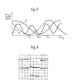
- the transfer characteristics of a conventional modulator device are indicated by the lines 17, 18 in Figure 2.
- the line 17 indicates the characteristic for the TM mode while the line 18 indicates the characteristic for the TE mode. It will be seen in Figure 2 that in general the maxima and minima of the characteristics do not occur at the same modulation potential V1. This is particularly undesirable where the device is used as a switch since it is desired to select two values for the modulation potential V1 which cause optical signals to be coupled into the single mode optical fibre 13 or not coupled respectively.
- an optical signal will be guided by the single mode fibre 13 if the portions of the signal fed along the waveguides 1, 2 are in phase on reaching the Y coupler 11 since this will produce a zero order mode at the Y coupler. There will be no guidance due to the formation of first and higher order modes at the Y coupler if there is a ⁇ phase shift between the signals at the Y coupler. These different phase shifts can be obtained by applying suitable potentials V1 to the modulator electodes 3, 4.
- a bias potential V2 is generated by the generator 16 and applied to the electrodes 14, 15.
- the bias potential generates an electric field between the electrodes 14, 15 which causes an additional phase shift on the TE mode signals in the optical waveguide 1 and the same signals in the waveguide 2.
- This causes the TE mode signals to interfere in a different manner at the Y coupler 11 and effectively shifts the transfer characteristic for the TE mode.
- the transfer characteristic can be shifted to take up a form similar to that indicated by the line 19 in Figure 2 in which a minimum of the TE mode characteristic 19 is coincident with a minimum of the TM mode characteristic 17. This occurs at a particular value of the modulation potential V1 indicated at V off in Figure 2.
- the device can be operated as a switch by causing the voltage V1 to take up one of the two values V off and V on .
- a switch control signal is supplied along a line 20 to the generator 5 which adds to the signal a suitable bias voltage to produce the desired value for V1.
- ⁇ is proportional to the electro-optic coefficient r nm being employed and thus the optical response of the device is dependent on the state of polarisation of the optical mode.
- the device described will still display a marked polarisation sensitivity for analogue modulation signals supplied along the line 20 but will produce quasi polarisation independent operation for digital modulation signals.
- Figure 3 shows the output for the two orthogonal modes when an electrical pulse of amplitude equal to three times the switching voltage for the TM mode is applied to the modulation electrodes.
- the optical output for the TM mode is driven to its maximum value but ringing appears on the leading and trailing edges due to the strong overdriving of the optical response. Since the ringing is totally confined to the leading and trailing edges of the optical pulse it is unlikely to introduce signficant system penalties at data rates where the rise and fall times of a binary 1 are far less than the bit time ie. ⁇ 1Gbit/s.
- the transition to the peak of the optical pulse occurs without ringing although additional insertion loss will arise since the peaks of the optical responses for the TE and TM modes do not exactly coincide since r33 and r13 are not precisely integrally related.
- the excess loss for the TE mode is estimated to be less than 0.1dB assuming the values of the electro-optic coefficients r13 r33 quoted earlier.
Landscapes
- Physics & Mathematics (AREA)
- Nonlinear Science (AREA)
- General Physics & Mathematics (AREA)
- Optics & Photonics (AREA)
- Optical Integrated Circuits (AREA)
- Optical Communication System (AREA)
- Optical Modulation, Optical Deflection, Nonlinear Optics, Optical Demodulation, Optical Logic Elements (AREA)
- Liquid Crystal (AREA)
Applications Claiming Priority (2)
| Application Number | Priority Date | Filing Date | Title |
|---|---|---|---|
| GB8625486 | 1986-10-24 | ||
| GB868625486A GB8625486D0 (en) | 1986-10-24 | 1986-10-24 | Optical signal modulation device |
Publications (2)
| Publication Number | Publication Date |
|---|---|
| EP0267708A1 true EP0267708A1 (fr) | 1988-05-18 |
| EP0267708B1 EP0267708B1 (fr) | 1994-09-14 |
Family
ID=10606243
Family Applications (1)
| Application Number | Title | Priority Date | Filing Date |
|---|---|---|---|
| EP87309373A Expired - Lifetime EP0267708B1 (fr) | 1986-10-24 | 1987-10-22 | Dispositif de modulation de signaux optiques |
Country Status (9)
| Country | Link |
|---|---|
| US (1) | US5004314A (fr) |
| EP (1) | EP0267708B1 (fr) |
| JP (1) | JP2737133B2 (fr) |
| AT (1) | ATE111613T1 (fr) |
| CA (1) | CA1290435C (fr) |
| DE (1) | DE3750539T2 (fr) |
| ES (1) | ES2058122T3 (fr) |
| GB (1) | GB8625486D0 (fr) |
| WO (1) | WO1988003278A1 (fr) |
Families Citing this family (21)
| Publication number | Priority date | Publication date | Assignee | Title |
|---|---|---|---|---|
| GB2211956B (en) * | 1987-11-05 | 1991-12-18 | Gen Electric Co Plc | Optical switch |
| DE59007534D1 (de) * | 1989-02-08 | 1994-12-01 | Reinhart Franz Karl | Integrierte optische Schaltung. |
| CA2011954C (fr) * | 1989-03-14 | 1994-02-22 | Fujitsu Limited | Modulateur optique |
| FR2658315A1 (fr) * | 1990-02-14 | 1991-08-16 | France Etat | Separateur de polarisations pour lumiere guidee. |
| FR2668615B1 (fr) * | 1990-10-31 | 1992-12-11 | France Etat | Separateur de polarisations pour lumiere guidee. |
| US5199086A (en) * | 1991-01-17 | 1993-03-30 | Massachusetts Institute Of Technology | Electro-optic system |
| JP2718854B2 (ja) * | 1992-06-10 | 1998-02-25 | 株式会社東芝 | 半導体装置 |
| US5323406A (en) * | 1992-11-02 | 1994-06-21 | Yee Ting K | Photonic mixer for photonically multiplying two electrical signals in two optically interconnected interferometric modulators operated at modulation outside the linear range |
| WO1994028455A1 (fr) * | 1993-06-01 | 1994-12-08 | United Technologies Corporation | Modulateur electro-optique dote d'un systeme de regulation de polarisation a activation par porte |
| DE19640725A1 (de) * | 1996-10-02 | 1998-04-09 | Reinhold Prof Dr Ing Noe | Netzwerkanalysator |
| US6204951B1 (en) | 1997-05-21 | 2001-03-20 | Keotrel Solutions, Inc. | Electro-optic modulator with improved harmonic performance |
| US6137619A (en) * | 1998-04-08 | 2000-10-24 | Nz Applied Technologies, Incorporated | High-speed electro-optic modulator |
| US6372284B1 (en) | 1998-06-11 | 2002-04-16 | Optelecom, Inc. | Fluoropolymer coating of lithium niobate integrated optical devices |
| US6479979B1 (en) * | 1999-07-09 | 2002-11-12 | Srico, Inc. | Opto-electric device for measuring the root-mean-square value of an alternating current voltage |
| US6404537B1 (en) | 2000-03-06 | 2002-06-11 | Corning Applied Technologies Corporation | Polarization transformer |
| US6522462B2 (en) | 2001-06-29 | 2003-02-18 | Super Light Wave Corp. | All optical logic using cross-phase modulation amplifiers and mach-zehnder interferometers with phase-shift devices |
| US20040165808A1 (en) * | 2003-02-20 | 2004-08-26 | Institut National D'optique | Optical repolarizing devices |
| JP4789460B2 (ja) * | 2004-12-22 | 2011-10-12 | 株式会社アドバンテスト | 光スイッチ及び光試験装置 |
| JP2008046573A (ja) * | 2006-08-21 | 2008-02-28 | Fujitsu Ltd | 光変調器 |
| US11070249B2 (en) * | 2017-09-28 | 2021-07-20 | British Telecommunications Public Limited Company | Controlling communications in respect of local area networks |
| CN111201718B (zh) | 2017-10-10 | 2021-10-01 | 英国电讯有限公司 | 识别局域网中的干扰链路 |
Citations (1)
| Publication number | Priority date | Publication date | Assignee | Title |
|---|---|---|---|---|
| US4291939A (en) * | 1978-03-24 | 1981-09-29 | The United States Of America As Represented By The Secretary Of The Navy | Polarization-independent optical switches/modulators |
Family Cites Families (2)
| Publication number | Priority date | Publication date | Assignee | Title |
|---|---|---|---|---|
| JPS561014A (en) * | 1979-06-18 | 1981-01-08 | Furukawa Electric Co Ltd:The | Optical filter of controllable transmission characteristic |
| JPS59228133A (ja) * | 1983-06-10 | 1984-12-21 | Yokogawa Hokushin Electric Corp | 分光装置 |
-
1986
- 1986-10-24 GB GB868625486A patent/GB8625486D0/en active Pending
-
1987
- 1987-10-20 WO PCT/GB1987/000738 patent/WO1988003278A1/fr not_active Ceased
- 1987-10-20 JP JP62506659A patent/JP2737133B2/ja not_active Expired - Fee Related
- 1987-10-20 US US07/209,622 patent/US5004314A/en not_active Expired - Lifetime
- 1987-10-22 EP EP87309373A patent/EP0267708B1/fr not_active Expired - Lifetime
- 1987-10-22 ES ES87309373T patent/ES2058122T3/es not_active Expired - Lifetime
- 1987-10-22 DE DE3750539T patent/DE3750539T2/de not_active Expired - Fee Related
- 1987-10-22 AT AT87309373T patent/ATE111613T1/de not_active IP Right Cessation
- 1987-10-23 CA CA000550140A patent/CA1290435C/fr not_active Expired - Lifetime
Patent Citations (1)
| Publication number | Priority date | Publication date | Assignee | Title |
|---|---|---|---|---|
| US4291939A (en) * | 1978-03-24 | 1981-09-29 | The United States Of America As Represented By The Secretary Of The Navy | Polarization-independent optical switches/modulators |
Non-Patent Citations (2)
| Title |
|---|
| IEEE JOURNAL OF QUANTUM ELECTRONICS, vol. QE-17, no. 6, June 1981, pages 946-959, IEEE, New York, US; R.C. ALFERNESS: "Guided-wave devices for optical communication" * |
| OPTICS LETTERS, vol. 5, no. 5, May 1980, pages 176-178, Optical Society of America; C.H. BULMER et al.: "Linear interferometric waveguide modulator for electromagnetic-field detection" * |
Also Published As
| Publication number | Publication date |
|---|---|
| JP2737133B2 (ja) | 1998-04-08 |
| JPH01501575A (ja) | 1989-06-01 |
| DE3750539D1 (de) | 1994-10-20 |
| ATE111613T1 (de) | 1994-09-15 |
| GB8625486D0 (en) | 1986-11-26 |
| US5004314A (en) | 1991-04-02 |
| DE3750539T2 (de) | 1995-03-09 |
| CA1290435C (fr) | 1991-10-08 |
| WO1988003278A1 (fr) | 1988-05-05 |
| ES2058122T3 (es) | 1994-11-01 |
| EP0267708B1 (fr) | 1994-09-14 |
Similar Documents
| Publication | Publication Date | Title |
|---|---|---|
| EP0267708B1 (fr) | Dispositif de modulation de signaux optiques | |
| JP3929814B2 (ja) | マッハ−ツェンダ電子−光学変調器 | |
| US5991471A (en) | Configurable chirp mach-zehnder optical modulator | |
| KR0162755B1 (ko) | 고분자 도파로형 광 세기 변조기 | |
| EP0484791B1 (fr) | Procédé et dispositif pour modulation externe d'une porteuse optique | |
| US4709978A (en) | Mach-Zehnder integrated optical modulator | |
| CA2114662C (fr) | Modulateur electro-optique a inversion de domaines periodique | |
| US5408544A (en) | Optical modulator for producing a controllable chirp | |
| EP0817988B1 (fr) | Modulateur electro-optique non affecte par la polarisation | |
| EP2545408B1 (fr) | Modulateurs optiques à compression d'impulsions réglable | |
| EP0674210B1 (fr) | Modulateur optique | |
| US5285507A (en) | Controllable polarisation transformer | |
| US5185830A (en) | Optical waveguide directional coupler including control electrodes | |
| US4871223A (en) | Arrangement comprising at least one integrated optical waveguide on a substrate of electro-optical material and comprising at least one electrode | |
| US5917642A (en) | Optical modulator | |
| EP0827598A2 (fr) | Modulateurs optiques integres | |
| EP1217425B1 (fr) | Modulateur d'intensité optique et méthode correspondante | |
| Booth | LiNbO3 integrated optic devices for coherent optical fibre systems | |
| US20020105713A1 (en) | Fiber modulator and associated method | |
| JP2664749B2 (ja) | 光変調装置 | |
| RU1804672C (ru) | Управл емый волоконно-оптический СВЧ-фазовращатель | |
| JPH09218384A (ja) | 光制御素子及びその使用方法 | |
| Madabhushi | Lithium niobate optical modulators | |
| WO2002084385A2 (fr) | Optimisation de guide d'onde destine a un modulateur electro-optique de polymere polarise de sensibilite maximum | |
| KR19980035328A (ko) | 편광독립 전기광학 광 위상변조기 및 그를 이용한 광 스위치와 광 강도 변조기 |
Legal Events
| Date | Code | Title | Description |
|---|---|---|---|
| PUAI | Public reference made under article 153(3) epc to a published international application that has entered the european phase |
Free format text: ORIGINAL CODE: 0009012 |
|
| AK | Designated contracting states |
Kind code of ref document: A1 Designated state(s): AT BE CH DE ES FR GB GR IT LI LU NL SE |
|
| 17P | Request for examination filed |
Effective date: 19881017 |
|
| RAP3 | Party data changed (applicant data changed or rights of an application transferred) |
Owner name: BRITISH TELECOMMUNICATIONS PUBLIC LIMITED COMPANY |
|
| 17Q | First examination report despatched |
Effective date: 19910103 |
|
| GRAA | (expected) grant |
Free format text: ORIGINAL CODE: 0009210 |
|
| AK | Designated contracting states |
Kind code of ref document: B1 Designated state(s): AT BE CH DE ES FR GB GR IT LI LU NL SE |
|
| PG25 | Lapsed in a contracting state [announced via postgrant information from national office to epo] |
Ref country code: LI Effective date: 19940914 Ref country code: GR Free format text: LAPSE BECAUSE OF FAILURE TO SUBMIT A TRANSLATION OF THE DESCRIPTION OR TO PAY THE FEE WITHIN THE PRESCRIBED TIME-LIMIT Effective date: 19940914 Ref country code: CH Effective date: 19940914 Ref country code: BE Effective date: 19940914 Ref country code: AT Effective date: 19940914 |
|
| REF | Corresponds to: |
Ref document number: 111613 Country of ref document: AT Date of ref document: 19940915 Kind code of ref document: T |
|
| ITF | It: translation for a ep patent filed | ||
| REF | Corresponds to: |
Ref document number: 3750539 Country of ref document: DE Date of ref document: 19941020 |
|
| PG25 | Lapsed in a contracting state [announced via postgrant information from national office to epo] |
Ref country code: LU Free format text: LAPSE BECAUSE OF NON-PAYMENT OF DUE FEES Effective date: 19941031 |
|
| REG | Reference to a national code |
Ref country code: ES Ref legal event code: FG2A Ref document number: 2058122 Country of ref document: ES Kind code of ref document: T3 |
|
| REG | Reference to a national code |
Ref country code: CH Ref legal event code: PL |
|
| EAL | Se: european patent in force in sweden |
Ref document number: 87309373.6 |
|
| ET | Fr: translation filed | ||
| PLBE | No opposition filed within time limit |
Free format text: ORIGINAL CODE: 0009261 |
|
| STAA | Information on the status of an ep patent application or granted ep patent |
Free format text: STATUS: NO OPPOSITION FILED WITHIN TIME LIMIT |
|
| 26N | No opposition filed | ||
| PGFP | Annual fee paid to national office [announced via postgrant information from national office to epo] |
Ref country code: SE Payment date: 19970918 Year of fee payment: 11 |
|
| PGFP | Annual fee paid to national office [announced via postgrant information from national office to epo] |
Ref country code: ES Payment date: 19971008 Year of fee payment: 11 |
|
| PG25 | Lapsed in a contracting state [announced via postgrant information from national office to epo] |
Ref country code: SE Free format text: LAPSE BECAUSE OF NON-PAYMENT OF DUE FEES Effective date: 19981023 Ref country code: ES Free format text: LAPSE BECAUSE OF THE APPLICANT RENOUNCES Effective date: 19981023 |
|
| EUG | Se: european patent has lapsed |
Ref document number: 87309373.6 |
|
| PGFP | Annual fee paid to national office [announced via postgrant information from national office to epo] |
Ref country code: NL Payment date: 20000425 Year of fee payment: 13 |
|
| REG | Reference to a national code |
Ref country code: GB Ref legal event code: 732E |
|
| REG | Reference to a national code |
Ref country code: ES Ref legal event code: FD2A Effective date: 20001009 |
|
| PG25 | Lapsed in a contracting state [announced via postgrant information from national office to epo] |
Ref country code: NL Free format text: LAPSE BECAUSE OF NON-PAYMENT OF DUE FEES Effective date: 20010501 |
|
| NLV4 | Nl: lapsed or anulled due to non-payment of the annual fee |
Effective date: 20010501 |
|
| REG | Reference to a national code |
Ref country code: GB Ref legal event code: IF02 |
|
| PGFP | Annual fee paid to national office [announced via postgrant information from national office to epo] |
Ref country code: FR Payment date: 20020906 Year of fee payment: 16 |
|
| PGFP | Annual fee paid to national office [announced via postgrant information from national office to epo] |
Ref country code: GB Payment date: 20020916 Year of fee payment: 16 |
|
| PGFP | Annual fee paid to national office [announced via postgrant information from national office to epo] |
Ref country code: DE Payment date: 20020924 Year of fee payment: 16 |
|
| PG25 | Lapsed in a contracting state [announced via postgrant information from national office to epo] |
Ref country code: GB Free format text: LAPSE BECAUSE OF NON-PAYMENT OF DUE FEES Effective date: 20031022 |
|
| PG25 | Lapsed in a contracting state [announced via postgrant information from national office to epo] |
Ref country code: DE Free format text: LAPSE BECAUSE OF NON-PAYMENT OF DUE FEES Effective date: 20040501 |
|
| GBPC | Gb: european patent ceased through non-payment of renewal fee |
Effective date: 20031022 |
|
| PG25 | Lapsed in a contracting state [announced via postgrant information from national office to epo] |
Ref country code: FR Free format text: LAPSE BECAUSE OF NON-PAYMENT OF DUE FEES Effective date: 20040630 |
|
| REG | Reference to a national code |
Ref country code: FR Ref legal event code: ST |
|
| PG25 | Lapsed in a contracting state [announced via postgrant information from national office to epo] |
Ref country code: IT Free format text: LAPSE BECAUSE OF NON-PAYMENT OF DUE FEES;WARNING: LAPSES OF ITALIAN PATENTS WITH EFFECTIVE DATE BEFORE 2007 MAY HAVE OCCURRED AT ANY TIME BEFORE 2007. THE CORRECT EFFECTIVE DATE MAY BE DIFFERENT FROM THE ONE RECORDED. Effective date: 20051022 |