EP0269510A2 - Structure pour un dispositif à effet Hall - Google Patents
Structure pour un dispositif à effet Hall Download PDFInfo
- Publication number
- EP0269510A2 EP0269510A2 EP87402585A EP87402585A EP0269510A2 EP 0269510 A2 EP0269510 A2 EP 0269510A2 EP 87402585 A EP87402585 A EP 87402585A EP 87402585 A EP87402585 A EP 87402585A EP 0269510 A2 EP0269510 A2 EP 0269510A2
- Authority
- EP
- European Patent Office
- Prior art keywords
- output electrodes
- electrodes
- pair
- hall
- main body
- Prior art date
- Legal status (The legal status is an assumption and is not a legal conclusion. Google has not performed a legal analysis and makes no representation as to the accuracy of the status listed.)
- Withdrawn
Links
- 230000005284 excitation Effects 0.000 claims abstract description 27
- 239000000463 material Substances 0.000 claims abstract description 19
- 230000005355 Hall effect Effects 0.000 claims abstract description 12
- 230000001747 exhibiting effect Effects 0.000 claims abstract description 6
- 238000004519 manufacturing process Methods 0.000 description 5
- 230000005611 electricity Effects 0.000 description 4
- JBRZTFJDHDCESZ-UHFFFAOYSA-N AsGa Chemical compound [As]#[Ga] JBRZTFJDHDCESZ-UHFFFAOYSA-N 0.000 description 3
- 230000000694 effects Effects 0.000 description 3
- 230000008030 elimination Effects 0.000 description 3
- 238000003379 elimination reaction Methods 0.000 description 3
- 238000005259 measurement Methods 0.000 description 3
- 239000010409 thin film Substances 0.000 description 3
- RPQDHPTXJYYUPQ-UHFFFAOYSA-N indium arsenide Chemical compound [In]#[As] RPQDHPTXJYYUPQ-UHFFFAOYSA-N 0.000 description 2
- 239000007787 solid Substances 0.000 description 2
- 238000009966 trimming Methods 0.000 description 2
- QNRATNLHPGXHMA-XZHTYLCXSA-N (r)-(6-ethoxyquinolin-4-yl)-[(2s,4s,5r)-5-ethyl-1-azabicyclo[2.2.2]octan-2-yl]methanol;hydrochloride Chemical compound Cl.C([C@H]([C@H](C1)CC)C2)CN1[C@@H]2[C@H](O)C1=CC=NC2=CC=C(OCC)C=C21 QNRATNLHPGXHMA-XZHTYLCXSA-N 0.000 description 1
- 229910001218 Gallium arsenide Inorganic materials 0.000 description 1
- 238000013459 approach Methods 0.000 description 1
- 239000003795 chemical substances by application Substances 0.000 description 1
- 230000008878 coupling Effects 0.000 description 1
- 238000010168 coupling process Methods 0.000 description 1
- 238000005859 coupling reaction Methods 0.000 description 1
- 230000001419 dependent effect Effects 0.000 description 1
- 238000006073 displacement reaction Methods 0.000 description 1
- 230000005684 electric field Effects 0.000 description 1
- 230000007613 environmental effect Effects 0.000 description 1
- WPYVAWXEWQSOGY-UHFFFAOYSA-N indium antimonide Chemical compound [Sb]#[In] WPYVAWXEWQSOGY-UHFFFAOYSA-N 0.000 description 1
- 238000012886 linear function Methods 0.000 description 1
- 238000000034 method Methods 0.000 description 1
- 238000012986 modification Methods 0.000 description 1
- 230000004048 modification Effects 0.000 description 1
- 230000009467 reduction Effects 0.000 description 1
- 230000035945 sensitivity Effects 0.000 description 1
- 238000006467 substitution reaction Methods 0.000 description 1
- 239000000758 substrate Substances 0.000 description 1
- 230000005641 tunneling Effects 0.000 description 1
Images
Classifications
-
- H—ELECTRICITY
- H10—SEMICONDUCTOR DEVICES; ELECTRIC SOLID-STATE DEVICES NOT OTHERWISE PROVIDED FOR
- H10N—ELECTRIC SOLID-STATE DEVICES NOT OTHERWISE PROVIDED FOR
- H10N52/00—Hall-effect devices
Definitions
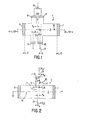
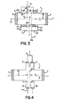
- the invention concerns Hall devices and, more particularly, an improved structure for a Hall device whereby first and second order voltage offsets can be eliminated or readily compensated.
Landscapes
- Hall/Mr Elements (AREA)
- Measuring Magnetic Variables (AREA)
Applications Claiming Priority (2)
| Application Number | Priority Date | Filing Date | Title |
|---|---|---|---|
| US06/933,444 US4698522A (en) | 1986-11-21 | 1986-11-21 | Structure for Hall device for compensation of first and second order voltage offsets |
| US933444 | 1992-08-21 |
Publications (2)
| Publication Number | Publication Date |
|---|---|
| EP0269510A2 true EP0269510A2 (fr) | 1988-06-01 |
| EP0269510A3 EP0269510A3 (fr) | 1989-05-24 |
Family
ID=25463976
Family Applications (1)
| Application Number | Title | Priority Date | Filing Date |
|---|---|---|---|
| EP87402585A Withdrawn EP0269510A3 (fr) | 1986-11-21 | 1987-11-17 | Structure pour un dispositif à effet Hall |
Country Status (4)
| Country | Link |
|---|---|
| US (1) | US4698522A (fr) |
| EP (1) | EP0269510A3 (fr) |
| BR (1) | BR8706288A (fr) |
| CA (1) | CA1283170C (fr) |
Cited By (1)
| Publication number | Priority date | Publication date | Assignee | Title |
|---|---|---|---|---|
| DE19954360A1 (de) * | 1999-11-11 | 2001-05-23 | Fraunhofer Ges Forschung | Hall-Element |
Families Citing this family (6)
| Publication number | Priority date | Publication date | Assignee | Title |
|---|---|---|---|---|
| US5543988A (en) * | 1993-04-30 | 1996-08-06 | International Business Machines Corporation | Hall sensor with high spatial resolution in two directions concurrently |
| DE4336482A1 (de) * | 1993-10-26 | 1995-04-27 | Bosch Gmbh Robert | Verfahren zum Abgleichen eines magnetoresistiven Sensors |
| JP3081751B2 (ja) * | 1994-03-03 | 2000-08-28 | 株式会社東芝 | 電気量測定装置 |
| DE10228805B4 (de) * | 2002-06-27 | 2008-11-13 | Infineon Technologies Ag | Hallsensorelement |
| US20040164840A1 (en) * | 2003-02-21 | 2004-08-26 | Brown University Research Foundation | Extraordinary hall effect sensors and arrays |
| US10679909B2 (en) * | 2016-11-21 | 2020-06-09 | Kla-Tencor Corporation | System, method and non-transitory computer readable medium for tuning sensitivies of, and determining a process window for, a modulated wafer |
Family Cites Families (5)
| Publication number | Priority date | Publication date | Assignee | Title |
|---|---|---|---|---|
| US3348184A (en) * | 1967-10-17 | Hall generator | ||
| JPS5249785A (en) * | 1975-10-20 | 1977-04-21 | Hitachi Ltd | Hall effect element |
| JPS5574661A (en) * | 1978-12-01 | 1980-06-05 | Toshiba Corp | Unbalanced voltage compensation circuit for hall element |
| JPS57107087A (en) * | 1980-12-25 | 1982-07-03 | Toshiba Corp | Hall effect device |
| JPS57177583A (en) * | 1981-04-14 | 1982-11-01 | Int Standard Electric Corp | Holl effect device |
-
1986
- 1986-11-21 US US06/933,444 patent/US4698522A/en not_active Expired - Lifetime
-
1987
- 1987-11-17 EP EP87402585A patent/EP0269510A3/fr not_active Withdrawn
- 1987-11-20 BR BR8706288A patent/BR8706288A/pt unknown
- 1987-11-20 CA CA000552304A patent/CA1283170C/fr not_active Expired - Lifetime
Non-Patent Citations (3)
| Title |
|---|
| IBM TECHNICAL DISCLOSURE BULLETIN, vol. 26, no. 10A, March 1984, pages 5065-5068, New York, US; M.H. BRODSKY et al.: "Quantized Hall effect circuit technology" * |
| PHYSICAL REVIEW B. CONDENSED MATTER, vol. 32, no. 10, November 1985, pages 6620-6629, The American Physical Society, Ridge, New York, US; D.A. SYPHERS et al.: "Contiguous two-dimensional regions in the quantized Hall regime" * |
| PHYSICAL REVIEW B. CONDENSED MATTER, vol. 35, no. 5, 15th February 1987, pages 2188-2197, The American Physical Society, New York, US; Q. NIU et al.: "Quantum Hall effect with realistic boundary conditions" * |
Cited By (3)
| Publication number | Priority date | Publication date | Assignee | Title |
|---|---|---|---|---|
| DE19954360A1 (de) * | 1999-11-11 | 2001-05-23 | Fraunhofer Ges Forschung | Hall-Element |
| DE19954360C2 (de) * | 1999-11-11 | 2001-09-20 | Fraunhofer Ges Forschung | Hall-Element |
| US6727563B1 (en) | 1999-11-11 | 2004-04-27 | Fraunhofer-Gesellschaft zur Fürderung der angewandten Forschung e.V. | Offset-reduced hall element |
Also Published As
| Publication number | Publication date |
|---|---|
| BR8706288A (pt) | 1988-06-28 |
| CA1283170C (fr) | 1991-04-16 |
| EP0269510A3 (fr) | 1989-05-24 |
| US4698522A (en) | 1987-10-06 |
Similar Documents
| Publication | Publication Date | Title |
|---|---|---|
| US4823075A (en) | Current sensor using hall-effect device with feedback | |
| US4361805A (en) | Magnetoresistive displacement sensor arrangement | |
| US5521501A (en) | Magnetic field sensor constructed from a remagnetization line and one magnetoresistive resistor or a plurality of magnetoresistive resistors | |
| Koon | Effect of contact size and placement, and of resistive inhomogeneities on van der Pauw measurements | |
| US20120262164A1 (en) | Magneto-resistive sensor for measuring magnetic fields | |
| Munter | A low-offset spinning-current Hall plate | |
| EP0151002B1 (fr) | Détecteur magnétique | |
| US5686879A (en) | Ammeter | |
| US6191581B1 (en) | Planar thin-film magnetic field sensor for determining directional magnetic fields | |
| Taylor et al. | On the use of the ac Josephson effect to maintain standards of electromotive force | |
| EP0859964A2 (fr) | Procede de reduction de la tension de decalage d'un dispositif hall | |
| US4200814A (en) | Multiplier with hall element | |
| US4698522A (en) | Structure for Hall device for compensation of first and second order voltage offsets | |
| EP0217478B1 (fr) | Transducteur d'angle sans contact | |
| JPH07190804A (ja) | 磁気抵抗式センサ装置を備えた磁界測定装置 | |
| US5646527A (en) | Hall-effect device with current and hall-voltage connections | |
| Boerger et al. | Generalized Hall‐effect measurement geometries and limitations of van der Pauw‐type Hall‐effect measurements | |
| US4683535A (en) | Thin film magnetometer | |
| US6784012B2 (en) | Method for measuring temperature in a wide range using a tunnel junction | |
| JPS63212803A (ja) | 変位計測装置 | |
| Berkes | Hall generators | |
| He et al. | Exceptionally accurate large graphene quantum Hall arrays for the new SI | |
| JP2663460B2 (ja) | 磁気方位センサ | |
| JP3492825B2 (ja) | 磁気抵抗型変位センサ | |
| JP2923959B2 (ja) | 磁気方位検出装置 |
Legal Events
| Date | Code | Title | Description |
|---|---|---|---|
| PUAI | Public reference made under article 153(3) epc to a published international application that has entered the european phase |
Free format text: ORIGINAL CODE: 0009012 |
|
| AK | Designated contracting states |
Kind code of ref document: A2 Designated state(s): AT BE CH DE ES FR GB GR IT LI LU NL SE |
|
| PUAL | Search report despatched |
Free format text: ORIGINAL CODE: 0009013 |
|
| AK | Designated contracting states |
Kind code of ref document: A3 Designated state(s): AT BE CH DE ES FR GB GR IT LI LU NL SE |
|
| 17P | Request for examination filed |
Effective date: 19891026 |
|
| 17Q | First examination report despatched |
Effective date: 19920326 |
|
| RAP1 | Party data changed (applicant data changed or rights of an application transferred) |
Owner name: SCHLUMBERGER INDUSTRIES, INC. |
|
| STAA | Information on the status of an ep patent application or granted ep patent |
Free format text: STATUS: THE APPLICATION IS DEEMED TO BE WITHDRAWN |
|
| 18D | Application deemed to be withdrawn |
Effective date: 19940125 |
|
| RIN1 | Information on inventor provided before grant (corrected) |
Inventor name: CAMPBELL, DANIEL P. Inventor name: LARSON, JAMES W. |