EP0269845A1 - Endverstärker für Reizstromgerät - Google Patents
Endverstärker für Reizstromgerät Download PDFInfo
- Publication number
- EP0269845A1 EP0269845A1 EP87115679A EP87115679A EP0269845A1 EP 0269845 A1 EP0269845 A1 EP 0269845A1 EP 87115679 A EP87115679 A EP 87115679A EP 87115679 A EP87115679 A EP 87115679A EP 0269845 A1 EP0269845 A1 EP 0269845A1
- Authority
- EP
- European Patent Office
- Prior art keywords
- power
- stage
- transistor circuit
- current
- circuit
- Prior art date
- Legal status (The legal status is an assumption and is not a legal conclusion. Google has not performed a legal analysis and makes no representation as to the accuracy of the status listed.)
- Granted
Links
- 238000011144 upstream manufacturing Methods 0.000 claims abstract description 4
- 230000000638 stimulation Effects 0.000 claims description 4
- 230000003321 amplification Effects 0.000 abstract 1
- 238000003199 nucleic acid amplification method Methods 0.000 abstract 1
- 239000003990 capacitor Substances 0.000 description 4
- 230000006378 damage Effects 0.000 description 1
- 230000003247 decreasing effect Effects 0.000 description 1
- 238000010586 diagram Methods 0.000 description 1
- 230000010355 oscillation Effects 0.000 description 1
- 230000000717 retained effect Effects 0.000 description 1
Images
Classifications
-
- H—ELECTRICITY
- H03—ELECTRONIC CIRCUITRY
- H03K—PULSE TECHNIQUE
- H03K5/00—Manipulating of pulses not covered by one of the other main groups of this subclass
- H03K5/01—Shaping pulses
- H03K5/02—Shaping pulses by amplifying
Definitions
- the invention relates to a power amplifier for an electrical stimulation device according to the features of the preamble of claim 1.
- Power amplifiers of this type usually comprise a driver stage with a downstream power stage.
- CC constant current mode
- an input-side control differential amplifier is used, the input of which is coupled against the output of the power stage via a resistor arrangement. If the current changes at the output of the power stage, the change is thus fed back to the control differential amplifier, which then regulates it out.
- the object of the present invention is to provide means in a power amplifier of the type mentioned at the outset which permit constant-voltage operation without the risk of oscillation generation or transistor destruction.
- the current limiter circuit between the driver stage and the power stage ensures that the voltage at the output of the current source transistor circuit does not also go to zero even in the event of a short circuit at the output of the power stage, but is retained as a possible control voltage. In constant voltage operation, there is still sufficient control voltage so that short-circuit regulation with all the negative consequences described above is avoided.
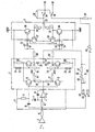
- the figure shows a circuit diagram of the power amplifier according to the invention.
- the power amplifier (push-pull amplifier) comprises a power stage 1, an upstream driver stage 2 and an input-side control differential amplifier 3.
- the component 4 is a preamplifier.
- the control differential amplifier comprises an operational amplifier 5, which is connected to an ohmic resistor 6 and capacitors 7, 8.
- the components 9, 9 ⁇ and 10 are ohmic resistors or a capacitor.
- the driver stage 2 contains control transformer transistors 11, 12 and current source transistors 13, 14, which are connected in push-pull mode (for bipolar operation of the stimulation current device).
- the components 15 to 20 are ohmic resistors and the components 21 to 26 are diodes.
- Power stage 1 also includes current limiting transistors 27, 28 and power transistors 29, 30 connected in push-pull mode.
- Components 31, 32 are current measuring resistors at output 33 of power stage 1.
- the output 33 of the power stage 1 can be connected to the one electrode connection socket 35 via a relay contact 34.
- the second electrode connection socket 36 is connected to ground on the one hand via a low-resistance (e.g. 22 ohm) current measuring resistor 37 and, on the other hand, can be short-circuited to the electrode connection socket 35 via a further relay contact 38 when the inner circuit of the stimulation current device is switched off (broken position of the contact 34).
- Element 39 is an ohmic test resistor.
- the current measuring resistor 37 is connected via a potentiometer 40 to the switch contact 41 for constant current operation (CC) of a changeover switch 42.
- the changeover switch 42 is in the position shown on the switch contact 43.
- the output 44 of the driver stage 2 between the two diodes 25, 26 is connected to the input of the control differential amplifier 3 via a gain setting element 45.
- the gain setting element 45 comprises a potentiometer 46, an ohmic fixed resistor 47 and a capacitor 48.
- the collectors of the current source transistors 13, 14 are also in the driver stage 2 via ohmic current limiting resistors 49, 50 (for example 1 k ⁇ ) and diodes 51, 52 with capacitors 53, 54 connected in parallel with the collectors of the current limiting transistors 27, 28 and the bases of the power transistors 29, 30 connected.
- the current limiting resistors 49, 50 ensure a voltage drop in the event of a short circuit at the output power level 1.
- the voltage at output 44 of the driver level never drops to zero. There is always a sufficient amount of residual voltage that can be fed back as a control voltage in the sense of the invention.
- the diodes 51, 52 prevent countercurrent operation of the transistors 27, 28, 29, 30 of the power stage 1 in the worst case.
Landscapes
- Physics & Mathematics (AREA)
- Nonlinear Science (AREA)
- Amplifiers (AREA)
Abstract
Description
- Die Erfindung bezieht sich auf einen Endverstärker für ein Reizstromgerät gemäß den Merkmalen des Oberbegriffs des Patentanspruchs 1.
- Endverstärker dieser Art umfassen gewöhnlich eine Treiberstufe mit nachgeschalteter Leistungsstufe. Zur Regelung bei Konstantstrombetrieb (CC) dient ein eingangsseitiger Regeldifferenzverstärker, dessen Eingang mit dem Ausgang der Leistungsstufe über eine Widerstandsanordnung gegengekoppelt ist. Ändert sich der Strom am Ausgang der Leistungsstufe, so wird die Änderung zum Regeldifferenzverstärker also gegengekoppelt, der diese dann ausregelt.
- Würde ein solcher Endverstärker nun für Konstantspannungsbetrieb eingesetzt, so ergäbe sich das folgende Problem: Bei rasch steigendem Strom (z.B. Kurzschluß an den Elektroden, rasch sinkendem Patientenwiderstand etc.) geht die Spannung zwischen den Emittern der Eingangsstrombegrenzungstransistoren der Leistungsstufe rasch gegen Null. Der starke Spannungsabfall würde auf den Eingang des Regeldifferenzverstärkers rückgekoppelt werden und von dort mit einem Versuch der Ausregelung des starken Spannungsabfalls (Kurzschlußausregelung) beantwortet werden. Durch die steigende Eingangsspannung gerät die Leistungsstufe aber sehr rasch ins Schwingen und seine Transistoren werden zerstört.
- Aufgabe vorliegender Erfindung ist es, bei einem Endverstärker der eingangs genannten Art Mittel vorzusehen, die einen Konstantspannungsbetrieb ohne die Gefahr der Schwingungserzeugung oder einer Transistorzerstörung erlauben.
- Die Aufgabe wird erfindungsgemäß durch die kennzeichnenden Merkmale des Patentanspruchs 1 gelöst.
- Beim Endverstärker gemäß der Erfindung sorgt die Strombegrenzerschaltung zwischen Treiberstufe und Leistungsstufe dafür, daß die Spannung am Ausgang der Stromquellentransistorschaltung auch bei Kurzschluß am Ausgang der Leistungsstufe nicht ebenfalls gegen Null geht, sondern als mögliche Regelspannung erhalten bleibt. Im Konstantspannungsbetrieb ist also immer noch hinreichend Regelspannung vorhanden, so daß eine Kurzschlußausregelung mit allen zuvor beschriebenen negativen Folgen vermieden wird.
- Weitere Vorteile und Einzelheiten der Erfindung ergeben sich aus der nachfolgenden Beschreibung eines Ausführungsbeispiels anhand der Zeichnung und in Verbindung mit den Unteransprüchen.
- Die Figur zeigt ein Schaltbild des erfindungsgemäßen Endverstärkers.
- Wie dargestellt, umfaßt der Endverstärker (Gegentaktendverstärker) eine Leistungsstufe 1, eine vorgeschaltete Treiberstufe 2 und einen eingangsseitigen Regeldifferenzverstärker 3. Das Bauelement 4 ist ein Vorverstärker.
- Der Regeldifferenzverstärker umfaßt einen Operationsverstärker 5, der mit einem ohmschen Widerstand 6 und Kondensatoren 7, 8 beschaltet ist. Die Bauelemente 9, 9ʹ und 10 sind ohmsche Widerstände bzw. ein Kondensator.
- Die Treiberstufe 2 beinhaltet Regeltransformiertransistoren 11, 12 und Stromquellentransistoren 13, 14, die im Gegentakt geschaltet sind (für Bipolarbetrieb des Reizstromgerätes). Die Bauelemente 15 bis 20 sind ohmsche Widerstände und die Bauelemente 21 bis 26 sind Dioden.
- Die Leistungsstufe 1 umfaßt ebenso im Gegentakt geschaltete Strombegrenzungstransistoren 27, 28 und Leistungstransistoren 29, 30. Die Bauelemente 31, 32 sind Strommeßwiderstände am Ausgang 33 der Leistungsstufe 1.
- Gemäß der Figur kann der Ausgang 33 der Leistungsstufe 1 über einen Relaiskontakt 34 mit der einen Elektrodenanschlußbuchse 35 verbunden werden. Die zweite Elektrodenanschlußbuchse 36 liegt einerseits über einen niederohmigen (z.B. 22 Ohm) Strommeßwiderstand 37 an Masse und ist andererseits über einen weiteren Relaiskontakt 38 im Falle der Abschaltung des inneren Stromkreises des Reizstromgerätes (gestrichelte Stellung des Kontaktes 34) kurzschlußmäßig mit der Elektrodenanschlußbuchse 35 verbindbar. Das Element 39 ist ein ohmscher Testwiderstand. Der Strommeßwiderstand 37 ist über ein Potentiometer 40 mit dem Schaltkontakt 41 für Konstantstrombetrieb (CC) eines Umschalters 42 verbunden.
- Bei Konstantspannungsbetrieb (CV) befindet sich der Umschalter 42 in der gezeigten Stellung am Schaltkontakt 43. In dieser Schaltstellung ist gemäß der Erfindung der Ausgang 44 der Treiberstufe 2 zwischen den beiden Dioden 25, 26 über ein Verstärkungsgradeinstellglied 45 mit dem Eingang des Regeldifferenzverstärkers 3 verbunden. Das Verstärkungsgradeinstellglied 45 umfaßt dabei ein Potentiometer 46, einen ohmschen Festwiderstand 47 und einen Kondensator 48.
- Darüber hinaus sind gemäß der Erfindung aber auch noch die Kollektoren der Stromquellentransistoren 13, 14 in der Treiberstufe 2 über ohmsche Strombegrenzungswiderstände 49, 50 (z.B. 1k Ω ) sowie Dioden 51, 52 mit parallelgeschalteten Kondensatoren 53, 54 mit den Kollektoren der Strombegrenzungstransistoren 27, 28 und den Basen der Leistungstransistoren 29, 30 verbunden. Die Strombegrenzungswiderstände 49, 50 sorgen für einen Spannungsabfall bei Kurzschluß am Ausgang der Leistungsstufe 1. Damit sinkt die Spannung am Ausgang 44 der Treiberstufe niemals auf Null. Es verbleibt immer ein hinreichendes Maß an Restspannung, die als Regelspannung im Sinne der Erfindung gegengekoppelt werden kann.
- Die Dioden 51, 52 verhindern Gegenstrombetrieb der Transistoren 27, 28, 29, 30 der Leistungsstufe 1 im ungünstigsten Falle.
Claims (3)
Priority Applications (1)
| Application Number | Priority Date | Filing Date | Title |
|---|---|---|---|
| AT87115679T ATE74781T1 (de) | 1986-11-07 | 1987-10-26 | Endverstaerker fuer reizstromgeraet. |
Applications Claiming Priority (2)
| Application Number | Priority Date | Filing Date | Title |
|---|---|---|---|
| DE3637943 | 1986-11-07 | ||
| DE3637943 | 1986-11-07 |
Publications (2)
| Publication Number | Publication Date |
|---|---|
| EP0269845A1 true EP0269845A1 (de) | 1988-06-08 |
| EP0269845B1 EP0269845B1 (de) | 1992-04-15 |
Family
ID=6313375
Family Applications (1)
| Application Number | Title | Priority Date | Filing Date |
|---|---|---|---|
| EP87115679A Expired - Lifetime EP0269845B1 (de) | 1986-11-07 | 1987-10-26 | Endverstärker für Reizstromgerät |
Country Status (3)
| Country | Link |
|---|---|
| EP (1) | EP0269845B1 (de) |
| AT (1) | ATE74781T1 (de) |
| DE (1) | DE3778317D1 (de) |
Cited By (2)
| Publication number | Priority date | Publication date | Assignee | Title |
|---|---|---|---|---|
| EP0367338A1 (de) * | 1988-10-31 | 1990-05-09 | Ingenieursburo Uniphy B.V. | Elektrotherapie-Gerät |
| FR2741212A1 (fr) * | 1995-11-14 | 1997-05-16 | Sgs Thomson Microelectronics | Dispositif de limitation du courant de sortie d'un amplificateur operationnel |
Citations (3)
| Publication number | Priority date | Publication date | Assignee | Title |
|---|---|---|---|---|
| US3312833A (en) * | 1963-06-26 | 1967-04-04 | Beckman Instruments Inc | Amplifier parallel connected cathode follower output stage |
| US3885569A (en) * | 1972-11-21 | 1975-05-27 | Birtcher Corp | Electrosurgical unit |
| FR2500689A3 (fr) * | 1981-02-20 | 1982-08-27 | Faiveley Sa | Generateur de courant unidirectionnel pour l'electrologie |
-
1987
- 1987-10-26 EP EP87115679A patent/EP0269845B1/de not_active Expired - Lifetime
- 1987-10-26 DE DE8787115679T patent/DE3778317D1/de not_active Expired - Lifetime
- 1987-10-26 AT AT87115679T patent/ATE74781T1/de not_active IP Right Cessation
Patent Citations (3)
| Publication number | Priority date | Publication date | Assignee | Title |
|---|---|---|---|---|
| US3312833A (en) * | 1963-06-26 | 1967-04-04 | Beckman Instruments Inc | Amplifier parallel connected cathode follower output stage |
| US3885569A (en) * | 1972-11-21 | 1975-05-27 | Birtcher Corp | Electrosurgical unit |
| FR2500689A3 (fr) * | 1981-02-20 | 1982-08-27 | Faiveley Sa | Generateur de courant unidirectionnel pour l'electrologie |
Cited By (3)
| Publication number | Priority date | Publication date | Assignee | Title |
|---|---|---|---|---|
| EP0367338A1 (de) * | 1988-10-31 | 1990-05-09 | Ingenieursburo Uniphy B.V. | Elektrotherapie-Gerät |
| FR2741212A1 (fr) * | 1995-11-14 | 1997-05-16 | Sgs Thomson Microelectronics | Dispositif de limitation du courant de sortie d'un amplificateur operationnel |
| US5877655A (en) * | 1995-11-14 | 1999-03-02 | Sgs-Thomson Microelectronics S.A. | Device for limiting the output current of an operational amplifier |
Also Published As
| Publication number | Publication date |
|---|---|
| EP0269845B1 (de) | 1992-04-15 |
| DE3778317D1 (de) | 1992-05-21 |
| ATE74781T1 (de) | 1992-05-15 |
Similar Documents
| Publication | Publication Date | Title |
|---|---|---|
| DE69210305T2 (de) | Mehrstufiger Differenzverstärker | |
| EP0087175A1 (de) | Schaltung zur elektronischen Verstärkungsstellung | |
| DE2814836C2 (de) | ||
| DE3011835C2 (de) | Leistungsverstärker | |
| DE2852567C2 (de) | Verstärker mit einem ersten und einem zweiten Verstärkerelement | |
| EP0049793A2 (de) | Elektronisches, berührungslos arbeitendes Schaltgerät | |
| EP0269845B1 (de) | Endverstärker für Reizstromgerät | |
| EP0052221B1 (de) | Schaltungsanordnung zur Auswertung von Signalen | |
| DE69024711T2 (de) | Verstärkerschaltung | |
| DE69317531T2 (de) | Universeller Signalumwandler | |
| EP0143375A2 (de) | Transformatorlose Gegentaktendstufe | |
| DE3510729A1 (de) | Operationsverstaerker | |
| DE2446995A1 (de) | Verstaerkerschaltung | |
| EP0309693A2 (de) | Schaltungsanordnung zur automatischen Einstellung des Ruhestroms in einer Gegentaktendstufe | |
| DE2554770C2 (de) | Transistor-Gegentaktverstärker | |
| EP1983348A1 (de) | Schaltung zur Laststrom-Messung, -Begrenzung und -Schaltung | |
| EP0269846A1 (de) | Reizstromgerät | |
| DE2148880A1 (de) | Stromquelle | |
| DE2855930C2 (de) | ||
| DE2350042C3 (de) | Elektronische Konstantstrom-Regelschaltung für Lüfter- und Gebläsemotoren in Fahrzeugen | |
| DE3715731C2 (de) | ||
| DE4120478C2 (de) | Steuerschaltung für einen Feldeffekttransistor | |
| DE2243297C3 (de) | Transistorverstärker | |
| DE2927209A1 (de) | Schaltungsanordnung fuer eine elektrochemische messeinrichtung | |
| DE2920079C2 (de) | Schaltungsanordnung zum Verstärken eines mit Niederfrequenz pulsbreitenmodulierten Rechtecksignals |
Legal Events
| Date | Code | Title | Description |
|---|---|---|---|
| PUAI | Public reference made under article 153(3) epc to a published international application that has entered the european phase |
Free format text: ORIGINAL CODE: 0009012 |
|
| AK | Designated contracting states |
Kind code of ref document: A1 Designated state(s): AT BE CH DE FR LI NL |
|
| 17P | Request for examination filed |
Effective date: 19880627 |
|
| 17Q | First examination report despatched |
Effective date: 19910214 |
|
| GRAA | (expected) grant |
Free format text: ORIGINAL CODE: 0009210 |
|
| AK | Designated contracting states |
Kind code of ref document: B1 Designated state(s): AT BE CH DE FR LI NL |
|
| PG25 | Lapsed in a contracting state [announced via postgrant information from national office to epo] |
Ref country code: FR Effective date: 19920415 Ref country code: BE Effective date: 19920415 |
|
| REF | Corresponds to: |
Ref document number: 74781 Country of ref document: AT Date of ref document: 19920515 Kind code of ref document: T |
|
| REF | Corresponds to: |
Ref document number: 3778317 Country of ref document: DE Date of ref document: 19920521 |
|
| EN | Fr: translation not filed | ||
| PLBE | No opposition filed within time limit |
Free format text: ORIGINAL CODE: 0009261 |
|
| STAA | Information on the status of an ep patent application or granted ep patent |
Free format text: STATUS: NO OPPOSITION FILED WITHIN TIME LIMIT |
|
| 26N | No opposition filed | ||
| PGFP | Annual fee paid to national office [announced via postgrant information from national office to epo] |
Ref country code: CH Payment date: 19940118 Year of fee payment: 7 |
|
| PGFP | Annual fee paid to national office [announced via postgrant information from national office to epo] |
Ref country code: AT Payment date: 19940921 Year of fee payment: 8 |
|
| PG25 | Lapsed in a contracting state [announced via postgrant information from national office to epo] |
Ref country code: LI Effective date: 19941031 Ref country code: CH Effective date: 19941031 |
|
| REG | Reference to a national code |
Ref country code: CH Ref legal event code: PL |
|
| PG25 | Lapsed in a contracting state [announced via postgrant information from national office to epo] |
Ref country code: AT Effective date: 19951026 |
|
| PGFP | Annual fee paid to national office [announced via postgrant information from national office to epo] |
Ref country code: NL Payment date: 19960417 Year of fee payment: 9 |
|
| PGFP | Annual fee paid to national office [announced via postgrant information from national office to epo] |
Ref country code: DE Payment date: 19960604 Year of fee payment: 9 |
|
| PG25 | Lapsed in a contracting state [announced via postgrant information from national office to epo] |
Ref country code: NL Effective date: 19970501 |
|
| NLV4 | Nl: lapsed or anulled due to non-payment of the annual fee |
Effective date: 19970501 |
|
| PG25 | Lapsed in a contracting state [announced via postgrant information from national office to epo] |
Ref country code: DE Effective date: 19970701 |