EP0270065A2 - Tiroir enfichable de télécommunication - Google Patents
Tiroir enfichable de télécommunication Download PDFInfo
- Publication number
- EP0270065A2 EP0270065A2 EP87117715A EP87117715A EP0270065A2 EP 0270065 A2 EP0270065 A2 EP 0270065A2 EP 87117715 A EP87117715 A EP 87117715A EP 87117715 A EP87117715 A EP 87117715A EP 0270065 A2 EP0270065 A2 EP 0270065A2
- Authority
- EP
- European Patent Office
- Prior art keywords
- insert
- circuit board
- plug
- printed circuit
- hook
- Prior art date
- Legal status (The legal status is an assumption and is not a legal conclusion. Google has not performed a legal analysis and makes no representation as to the accuracy of the status listed.)
- Granted
Links
Images

Classifications
-
- H—ELECTRICITY
- H05—ELECTRIC TECHNIQUES NOT OTHERWISE PROVIDED FOR
- H05K—PRINTED CIRCUITS; CASINGS OR CONSTRUCTIONAL DETAILS OF ELECTRIC APPARATUS; MANUFACTURE OF ASSEMBLAGES OF ELECTRICAL COMPONENTS
- H05K7/00—Constructional details common to different types of electric apparatus
- H05K7/14—Mounting supporting structure in casing or on frame or rack
- H05K7/1461—Slidable card holders; Card stiffeners; Control or display means therefor
Definitions
- the invention relates to a plug-in module for electrical communications technology in the interior of which a plug-in circuit board is inserted.
- metal housings are often provided for shielding reasons.
- Such housings usually have guide embossments on the inner longitudinal sides for inserting plug-in printed circuit boards.
- guides for insertion into subracks for example of the 7R or 19 inch design.
- the invention has for its object to simplify these guides both the circuit board and the housing.
- a guide rail is provided on both sides of the insert for guiding the printed circuit board in the insert and at the same time for guiding the insert in the higher-level housing insert, which is hook-like at short intervals on the inside Approaches has, by means of which it can be hooked into corresponding openings in the side walls of the insert and that these hook-like approaches are interrupted in the longitudinal direction at a distance corresponding to the thickness of the edge of the printed circuit board, i.e. are divided into two, so that the printed circuit board can be inserted between these hook-like approaches inside the insert is and the guide rails on the side walls form slide rails for corresponding mounting rails in the higher-level housing.
- the rails advantageously have lugs at least at one end, which also protrude towards the interior of the insert and into the end speaking openings in the side walls are clickable.
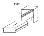
- a printed circuit board 1 is guided in a slide-in housing 2 and this slide-in housing in a superordinate housing insert 9 on each long side with a plastic rail 3 at the same time.
- the guide for the insert forms a continuously rectangular strip 3 which can be fastened in corresponding openings 5 in the side wall 11 of the insert by means of hook-shaped projections 4.
- the hook-shaped approaches are inserted through rectangular openings 5 and inserted up to the stop 6 at the foot of the hook.
- a latching lug 7, which is fastened to at least one end per rail, can additionally be latched into a corresponding opening 8 on the side wall of the housing to secure the position.
- the strip 3 thus initially forms the guide for the slide-in housing 2, which is designed as a closed box according to FIG.
- These rails have corresponding counterparts 10 in the parent housing, into which they can be inserted.
- the higher-level housing is itself, for example, a 7R subrack.
- the hooks are not only present several times on the long sides of the insert, but they are divided in two in the longitudinal direction in such a way that they can accommodate the edge of the circuit board between them.
- the hooks thus simultaneously form the embossments for the plug-in printed circuit board 1.
- both the guide for the printed circuit board and the guide for the insert are realized simultaneously with a relatively simple plastic element that can be produced by injection molding.
- the hooks are expediently beveled in a somewhat funnel shape for better threading of the circuit board in the direction of insertion of the circuit board.
Landscapes
- Engineering & Computer Science (AREA)
- Microelectronics & Electronic Packaging (AREA)
- Mounting Of Printed Circuit Boards And The Like (AREA)
- Coupling Device And Connection With Printed Circuit (AREA)
- Casings For Electric Apparatus (AREA)
Applications Claiming Priority (2)
| Application Number | Priority Date | Filing Date | Title |
|---|---|---|---|
| DE3641210 | 1986-12-03 | ||
| DE3641210 | 1986-12-03 |
Publications (3)
| Publication Number | Publication Date |
|---|---|
| EP0270065A2 true EP0270065A2 (fr) | 1988-06-08 |
| EP0270065A3 EP0270065A3 (en) | 1989-09-06 |
| EP0270065B1 EP0270065B1 (fr) | 1992-02-19 |
Family
ID=6315313
Family Applications (1)
| Application Number | Title | Priority Date | Filing Date |
|---|---|---|---|
| EP87117715A Expired - Lifetime EP0270065B1 (fr) | 1986-12-03 | 1987-11-30 | Tiroir enfichable de télécommunication |
Country Status (3)
| Country | Link |
|---|---|
| EP (1) | EP0270065B1 (fr) |
| JP (1) | JPS63151100A (fr) |
| DE (1) | DE3776768D1 (fr) |
Cited By (3)
| Publication number | Priority date | Publication date | Assignee | Title |
|---|---|---|---|---|
| US4893001A (en) * | 1986-01-20 | 1990-01-09 | Itt Corporation | IC card |
| US5587889A (en) * | 1994-05-17 | 1996-12-24 | Palo Alto Design Group | Edge connector for securing a mountable electronic component to a device with receiving apertures for edge connector |
| GB2344695A (en) * | 1998-12-07 | 2000-06-14 | Alstom Uk Ltd | A housing for an electrical circuit |
Families Citing this family (3)
| Publication number | Priority date | Publication date | Assignee | Title |
|---|---|---|---|---|
| JPH079420Y2 (ja) * | 1989-01-28 | 1995-03-06 | 繁一 河田 | 収納容器 |
| JP2797476B2 (ja) * | 1989-07-11 | 1998-09-17 | 松下電器産業株式会社 | 光磁気メモリ装置 |
| WO2009047851A1 (fr) * | 2007-10-11 | 2009-04-16 | Fujitsu Limited | Structure de montage de rail, procédé de pose/dépose de rail et dispositif électronique |
Family Cites Families (3)
| Publication number | Priority date | Publication date | Assignee | Title |
|---|---|---|---|---|
| CH377902A (de) * | 1960-01-07 | 1964-05-31 | Bbc Brown Boveri & Cie | Apparateeinschubeinheit |
| FR1367798A (fr) * | 1962-07-20 | 1964-07-24 | Sperry Rand Corp | Ensemble connecteur pour panneaux de circuits imprimés |
| DE7716440U1 (de) * | 1977-05-24 | 1977-11-03 | Vero Electronics Gmbh, 2800 Bremen | Führungshalter für Leiterplatten und Kassetten |
-
1987
- 1987-11-30 DE DE8787117715T patent/DE3776768D1/de not_active Expired - Lifetime
- 1987-11-30 EP EP87117715A patent/EP0270065B1/fr not_active Expired - Lifetime
- 1987-12-01 JP JP62301634A patent/JPS63151100A/ja active Pending
Cited By (4)
| Publication number | Priority date | Publication date | Assignee | Title |
|---|---|---|---|---|
| US4893001A (en) * | 1986-01-20 | 1990-01-09 | Itt Corporation | IC card |
| US4909742A (en) * | 1986-01-20 | 1990-03-20 | Itt Corporation | IC card and mating socket |
| US5587889A (en) * | 1994-05-17 | 1996-12-24 | Palo Alto Design Group | Edge connector for securing a mountable electronic component to a device with receiving apertures for edge connector |
| GB2344695A (en) * | 1998-12-07 | 2000-06-14 | Alstom Uk Ltd | A housing for an electrical circuit |
Also Published As
| Publication number | Publication date |
|---|---|
| DE3776768D1 (de) | 1992-03-26 |
| JPS63151100A (ja) | 1988-06-23 |
| EP0270065A3 (en) | 1989-09-06 |
| EP0270065B1 (fr) | 1992-02-19 |
Similar Documents
| Publication | Publication Date | Title |
|---|---|---|
| EP0330957A1 (fr) | Système frontal pour des modules d'un ensemble mécanique enfichables dans une structure support | |
| EP0937317B1 (fr) | Bati electronique pour cartes de circuits avec rails transversaux centraux | |
| EP0194515A1 (fr) | Auxiliaire d'insertion et d'extraction | |
| DE10061940C2 (de) | Kupplungsplatte für Stromschienenadapter | |
| DE19644420C1 (de) | Baugruppenträger | |
| DE3409022C2 (fr) | ||
| EP0270065B1 (fr) | Tiroir enfichable de télécommunication | |
| EP0579859B1 (fr) | Plaque de circuit imprimé avec des tiges de guidage pour l'insérer en position correcte dans un rack électronique | |
| EP0313131A2 (fr) | Dispositif de logement de cartes blindées | |
| DE10013134A1 (de) | Montagerahmen, Verrastungs- und Entriegelungsvorrichtung, insbesondere für einen Montagerahmen, und modulare speicherprogrammierbare Steuerung | |
| DE8632332U1 (de) | Steckeinschub für elektrische Nachrichtentechnik | |
| DE19610037C2 (de) | Baugruppenträger | |
| EP1867021B1 (fr) | Installation de distribution electrique et module de base pour installation de distribution electrique | |
| DE2434892B2 (de) | Gehaeuse fuer elektronische baugruppen | |
| DE1139894B (de) | Einschubrahmen zur Aufnahme mehrerer Schaltungsplatten fuer Fernmeldeanlagen, insbesondere Fernsprechvermittlungsanlagen | |
| DE3412593A1 (de) | Gekapselte baugruppe fuer elektronische baueinheiten | |
| DE3308510A1 (de) | Gehaeuse fuer elektrische und/oder elektronische bauelemente | |
| DE3626852C2 (fr) | ||
| DE3624756C2 (fr) | ||
| EP0062108B1 (fr) | Bâti pour éléments électriques pouvant glisser | |
| EP1102527B1 (fr) | Boîtier protégé contre les décharges électrostatiques | |
| DE3933099A1 (de) | Modulares aufbausystem | |
| EP0217162A1 (fr) | Dispositif pour la fixation de barres de guidage pour constructions intérieures électriques par barre à grille fondamentale normale | |
| DE202024100906U1 (de) | Berührschutzkappe für eine Stromschiene in einem Tragschienensystem | |
| DE3112505C2 (de) | Rahmen für einschiebbare elektrische Baugruppen |
Legal Events
| Date | Code | Title | Description |
|---|---|---|---|
| PUAI | Public reference made under article 153(3) epc to a published international application that has entered the european phase |
Free format text: ORIGINAL CODE: 0009012 |
|
| AK | Designated contracting states |
Kind code of ref document: A2 Designated state(s): DE FR GB IT NL SE |
|
| PUAL | Search report despatched |
Free format text: ORIGINAL CODE: 0009013 |
|
| AK | Designated contracting states |
Kind code of ref document: A3 Designated state(s): DE FR GB IT NL SE |
|
| 17P | Request for examination filed |
Effective date: 19890925 |
|
| 17Q | First examination report despatched |
Effective date: 19910624 |
|
| GRAA | (expected) grant |
Free format text: ORIGINAL CODE: 0009210 |
|
| AK | Designated contracting states |
Kind code of ref document: B1 Designated state(s): DE FR GB IT NL SE |
|
| REF | Corresponds to: |
Ref document number: 3776768 Country of ref document: DE Date of ref document: 19920326 |
|
| ET | Fr: translation filed | ||
| ITF | It: translation for a ep patent filed | ||
| GBT | Gb: translation of ep patent filed (gb section 77(6)(a)/1977) | ||
| PGFP | Annual fee paid to national office [announced via postgrant information from national office to epo] |
Ref country code: GB Payment date: 19921016 Year of fee payment: 6 |
|
| PGFP | Annual fee paid to national office [announced via postgrant information from national office to epo] |
Ref country code: FR Payment date: 19921123 Year of fee payment: 6 |
|
| PGFP | Annual fee paid to national office [announced via postgrant information from national office to epo] |
Ref country code: SE Payment date: 19921125 Year of fee payment: 6 |
|
| PGFP | Annual fee paid to national office [announced via postgrant information from national office to epo] |
Ref country code: NL Payment date: 19921130 Year of fee payment: 6 |
|
| PLBE | No opposition filed within time limit |
Free format text: ORIGINAL CODE: 0009261 |
|
| STAA | Information on the status of an ep patent application or granted ep patent |
Free format text: STATUS: NO OPPOSITION FILED WITHIN TIME LIMIT |
|
| PGFP | Annual fee paid to national office [announced via postgrant information from national office to epo] |
Ref country code: DE Payment date: 19930122 Year of fee payment: 6 |
|
| 26N | No opposition filed | ||
| PG25 | Lapsed in a contracting state [announced via postgrant information from national office to epo] |
Ref country code: GB Effective date: 19931130 |
|
| PG25 | Lapsed in a contracting state [announced via postgrant information from national office to epo] |
Ref country code: SE Effective date: 19931201 |
|
| PG25 | Lapsed in a contracting state [announced via postgrant information from national office to epo] |
Ref country code: NL Effective date: 19940601 |
|
| NLV4 | Nl: lapsed or anulled due to non-payment of the annual fee | ||
| GBPC | Gb: european patent ceased through non-payment of renewal fee |
Effective date: 19931130 |
|
| PG25 | Lapsed in a contracting state [announced via postgrant information from national office to epo] |
Ref country code: FR Effective date: 19940729 |
|
| PG25 | Lapsed in a contracting state [announced via postgrant information from national office to epo] |
Ref country code: DE Effective date: 19940802 |
|
| REG | Reference to a national code |
Ref country code: FR Ref legal event code: ST |
|
| EUG | Se: european patent has lapsed |
Ref document number: 87117715.0 Effective date: 19940710 |
|
| PG25 | Lapsed in a contracting state [announced via postgrant information from national office to epo] |
Ref country code: IT Free format text: LAPSE BECAUSE OF NON-PAYMENT OF DUE FEES;WARNING: LAPSES OF ITALIAN PATENTS WITH EFFECTIVE DATE BEFORE 2007 MAY HAVE OCCURRED AT ANY TIME BEFORE 2007. THE CORRECT EFFECTIVE DATE MAY BE DIFFERENT FROM THE ONE RECORDED. Effective date: 20051130 |