EP0270251A2 - Strahlungs-Darstellungseinrichtung und Verfahren - Google Patents
Strahlungs-Darstellungseinrichtung und Verfahren Download PDFInfo
- Publication number
- EP0270251A2 EP0270251A2 EP87309759A EP87309759A EP0270251A2 EP 0270251 A2 EP0270251 A2 EP 0270251A2 EP 87309759 A EP87309759 A EP 87309759A EP 87309759 A EP87309759 A EP 87309759A EP 0270251 A2 EP0270251 A2 EP 0270251A2
- Authority
- EP
- European Patent Office
- Prior art keywords
- electrodes
- specimen
- plate
- distribution
- detector
- Prior art date
- Legal status (The legal status is an assumption and is not a legal conclusion. Google has not performed a legal analysis and makes no representation as to the accuracy of the status listed.)
- Withdrawn
Links
Images
Classifications
-
- G—PHYSICS
- G02—OPTICS
- G02B—OPTICAL ELEMENTS, SYSTEMS OR APPARATUS
- G02B21/00—Microscopes
- G02B21/0004—Microscopes specially adapted for specific applications
- G02B21/002—Scanning microscopes
-
- G—PHYSICS
- G01—MEASURING; TESTING
- G01T—MEASUREMENT OF NUCLEAR OR X-RADIATION
- G01T1/00—Measuring X-radiation, gamma radiation, corpuscular radiation, or cosmic radiation
- G01T1/29—Measurement performed on radiation beams, e.g. position or section of the beam; Measurement of spatial distribution of radiation
- G01T1/2914—Measurement of spatial distribution of radiation
- G01T1/2921—Static instruments for imaging the distribution of radioactivity in one or two dimensions; Radio-isotope cameras
- G01T1/2928—Static instruments for imaging the distribution of radioactivity in one or two dimensions; Radio-isotope cameras using solid state detectors
Definitions
- This invention relates to a method of imaging and to apparatus for carrying out such method.
- Recent developments in solid state detectors enable the position of radioactive or similar events to be ascertained in two dimensions.
- One example of such a detector is the silicon drift detector, to be described in greater detail below, which briefly comprises a plate-like slab of high purity, high resistivity silicon on which are formed a plurality of parallel spaced strip electrodes and a plurality of anodes arranged along one side. Radioactive particles or photons which pass through the silicon result in the generation of hole-electron pairs which can be directed to adjacent electrodes and anodes to provide an X-Y indication of the position of the passage of the particle or photon.
- a method of imaging utilising imaging apparatus including a semiconductor detector comprising a plate of semiconductor material having a plurality of electrodes on at least one face thereof, and electronic readout circuitry connected to said electrodes in such a way as to enable a signal to be generated upon the passage through the plate of a radioactive particle or photon, said signal being indicative of the spatial position on the plate at which the particle or photon passed through the plate, said method comprising applying to one surface of said plate a specimen in laminar form, whereby the distribution of any radioactive or fluorescent activity within the specimen may be ascertained by analysis of said signal.
- suitable specimens would include thin slices of tissue or suspensions of cells, incorporating radioactive and/or fluorescent labelling.
- the size of the polyacrylamide gel could be cut down to such dimensions as to make it compatible with the present invention, with considerable advantages in speed and convenience, and in the acquisition, storage and processing of the positional information. It is possible also to remove the nucleic acids or proteins from the gel on to a support matrix such as a nitrocellulose sheet ("blotting") where they may be "probed” to establish identity - with "DNA probes” in the case of nucleic acids and with antibodies in the case of proteins, the DNA probe and the antibody being suitably labelled (these processes are known as Southern blotting and Western blotting respectively).
- blotting nitrocellulose sheet
- the specimen support table of a microscope takes the form of a silicon drift detector.
- Means connected to the detector are provided for electronically scanning across the electrodes and anodes of the detector to build up a two-dimensional picture of any radioactive particles or photons issued by the specimen.
- the specimen is labelled with a radioactive label the distribution of radioactivity within the specimen can be displayed on a suitable screen.
- the optical image of the specimen is passed to the eyepiece as usual, but there may additionally be provided a semi-silvered mirror for directing part of the light from the specimen to a video camera, such as a CCD imaging camera, and the resultant image, which can be adjusted to provide the same field of view as that from the semiconductor detector, may be displayed on the aforsaid screen.
- a video camera such as a CCD imaging camera
- the resultant image which can be adjusted to provide the same field of view as that from the semiconductor detector, may be displayed on the aforsaid screen.
- a video camera such as a CCD imaging camera
- the resultant image which can be adjusted to provide the same field of view as that from the semiconductor detector, may be displayed on the aforsaid screen.
- a video camera such as a CCD imaging camera
- the resultant image which can be adjusted to provide the same field of view as that from the semiconductor detector, may be displayed on the aforsaid screen.
- means are provided for allowing "
- a UV source providing a UV beam incident on a fluorescent-labelled specimen
- a video camera view the resultant fluorescent image via a video camera.
- the fluorescent image can likewise be superimposed, added or subtracted from the radioactive and light images.
- means are provided for discriminating between different energy levels in the particles passing through the detector.
- the different images so formed may be pseudo coloured on the screen to enable the viewer to differentiate between several energy levels displayed simultaneously.
- any one specimen may be labelled with several different radioactive labels in order to enable simultaneous viewing of the reaction of the specimen to different chemicals.
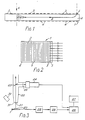
- an exemplary silicon drift detector 1 The detector comprises a plate 23 of high purity n-type silicon cut from a single crystal and typically of 280 ⁇ m thickness. Mounted onto the upper and lower surfaces of the plate 2 by way of rectifying junctions of p+ material such as boron are a plurality of strip electrodes referenced 3 on the upper surface and 4 on the lower surface. The pitch of the electrodes 3 and 4 is typically 20 ⁇ m. Also on the upper surface are a plurality of anodes 5, typically of 40 ⁇ m pitch. The electrodes 3 and 4 and the anodes 5 are connected to associated electronics (not shown) which amplifies and processes signals from the electrodes, which signals are generated by the passage of a radioactive particle or photon through the plate 2, as will be explained later.
- associated electronics not shown
- the operation of the drift detector relies on achieving an electric field distribution within the silicon plate 2 which causes the electrons, once liberated by passage of a particle or photon (see arrow A in Figure 1), to move or "drift" in a rightwards direction along the path indicated by arrow B, eventually to be collected by an anode 5.
- the holes meanwhile flow to the nearest strip electrode 3 and/or 4.
- a current is set up between an anode 5 and one or more strip electrodes 3 or 4.
- the desired electron drift is achieved by correct choice of the potentials on the strip electrodes 3 and 4.
- the electrodes on the top and bottom are in oppositely-disposed pairs; the potentials are arranged such that the electrodes 3 and 4 of each such pair have the same potential so that there is no component of electric field directly across the silicon plate 2.
- Each set of plates is, however, at a different potential to the next, providing a continuous rising or falling potential gradient as one moves along the plate 2.
- the anode 5, for example might be at ground potential, with the next adjacent strip electrode 3 and its corresponding opposite electrode 4 at a negative potential of 100 volts.
- the next pair 3, 4 of strip electrodes will have a higher negative potential, say 110 volts, and so on to the left-hand end of the detector.
- the electric field distribution which results acts effectively as a sloping "gutter", positioned along the centre of the silicon plate, along which liberated electrons flow from left to right in Figure 1.
- the field distribution is distorted in such a way as to cause the electrons to flow into the anode, as mentioned above.
- drift detector can be configured as a multi-anode detector, enabling detection of events in two dimensions. This is illustrated diagrammatically in Figure 2 which is a view of the top surface showing only the strip electrodes 3 (the electrodes 4 being hidden), together with a plurality of anodes 5.
- the spatial resolution obtained from the detector is dependent upon the pitch of the electrodes and anodes and also upon the manner in which the electrodes are connected to the associated readout circuitry.
- a resolution of 3 ⁇ m is obtainable with an inter-electrode pitch of 20 ⁇ m along the axis at right angles to the electrodes 3 and 4; in the orthogonal axis, with an inter-anode pitch of 40 ⁇ m, a resolution of 6 ⁇ m is obtainable.
- the present invention utilises a detector such as described above to obtain a two-dimensional map of the distribution of radioactivity or fluorescence in a specimen.
- This may be achieved simply by placing a suitably labelled specimen directly onto the top or bottom surface of the detector, possibly with a thin protective layer inbetween.
- the readout electronics will produce a signal which may for example be displayed on a computer screen which delineates the distribution of the radioactive or fluorescent label within the specimen. It is however more convenient to be able to simultaneously view a conventional optical image of the specimen at the same time as the distribution of the label. This enables the operator to assess the distribution of label by reference to the physical features of the specimen. This can be achieved by incorporating a detector 1 as the bed of a microscope.
- FIG. 3 there is shown a microscope apparatus incorporating a detector 1 as a support for a specimen 20.
- Light 21 reflected from the specimen passes into the microscope optics (not shown) within the microscope column 22 and to the eyepiece.
- a semi-silvered mirror 23 intercepts some of the light and passes it to a video camera 24, optionally via a filter 25.
- the output from the video camera is passed, after appropriate signal processing, to a computer 26 having a screen display 27.
- the various outputs from the detector 1 are passed to detection electronics 28 which is operable to amplify the signals from the electrodes and anodes of the detector and pass them to respective sample and hold circuits within the detection electronics.
- Scanning means 29 are used to cycle round or scan the outputs to achieve a serial signal on a single line which is then passed, again after appropriate signal processing, to the computer 26.
- An optional UV source 30 generates a UV beam 31 which is incident on the specimen 20 and may likewise provide a picture in the camera 24 if the specimen is labelled with a fluorescent label.
- the above described apparatus enables the simultaneous viewing of optical, radioactive and/or fluorescent images of a suitably labelled specimen such as a tissue section, a mini electrophoretogram or the "blot" prepared from it.
- a suitably labelled specimen such as a tissue section, a mini electrophoretogram or the "blot" prepared from it.
- the detection electronics 28 is equipped with amplitude discrimination facilities, specimens labelled with different energy isotopes can be imaged simultaneously.
- a specimen labelled both with sulphur-35 and phosphorous-32 can produce separate images which can be simultaneously displayed, together with the optical and possibly the fluorescent images as well.
- the images can alternatively be combined in various ways, for example by addition or subtraction, to give different effects necessary to visually analyse the specimen.
- Pseudo-colours can also be generated by manipulation of the grey scales.
- the detector 1 effectively provides a map of the distribution of radioactivity within the specimen which can be compared with a corresponding optical and/or fluorescent image of the specimen. This enables the pattern of radioactivity within the specimen to be directly correlated with the physical features of the specimen.
Landscapes
- Physics & Mathematics (AREA)
- General Physics & Mathematics (AREA)
- Spectroscopy & Molecular Physics (AREA)
- Life Sciences & Earth Sciences (AREA)
- High Energy & Nuclear Physics (AREA)
- Molecular Biology (AREA)
- Health & Medical Sciences (AREA)
- Chemical & Material Sciences (AREA)
- Analytical Chemistry (AREA)
- Optics & Photonics (AREA)
- Investigating, Analyzing Materials By Fluorescence Or Luminescence (AREA)
- Measurement Of Radiation (AREA)
- Radiography Using Non-Light Waves (AREA)
Applications Claiming Priority (2)
| Application Number | Priority Date | Filing Date | Title |
|---|---|---|---|
| GB868626576A GB8626576D0 (en) | 1986-11-06 | 1986-11-06 | Imaging method |
| GB8626576 | 1986-11-06 |
Publications (2)
| Publication Number | Publication Date |
|---|---|
| EP0270251A2 true EP0270251A2 (de) | 1988-06-08 |
| EP0270251A3 EP0270251A3 (de) | 1988-07-13 |
Family
ID=10606918
Family Applications (1)
| Application Number | Title | Priority Date | Filing Date |
|---|---|---|---|
| EP87309759A Withdrawn EP0270251A3 (de) | 1986-11-06 | 1987-11-04 | Strahlungs-Darstellungseinrichtung und Verfahren |
Country Status (4)
| Country | Link |
|---|---|
| EP (1) | EP0270251A3 (de) |
| JP (1) | JPS63148191A (de) |
| AU (1) | AU8080387A (de) |
| GB (1) | GB8626576D0 (de) |
Cited By (3)
| Publication number | Priority date | Publication date | Assignee | Title |
|---|---|---|---|---|
| EP0383389A1 (de) * | 1989-02-13 | 1990-08-22 | Technische Universiteit Delft | Lageempfindlicher Strahlungsdetektor |
| WO1992002839A1 (en) * | 1990-08-10 | 1992-02-20 | Regents Of The University Of Minnesota | Laser for confocal microscope |
| WO1997034995A1 (en) * | 1996-03-18 | 1997-09-25 | Marine Biological Laboratory | Analytical imaging system and process |
Family Cites Families (2)
| Publication number | Priority date | Publication date | Assignee | Title |
|---|---|---|---|---|
| GB1344703A (en) * | 1970-07-08 | 1974-01-23 | Ceskoslovenska Akademie Ved | Method for determination of the planar distribution of low- energy beta nuclides or other radionuclides for tracer experiments |
| US4045673A (en) * | 1976-05-12 | 1977-08-30 | The United States Of America As Represented By The United States Energy Research And Development Administration | Test chamber for alpha spectrometry |
-
1986
- 1986-11-06 GB GB868626576A patent/GB8626576D0/en active Pending
-
1987
- 1987-11-04 EP EP87309759A patent/EP0270251A3/de not_active Withdrawn
- 1987-11-05 AU AU80803/87A patent/AU8080387A/en not_active Abandoned
- 1987-11-06 JP JP62280835A patent/JPS63148191A/ja active Pending
Cited By (6)
| Publication number | Priority date | Publication date | Assignee | Title |
|---|---|---|---|---|
| EP0383389A1 (de) * | 1989-02-13 | 1990-08-22 | Technische Universiteit Delft | Lageempfindlicher Strahlungsdetektor |
| US5051801A (en) * | 1989-02-13 | 1991-09-24 | Technische Universiteit Delft | Position-sensitive radiation detector |
| WO1992002839A1 (en) * | 1990-08-10 | 1992-02-20 | Regents Of The University Of Minnesota | Laser for confocal microscope |
| US5127730A (en) * | 1990-08-10 | 1992-07-07 | Regents Of The University Of Minnesota | Multi-color laser scanning confocal imaging system |
| WO1997034995A1 (en) * | 1996-03-18 | 1997-09-25 | Marine Biological Laboratory | Analytical imaging system and process |
| US6078681A (en) * | 1996-03-18 | 2000-06-20 | Marine Biological Laboratory | Analytical imaging system and process |
Also Published As
| Publication number | Publication date |
|---|---|
| GB8626576D0 (en) | 1986-12-10 |
| AU8080387A (en) | 1988-05-12 |
| JPS63148191A (ja) | 1988-06-21 |
| EP0270251A3 (de) | 1988-07-13 |
Similar Documents
| Publication | Publication Date | Title |
|---|---|---|
| US6103533A (en) | Molecular imaging | |
| US5366608A (en) | Electrophoresis gel migration apparatus | |
| US7199357B1 (en) | Image enhancement by sub-pixel imaging | |
| EP1446676B1 (de) | Elektronenstrahl-abbildungssystem mit einem punktgitterarray | |
| US7323681B1 (en) | Image enhancement by sub-pixel imaging | |
| US10788423B2 (en) | Image capture for large analyte arrays | |
| RU94028284A (ru) | Способ фотонной сканирующей туннельной микроскопии и фотонный сканирующий туннельный микроскоп | |
| US6752914B1 (en) | Capillary electrophoresis device | |
| US4884200A (en) | Signal detecting method in autoradiography | |
| EP0270251A2 (de) | Strahlungs-Darstellungseinrichtung und Verfahren | |
| US5969361A (en) | Transparent position-sensitive particle detector | |
| US6800438B2 (en) | Imager for DNA sequencer | |
| EP0268406A2 (de) | Gerät zur biochemischen Sequenzanalyse | |
| Sakai et al. | Development of a fast multi-parameter data acquisition system for microbeam analyses | |
| EP0886791B1 (de) | Autoradiographische aufzeichnung | |
| US20040120459A1 (en) | Industrial machine vision system having a direct conversion X-ray detector | |
| Abate et al. | GaAs pixel arrays for β imaging in medicine and biology | |
| Tousignant et al. | Energy and position resolution of a CdZnTe gamma-ray detector with orthogonal coplanar anodes | |
| Sutherland | Electronic imaging systems for quantitative electrophoresis of DNA | |
| Ledley et al. | SPIDAC: specimen input to digital automatic computer | |
| JP2003329622A (ja) | X線撮像装置および方法 | |
| Eggers et al. | A versatile biochip for gene-based diagnostics | |
| Sutherland | Electronic imaging systems for quantitative electrophoresis of DNA | |
| JPH11510246A (ja) | 位置に感じ易い粒子検出器及び透明体 | |
| Karchin | An inexpensive microscope television for the detection and measurement of nuclear emulsion tracks |
Legal Events
| Date | Code | Title | Description |
|---|---|---|---|
| PUAI | Public reference made under article 153(3) epc to a published international application that has entered the european phase |
Free format text: ORIGINAL CODE: 0009012 |
|
| PUAL | Search report despatched |
Free format text: ORIGINAL CODE: 0009013 |
|
| AK | Designated contracting states |
Kind code of ref document: A2 Designated state(s): AT BE CH DE ES FR GB IT LI LU NL SE |
|
| AK | Designated contracting states |
Kind code of ref document: A3 Designated state(s): AT BE CH DE ES FR GB IT LI LU NL SE |
|
| 17P | Request for examination filed |
Effective date: 19880816 |
|
| 17Q | First examination report despatched |
Effective date: 19891201 |
|
| STAA | Information on the status of an ep patent application or granted ep patent |
Free format text: STATUS: THE APPLICATION IS DEEMED TO BE WITHDRAWN |
|
| 18D | Application deemed to be withdrawn |
Effective date: 19900412 |
|
| RIN1 | Information on inventor provided before grant (corrected) |
Inventor name: FINLAN, MARTIN FRANCIS Inventor name: BRADY, MICHAEL ANTHONY WARBURTON |