EP0271932A2 - Cellule mémoire EEPROM ayant deux niveaux de polysilicium et une zone d'oxyde tunnel - Google Patents
Cellule mémoire EEPROM ayant deux niveaux de polysilicium et une zone d'oxyde tunnel Download PDFInfo
- Publication number
- EP0271932A2 EP0271932A2 EP87202038A EP87202038A EP0271932A2 EP 0271932 A2 EP0271932 A2 EP 0271932A2 EP 87202038 A EP87202038 A EP 87202038A EP 87202038 A EP87202038 A EP 87202038A EP 0271932 A2 EP0271932 A2 EP 0271932A2
- Authority
- EP
- European Patent Office
- Prior art keywords
- gate
- transistor
- polysilicon
- memory cell
- pickup
- Prior art date
- Legal status (The legal status is an assumption and is not a legal conclusion. Google has not performed a legal analysis and makes no representation as to the accuracy of the status listed.)
- Withdrawn
Links
Images

Classifications
-
- H—ELECTRICITY
- H10—SEMICONDUCTOR DEVICES; ELECTRIC SOLID-STATE DEVICES NOT OTHERWISE PROVIDED FOR
- H10D—INORGANIC ELECTRIC SEMICONDUCTOR DEVICES
- H10D30/00—Field-effect transistors [FET]
- H10D30/60—Insulated-gate field-effect transistors [IGFET]
- H10D30/68—Floating-gate IGFETs
- H10D30/681—Floating-gate IGFETs having only two programming levels
- H10D30/683—Floating-gate IGFETs having only two programming levels programmed by tunnelling of carriers, e.g. Fowler-Nordheim tunnelling
-
- H—ELECTRICITY
- H10—SEMICONDUCTOR DEVICES; ELECTRIC SOLID-STATE DEVICES NOT OTHERWISE PROVIDED FOR
- H10B—ELECTRONIC MEMORY DEVICES
- H10B69/00—Erasable-and-programmable ROM [EPROM] devices not provided for in groups H10B41/00 - H10B63/00, e.g. ultraviolet erasable-and-programmable ROM [UVEPROM] devices
Definitions
- the present invention relates to an EEPROM memory cell with two levels of polysilicon programmable for a Fowler-Nordheim tunnel through a thin oxide zone.
- Cells of this type are known to comprise a zone of thin oxide or tunnel oxide placed between a selection transistor and a pickup transistor.
- a first layer of polysilicon forms the gate of the selection transistor and separately a floating gate superimposed on the thin oxide zone and accomplished in a single piece with a first gate of the pickup transistor.
- a second layer of polysilicon superimposed on the first by interposing insulating oxide forms the common control gate for the thin oxide zone and the pickup transistor.
- the object of the present invention is to achieve an EEPROM memory cell with two levels of polysilicon and tunnel oxide zones which would present greater compactness and technological simplicity while maintaining intact the reliability characteristics of the conventional cells of the same type.
- an EEPROM cell comprising a selection transistor, a pickup transistor, a thin oxide zone, a floating gate superimposed on said thin oxide zone and made with a first layer of polysilicon in a single piece with a first gate of the pickup transistor, and a control gate superimposed on said first gate of the pickup transistor and made with a second layer of polysilicon characterized in that said second layer of polysilicon also forms in a single piece the gate of the selection transistor.
- the EEPROM cell in accordance with the present invention does not provide the selection transistor as an element separate from the others but utilizes for its functions a portion of the second polysilicon layer, i.e. of the control gate.
- the memory cell in accordance with the invention can thus be made more simply and in a more compact form.
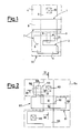
- FIG. 1 With reference to FIG. 1 there is illustrated an EEPROM memory cell in accordance with the known art which comprises a selection tansistor 1, a pickup transistor 2 and a tunnel area 3 placed between the two transistors.
- an active area 5 presenting a thin oxide or tunnel oxide zone 6.
- a gate oxide on which is deposited a first layer of polysilicon or polycrystalline silicon 7 formed by a straight strip 8 defining the gate of the selection transistor 1 and separately a C-shaped strip 9 a branch 10 of which defines the floating gate of the tunnel area 3 while the other arm 11 defines a first gate of the pickup transistor 2.
- a second layer of polysilicon 12 in the form of a straight strip is placed above said first polysilicon strip 9 (with interposed insulating oxide) to define the control gate for the pickup transistor 2 and the tunnel area 3.
- Reference number 13 indicates the drain contact of the memory cell shifted axially in relation to the selection transistor 51.
- FIGS. 2-4 illustrate an EEPROM memory cell in accordance with the invention in which the selection transistor is indicated with reference number 51, the pickup transistor is indicated with reference number 52 and the tunnel area is indicated with reference number 53.
- the selection transistor 51 and the pickup transistor 52 are side-by-side while the tunnel area is shifted sidewise in relation to the two transistors.
- an active area 55 presenting a thin oxide or tunnel oxide zone 56 (FIGS. 2 and 4).
- a gate oxide 66 on which is deposited a first layer of polysilicon or polycrystalline silicon 57 formed of a laterally shifted axial branch 58 defining the floating gate of the tunnel area 53 and a transversal arm 59 defining a first gate of the pickup transistor 52 and having a central cavity 60.
- a second polysilicon layer 61 in the form of a straight strip is placed over said transverse arm 59 of the first polysilicon layer 57 (with interposed insulating oxide 62 also placed over the floating gate 58) to define the control gate of the pickup transistor 52 and, inside the cavity 60, the gate of the selection transistor 51 (FIGS. 2 and 3).
- Reference number 63 indicates the drain contact of the memory cell moved axially in relation to the transistors 51 and 52 but beside the tunnel area 53.
- Reference number 65 indicates the output contact of said memory cell.
- the EEPROM memory cell illustated in FIGS. 2-4 is capable of operating as follows.
- the drain contact 63 is placed at a high level while the second polysilicon layer 61 is grounded. In this manner the selection transistor 51 is estinguished and no axial current passes so that the drain contact 63 remains high. Furthermore, due to the effect of the capacitive couplings connected to the floating gate 58 and the control gate 61, voltage is discharged from the drain contact 63 on the floating gate 58, removing electrons from the latter and in this manner performing the 'writing' of the cell. Thanks to the pickup transistor 52 current passes between the two contacts 63 and 65.
- the second polysilicon layer 61 is brought to high voltage while the drain contact 63 is grounded.
- the voltage is thus divided between the second polysilicon layer 61 and the drain contact 63 through the various capacitive couplings so that the floating gate 58 is charged with electrons and the pickup transistor 52 remains extinguished.
- control gate of the selection transistor 51 is brought to a voltage higher than its operating theshhold so as to open the electrical path of the drain contact 63 to the pickup transistor 52.
- the cell thus formed lends itself to the simultaneous writing of an entire column of memory cells, since the high level of the drain contact 63 tends in any case to affect the other cells of the same column.
Landscapes
- Non-Volatile Memory (AREA)
Applications Claiming Priority (2)
| Application Number | Priority Date | Filing Date | Title |
|---|---|---|---|
| IT2237286 | 1986-11-18 | ||
| IT22372/86A IT1198108B (it) | 1986-11-18 | 1986-11-18 | Cella di memori aeeprom a due livelli di polisilicio con zona di ossiso di tunnel |
Publications (2)
| Publication Number | Publication Date |
|---|---|
| EP0271932A2 true EP0271932A2 (fr) | 1988-06-22 |
| EP0271932A3 EP0271932A3 (fr) | 1988-12-07 |
Family
ID=11195368
Family Applications (1)
| Application Number | Title | Priority Date | Filing Date |
|---|---|---|---|
| EP87202038A Withdrawn EP0271932A3 (fr) | 1986-11-18 | 1987-10-23 | Cellule mémoire EEPROM ayant deux niveaux de polysilicium et une zone d'oxyde tunnel |
Country Status (3)
| Country | Link |
|---|---|
| EP (1) | EP0271932A3 (fr) |
| JP (1) | JPS63136572A (fr) |
| IT (1) | IT1198108B (fr) |
Cited By (4)
| Publication number | Priority date | Publication date | Assignee | Title |
|---|---|---|---|---|
| EP0367152A3 (fr) * | 1988-11-01 | 1990-11-07 | Casio Computer Company Limited | Dispositif de mémoire utilisant des transistors à couche mince ayant une fonction mémoire et méthode pour les fabriquer |
| US7859043B2 (en) | 2008-02-25 | 2010-12-28 | Tower Semiconductor Ltd. | Three-terminal single poly NMOS non-volatile memory cell |
| US7948020B2 (en) | 2008-02-25 | 2011-05-24 | Tower Semiconductor Ltd. | Asymmetric single poly NMOS non-volatile memory cell |
| US8344440B2 (en) | 2008-02-25 | 2013-01-01 | Tower Semiconductor Ltd. | Three-terminal single poly NMOS non-volatile memory cell with shorter program/erase times |
Family Cites Families (4)
| Publication number | Priority date | Publication date | Assignee | Title |
|---|---|---|---|---|
| JPS5292441A (en) * | 1976-01-30 | 1977-08-03 | Toshiba Corp | Semiconductor memory unit |
| DE2743422A1 (de) * | 1977-09-27 | 1979-03-29 | Siemens Ag | Wortweise loeschbarer, nicht fluechtiger speicher in floating-gate-technik |
| US4479203A (en) * | 1981-11-16 | 1984-10-23 | Motorola, Inc. | Electrically erasable programmable read only memory cell |
| JPS59121880A (ja) * | 1982-12-28 | 1984-07-14 | Toshiba Corp | 不揮発性半導体記憶装置 |
-
1986
- 1986-11-18 IT IT22372/86A patent/IT1198108B/it active
-
1987
- 1987-10-23 EP EP87202038A patent/EP0271932A3/fr not_active Withdrawn
- 1987-11-17 JP JP62288599A patent/JPS63136572A/ja active Pending
Cited By (5)
| Publication number | Priority date | Publication date | Assignee | Title |
|---|---|---|---|---|
| EP0367152A3 (fr) * | 1988-11-01 | 1990-11-07 | Casio Computer Company Limited | Dispositif de mémoire utilisant des transistors à couche mince ayant une fonction mémoire et méthode pour les fabriquer |
| US5060034A (en) * | 1988-11-01 | 1991-10-22 | Casio Computer Co., Ltd. | Memory device using thin film transistors having an insulation film with si/n composition ratio of 0.85 to 1.1 |
| US7859043B2 (en) | 2008-02-25 | 2010-12-28 | Tower Semiconductor Ltd. | Three-terminal single poly NMOS non-volatile memory cell |
| US7948020B2 (en) | 2008-02-25 | 2011-05-24 | Tower Semiconductor Ltd. | Asymmetric single poly NMOS non-volatile memory cell |
| US8344440B2 (en) | 2008-02-25 | 2013-01-01 | Tower Semiconductor Ltd. | Three-terminal single poly NMOS non-volatile memory cell with shorter program/erase times |
Also Published As
| Publication number | Publication date |
|---|---|
| EP0271932A3 (fr) | 1988-12-07 |
| IT1198108B (it) | 1988-12-21 |
| JPS63136572A (ja) | 1988-06-08 |
| IT8622372A0 (it) | 1986-11-18 |
Similar Documents
| Publication | Publication Date | Title |
|---|---|---|
| US5656839A (en) | Semiconductor integrated circuit device having single-element type nonvolatile memory elements | |
| US4754320A (en) | EEPROM with sidewall control gate | |
| EP0037201B1 (fr) | Dispositif de mémoire à MOSFET électriquement effaçable | |
| US4209849A (en) | Non-volatile memory which can be erased word by word constructed in the floating gate technique | |
| EP0044384B1 (fr) | Cellule de mémoire non-volatile électriquement modifiable | |
| US4412311A (en) | Storage cell for nonvolatile electrically alterable memory | |
| EP0272732B1 (fr) | Cellule mémoire EEPROM ayant une seule couche de polysilicium programmable et effaçable bit par bit | |
| KR0147452B1 (ko) | 불휘발성 반도체기억장치 | |
| US4823316A (en) | Eeprom memory cell with a single polysilicon level and a tunnel oxide zone | |
| US5892709A (en) | Single level gate nonvolatile memory device and method for accessing the same | |
| JPH0130315B2 (fr) | ||
| JPS5951753B2 (ja) | 高効率の不揮発性eprom | |
| US4573144A (en) | Common floating gate programmable link | |
| JPS60177678A (ja) | 半導体集積回路装置の製造方法 | |
| JPS62291180A (ja) | 電気的に変更できる持久記憶浮動ゲ−トメモリデバイス | |
| US5371027A (en) | Method of manufacturing a semiconductor device having a non-volatile memory with an improved tunnel oxide | |
| IE50819B1 (en) | Semiconductor storage cell | |
| EP0271932A2 (fr) | Cellule mémoire EEPROM ayant deux niveaux de polysilicium et une zone d'oxyde tunnel | |
| US4586065A (en) | MNOS memory cell without sidewalk | |
| EP0244367A2 (fr) | Dispositif intégré à semi-conducteur du type MOS avec une grille d'oxyde non uniforme et procédé pour sa fabrication | |
| EP0432792A2 (fr) | Dispositif de mémoire non volatile à semi-conducteur et son procédé de fabrication | |
| US6221717B1 (en) | EEPROM memory cell comprising a selection transistor with threshold voltage adjusted by implantation, and related manufacturing process | |
| JPH032352B2 (fr) | ||
| JPS62125677A (ja) | 半導体装置及びその製造方法 | |
| US5859455A (en) | Non-volatile semiconductor memory cell with control gate and floating gate and select gate located above the channel |
Legal Events
| Date | Code | Title | Description |
|---|---|---|---|
| PUAI | Public reference made under article 153(3) epc to a published international application that has entered the european phase |
Free format text: ORIGINAL CODE: 0009012 |
|
| AK | Designated contracting states |
Kind code of ref document: A2 Designated state(s): DE FR GB NL |
|
| PUAL | Search report despatched |
Free format text: ORIGINAL CODE: 0009013 |
|
| RHK1 | Main classification (correction) |
Ipc: H01L 29/78 |
|
| AK | Designated contracting states |
Kind code of ref document: A3 Designated state(s): DE FR GB NL |
|
| STAA | Information on the status of an ep patent application or granted ep patent |
Free format text: STATUS: THE APPLICATION IS DEEMED TO BE WITHDRAWN |
|
| 18D | Application deemed to be withdrawn |
Effective date: 19890701 |
|
| RIN1 | Information on inventor provided before grant (corrected) |
Inventor name: RIVA, CARLO |