EP0272046A2 - Schaltungsstruktur mit einem gemischten keramischen Substrat - Google Patents
Schaltungsstruktur mit einem gemischten keramischen Substrat Download PDFInfo
- Publication number
- EP0272046A2 EP0272046A2 EP87310837A EP87310837A EP0272046A2 EP 0272046 A2 EP0272046 A2 EP 0272046A2 EP 87310837 A EP87310837 A EP 87310837A EP 87310837 A EP87310837 A EP 87310837A EP 0272046 A2 EP0272046 A2 EP 0272046A2
- Authority
- EP
- European Patent Office
- Prior art keywords
- recess
- layers
- electrically conductive
- ceramic
- arrangement
- Prior art date
- Legal status (The legal status is an assumption and is not a legal conclusion. Google has not performed a legal analysis and makes no representation as to the accuracy of the status listed.)
- Withdrawn
Links
Images
Classifications
-
- H—ELECTRICITY
- H10—SEMICONDUCTOR DEVICES; ELECTRIC SOLID-STATE DEVICES NOT OTHERWISE PROVIDED FOR
- H10W—GENERIC PACKAGES, INTERCONNECTIONS, CONNECTORS OR OTHER CONSTRUCTIONAL DETAILS OF DEVICES COVERED BY CLASS H10
- H10W70/00—Package substrates; Interposers; Redistribution layers [RDL]
- H10W70/01—Manufacture or treatment
- H10W70/05—Manufacture or treatment of insulating or insulated package substrates, or of interposers, or of redistribution layers
-
- H—ELECTRICITY
- H10—SEMICONDUCTOR DEVICES; ELECTRIC SOLID-STATE DEVICES NOT OTHERWISE PROVIDED FOR
- H10W—GENERIC PACKAGES, INTERCONNECTIONS, CONNECTORS OR OTHER CONSTRUCTIONAL DETAILS OF DEVICES COVERED BY CLASS H10
- H10W70/00—Package substrates; Interposers; Redistribution layers [RDL]
- H10W70/60—Insulating or insulated package substrates; Interposers; Redistribution layers
- H10W70/611—Insulating or insulated package substrates; Interposers; Redistribution layers for connecting multiple chips together
-
- H—ELECTRICITY
- H10—SEMICONDUCTOR DEVICES; ELECTRIC SOLID-STATE DEVICES NOT OTHERWISE PROVIDED FOR
- H10W—GENERIC PACKAGES, INTERCONNECTIONS, CONNECTORS OR OTHER CONSTRUCTIONAL DETAILS OF DEVICES COVERED BY CLASS H10
- H10W70/00—Package substrates; Interposers; Redistribution layers [RDL]
- H10W70/60—Insulating or insulated package substrates; Interposers; Redistribution layers
- H10W70/67—Insulating or insulated package substrates; Interposers; Redistribution layers characterised by their insulating layers or insulating parts
- H10W70/68—Shapes or dispositions thereof
- H10W70/685—Shapes or dispositions thereof comprising multiple insulating layers
-
- H—ELECTRICITY
- H10—SEMICONDUCTOR DEVICES; ELECTRIC SOLID-STATE DEVICES NOT OTHERWISE PROVIDED FOR
- H10W—GENERIC PACKAGES, INTERCONNECTIONS, CONNECTORS OR OTHER CONSTRUCTIONAL DETAILS OF DEVICES COVERED BY CLASS H10
- H10W70/00—Package substrates; Interposers; Redistribution layers [RDL]
- H10W70/60—Insulating or insulated package substrates; Interposers; Redistribution layers
- H10W70/67—Insulating or insulated package substrates; Interposers; Redistribution layers characterised by their insulating layers or insulating parts
- H10W70/68—Shapes or dispositions thereof
- H10W70/682—Shapes or dispositions thereof comprising holes having chips therein
-
- H—ELECTRICITY
- H10—SEMICONDUCTOR DEVICES; ELECTRIC SOLID-STATE DEVICES NOT OTHERWISE PROVIDED FOR
- H10W—GENERIC PACKAGES, INTERCONNECTIONS, CONNECTORS OR OTHER CONSTRUCTIONAL DETAILS OF DEVICES COVERED BY CLASS H10
- H10W72/00—Interconnections or connectors in packages
- H10W72/071—Connecting or disconnecting
- H10W72/075—Connecting or disconnecting of bond wires
- H10W72/07551—Connecting or disconnecting of bond wires characterised by changes in properties of the bond wires during the connecting
- H10W72/07554—Connecting or disconnecting of bond wires characterised by changes in properties of the bond wires during the connecting changes in dispositions
-
- H—ELECTRICITY
- H10—SEMICONDUCTOR DEVICES; ELECTRIC SOLID-STATE DEVICES NOT OTHERWISE PROVIDED FOR
- H10W—GENERIC PACKAGES, INTERCONNECTIONS, CONNECTORS OR OTHER CONSTRUCTIONAL DETAILS OF DEVICES COVERED BY CLASS H10
- H10W72/00—Interconnections or connectors in packages
- H10W72/50—Bond wires
- H10W72/541—Dispositions of bond wires
- H10W72/5449—Dispositions of bond wires not being orthogonal to a side surface of the chip, e.g. fan-out arrangements
-
- H—ELECTRICITY
- H10—SEMICONDUCTOR DEVICES; ELECTRIC SOLID-STATE DEVICES NOT OTHERWISE PROVIDED FOR
- H10W—GENERIC PACKAGES, INTERCONNECTIONS, CONNECTORS OR OTHER CONSTRUCTIONAL DETAILS OF DEVICES COVERED BY CLASS H10
- H10W72/00—Interconnections or connectors in packages
- H10W72/50—Bond wires
- H10W72/541—Dispositions of bond wires
- H10W72/547—Dispositions of multiple bond wires
-
- H—ELECTRICITY
- H10—SEMICONDUCTOR DEVICES; ELECTRIC SOLID-STATE DEVICES NOT OTHERWISE PROVIDED FOR
- H10W—GENERIC PACKAGES, INTERCONNECTIONS, CONNECTORS OR OTHER CONSTRUCTIONAL DETAILS OF DEVICES COVERED BY CLASS H10
- H10W72/00—Interconnections or connectors in packages
- H10W72/50—Bond wires
- H10W72/551—Materials of bond wires
- H10W72/552—Materials of bond wires comprising metals or metalloids, e.g. silver
- H10W72/5522—Materials of bond wires comprising metals or metalloids, e.g. silver comprising gold [Au]
Definitions
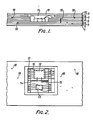
- the present invention seeks to provide an improved circuit arrangement.
- the apertures in the flexible substrates can be formed before or after the formation of the electrically conductive patterns. In order to increase the effective thickness of a part of the composite structure, some of the apertured structures can be produced without conductive layers. Alternatively, substrates of different thicknesses could be used, but it is more convenient to fabricate the circuit arrangement from flexible ceramic substrates all having the same thickness.
- the electrically conductive patterns are formed of conductive inks printed through an appropriately patterned screen mesh.
- screen printing techniques on a flexible ceramic substrate permits fine patterns and closely controlled geometry to be readily achieved.
- each semiconductor device comprises an integrated circuit having a large number of electronic elements, eg field effect transistors, which cooperate to constitute a gate array or the like. These devices are preferably connected to the composite structure by means of bonded gold wires.
- the composite structure is heated to a high temperature of about 800°C so as to completely fire the ceramic material and to burn off any remaining organic materials present.
- the layers of ceramic material which typically is largely alumina, form a single unitary rigid plate which is chemically inert.
Landscapes
- Production Of Multi-Layered Print Wiring Board (AREA)
Applications Claiming Priority (2)
| Application Number | Priority Date | Filing Date | Title |
|---|---|---|---|
| GB8630314 | 1986-12-18 | ||
| GB08630314A GB2199182A (en) | 1986-12-18 | 1986-12-18 | Multilayer circuit arrangement |
Publications (2)
| Publication Number | Publication Date |
|---|---|
| EP0272046A2 true EP0272046A2 (de) | 1988-06-22 |
| EP0272046A3 EP0272046A3 (de) | 1988-09-28 |
Family
ID=10609247
Family Applications (1)
| Application Number | Title | Priority Date | Filing Date |
|---|---|---|---|
| EP87310837A Withdrawn EP0272046A3 (de) | 1986-12-18 | 1987-12-09 | Schaltungsstruktur mit einem gemischten keramischen Substrat |
Country Status (2)
| Country | Link |
|---|---|
| EP (1) | EP0272046A3 (de) |
| GB (1) | GB2199182A (de) |
Cited By (10)
| Publication number | Priority date | Publication date | Assignee | Title |
|---|---|---|---|---|
| FR2649851A1 (fr) * | 1989-07-15 | 1991-01-18 | Diehl Gmbh & Co | Disposition d'un circuit integre sur un support de circuit |
| EP0359416A3 (de) * | 1988-09-16 | 1991-06-12 | Stc Plc | Hybridschaltungen |
| EP0441180A1 (de) * | 1989-01-09 | 1991-08-14 | Mitsubishi Denki Kabushiki Kaisha | Mikrowellenschaltungselemente enthaltende integrierte Schaltungsanordnung |
| US5136271A (en) * | 1989-01-09 | 1992-08-04 | Mitsubishi Denki Kabushiki Kaisha | Microwave integrated circuit mountings |
| US5177668A (en) * | 1989-07-15 | 1993-01-05 | Diehl Gmbh & Co. | Arrangement of an integrated circuit on a circuit board |
| EP0597144A1 (de) * | 1992-11-12 | 1994-05-18 | IXYS Semiconductor GmbH | Hybride leistungselektronische Anordnung |
| EP0695631A1 (de) * | 1994-07-28 | 1996-02-07 | International Business Machines Corporation | Verfahren zum Herstellen keramischer Mehrschichtsubstrate mit zentraler Öffnung |
| GB2293918A (en) * | 1994-10-06 | 1996-04-10 | Ibm | Electronic circuit packaging |
| DE19631046B4 (de) * | 1996-08-01 | 2004-01-29 | Diehl Stiftung & Co. | Bond-Struktur |
| EP2339624A3 (de) * | 2009-10-23 | 2011-10-05 | Electronics and Telecommunications Research Institute | Mehrschichtige Verbindungsstruktur und Herstellungsverfahren dafür |
Families Citing this family (8)
| Publication number | Priority date | Publication date | Assignee | Title |
|---|---|---|---|---|
| DE4115043A1 (de) * | 1991-05-08 | 1997-07-17 | Gen Electric | Dichtgepackte Verbindungsstruktur, die eine Kammer enthält |
| GB2279803B (en) * | 1990-04-05 | 1995-05-24 | Gen Electric | A high density interconnect structure including a chamber |
| US5490324A (en) * | 1993-09-15 | 1996-02-13 | Lsi Logic Corporation | Method of making integrated circuit package having multiple bonding tiers |
| US5384689A (en) * | 1993-12-20 | 1995-01-24 | Shen; Ming-Tung | Integrated circuit chip including superimposed upper and lower printed circuit boards |
| JP3014029B2 (ja) * | 1995-06-16 | 2000-02-28 | 日本電気株式会社 | 半導体素子の実装方法 |
| GB2339337B (en) * | 1995-06-16 | 2000-03-01 | Nec Corp | Semiconductor device mounting method and multi-chip module produced by the same |
| US5723906A (en) * | 1996-06-07 | 1998-03-03 | Hewlett-Packard Company | High-density wirebond chip interconnect for multi-chip modules |
| DE10051945C1 (de) * | 2000-10-19 | 2001-11-29 | Siemens Ag | Dichte Aufnahmekammer für Kfz-Elektronikbauteil und Verfahren zur Herstellung derselben |
Family Cites Families (9)
| Publication number | Priority date | Publication date | Assignee | Title |
|---|---|---|---|---|
| GB1221914A (en) * | 1969-06-13 | 1971-02-10 | Standard Telephones Cables Ltd | Manufacture of integrated circuits |
| GB1369627A (en) * | 1970-12-18 | 1974-10-09 | Hitachi Ltd | Method for manufacturing a printed ceramic substrate |
| JPS5651846A (en) * | 1979-10-04 | 1981-05-09 | Fujitsu Ltd | Ic package |
| NL8020334A (de) * | 1980-02-12 | 1982-01-04 | Mostek Corporation Te Carrollton, Texas, Ver. St. V. Am. | |
| US4320438A (en) * | 1980-05-15 | 1982-03-16 | Cts Corporation | Multi-layer ceramic package |
| US4544989A (en) * | 1980-06-30 | 1985-10-01 | Sharp Kabushiki Kaisha | Thin assembly for wiring substrate |
| US4302625A (en) * | 1980-06-30 | 1981-11-24 | International Business Machines Corp. | Multi-layer ceramic substrate |
| EP0110285A3 (de) * | 1982-11-27 | 1985-11-21 | Prutec Limited | Verbindung integrierter Schaltungen |
| FR2556503B1 (fr) * | 1983-12-08 | 1986-12-12 | Eurofarad | Substrat d'interconnexion en alumine pour composant electronique |
-
1986
- 1986-12-18 GB GB08630314A patent/GB2199182A/en not_active Withdrawn
-
1987
- 1987-12-09 EP EP87310837A patent/EP0272046A3/de not_active Withdrawn
Cited By (12)
| Publication number | Priority date | Publication date | Assignee | Title |
|---|---|---|---|---|
| EP0359416A3 (de) * | 1988-09-16 | 1991-06-12 | Stc Plc | Hybridschaltungen |
| EP0441180A1 (de) * | 1989-01-09 | 1991-08-14 | Mitsubishi Denki Kabushiki Kaisha | Mikrowellenschaltungselemente enthaltende integrierte Schaltungsanordnung |
| US5136271A (en) * | 1989-01-09 | 1992-08-04 | Mitsubishi Denki Kabushiki Kaisha | Microwave integrated circuit mountings |
| FR2649851A1 (fr) * | 1989-07-15 | 1991-01-18 | Diehl Gmbh & Co | Disposition d'un circuit integre sur un support de circuit |
| US5177668A (en) * | 1989-07-15 | 1993-01-05 | Diehl Gmbh & Co. | Arrangement of an integrated circuit on a circuit board |
| EP0597144A1 (de) * | 1992-11-12 | 1994-05-18 | IXYS Semiconductor GmbH | Hybride leistungselektronische Anordnung |
| EP0695631A1 (de) * | 1994-07-28 | 1996-02-07 | International Business Machines Corporation | Verfahren zum Herstellen keramischer Mehrschichtsubstrate mit zentraler Öffnung |
| GB2293918A (en) * | 1994-10-06 | 1996-04-10 | Ibm | Electronic circuit packaging |
| DE19631046B4 (de) * | 1996-08-01 | 2004-01-29 | Diehl Stiftung & Co. | Bond-Struktur |
| EP2339624A3 (de) * | 2009-10-23 | 2011-10-05 | Electronics and Telecommunications Research Institute | Mehrschichtige Verbindungsstruktur und Herstellungsverfahren dafür |
| US8516689B2 (en) | 2009-10-23 | 2013-08-27 | Electronics And Telecommunications Research Institute | Method of making a multi-layer interconnecting structure |
| US9184063B2 (en) | 2009-10-23 | 2015-11-10 | Electronics And Telecommunications Research Institute | Multi-layer interconnection structure |
Also Published As
| Publication number | Publication date |
|---|---|
| EP0272046A3 (de) | 1988-09-28 |
| GB2199182A (en) | 1988-06-29 |
| GB8630314D0 (en) | 1987-01-28 |
Similar Documents
| Publication | Publication Date | Title |
|---|---|---|
| EP0272046A2 (de) | Schaltungsstruktur mit einem gemischten keramischen Substrat | |
| US4251852A (en) | Integrated circuit package | |
| US6256206B1 (en) | Electronic circuit for an active implantable medical device and method of manufacture | |
| US6020629A (en) | Stacked semiconductor package and method of fabrication | |
| US3683105A (en) | Microcircuit modular package | |
| US6219253B1 (en) | Molded electronic package, method of preparation using build up technology and method of shielding | |
| US5289346A (en) | Peripheral to area adapter with protective bumper for an integrated circuit chip | |
| US5241456A (en) | Compact high density interconnect structure | |
| US4941033A (en) | Semiconductor integrated circuit device | |
| EP1612860B1 (de) | Halbleiterbauelement mit zwischenträger und herstellungsverfahren für ein halbleiterbauelement mit zwischenträger | |
| US5943213A (en) | Three-dimensional electronic module | |
| US5973391A (en) | Interposer with embedded circuitry and method for using the same to package microelectronic units | |
| US5357672A (en) | Method and system for fabricating IC packages from laminated boards and heat spreader | |
| US6449168B1 (en) | Circuit board and a method for manufacturing the same | |
| EP0658937A1 (de) | Aus dielektrischen Bändern hergestellter vertikaler Stapel integrierter Schaltungen aus diskreten Trägern | |
| US5227583A (en) | Ceramic package and method for making same | |
| CA1037615A (en) | Functional package for complex electronic systems and method of fabrication | |
| JPS5826826B2 (ja) | 集積回路用セラミック・パッケ−ジ | |
| JP3294235B2 (ja) | 封止層を有するセラミック基板 | |
| KR20020009605A (ko) | 적층 가능한 가요성 회로 ic 패키지 및 그 제조 방법 | |
| KR20010067110A (ko) | 반도체 장치 및 반도체 장치의 제조 방법 | |
| CA2024784C (en) | Stackable multilayer substrate for mounting integrated circuits | |
| CN111433911A (zh) | 具有两个或更多芯片组件的电子设备 | |
| US6221694B1 (en) | Method of making a circuitized substrate with an aperture | |
| JP2715934B2 (ja) | 多層印刷配線基板装置及びその製造方法 |
Legal Events
| Date | Code | Title | Description |
|---|---|---|---|
| PUAI | Public reference made under article 153(3) epc to a published international application that has entered the european phase |
Free format text: ORIGINAL CODE: 0009012 |
|
| AK | Designated contracting states |
Kind code of ref document: A2 Designated state(s): AT BE CH DE ES FR GB GR IT LI LU NL SE |
|
| PUAL | Search report despatched |
Free format text: ORIGINAL CODE: 0009013 |
|
| AK | Designated contracting states |
Kind code of ref document: A3 Designated state(s): AT BE CH DE ES FR GB GR IT LI LU NL SE |
|
| STAA | Information on the status of an ep patent application or granted ep patent |
Free format text: STATUS: THE APPLICATION HAS BEEN WITHDRAWN |
|
| 18W | Application withdrawn |
Withdrawal date: 19881111 |