EP0272187A2 - Plastikverpackung für Hochfrequenz-Halbleiteranordnungen - Google Patents
Plastikverpackung für Hochfrequenz-Halbleiteranordnungen Download PDFInfo
- Publication number
- EP0272187A2 EP0272187A2 EP87402883A EP87402883A EP0272187A2 EP 0272187 A2 EP0272187 A2 EP 0272187A2 EP 87402883 A EP87402883 A EP 87402883A EP 87402883 A EP87402883 A EP 87402883A EP 0272187 A2 EP0272187 A2 EP 0272187A2
- Authority
- EP
- European Patent Office
- Prior art keywords
- paddle
- ground plane
- ground
- lead frame
- bumps
- Prior art date
- Legal status (The legal status is an assumption and is not a legal conclusion. Google has not performed a legal analysis and makes no representation as to the accuracy of the status listed.)
- Granted
Links
Images

Classifications
-
- H—ELECTRICITY
- H10—SEMICONDUCTOR DEVICES; ELECTRIC SOLID-STATE DEVICES NOT OTHERWISE PROVIDED FOR
- H10W—GENERIC PACKAGES, INTERCONNECTIONS, CONNECTORS OR OTHER CONSTRUCTIONAL DETAILS OF DEVICES COVERED BY CLASS H10
- H10W70/00—Package substrates; Interposers; Redistribution layers [RDL]
- H10W70/40—Leadframes
- H10W70/421—Shapes or dispositions
- H10W70/424—Cross-sectional shapes
-
- H—ELECTRICITY
- H10—SEMICONDUCTOR DEVICES; ELECTRIC SOLID-STATE DEVICES NOT OTHERWISE PROVIDED FOR
- H10W—GENERIC PACKAGES, INTERCONNECTIONS, CONNECTORS OR OTHER CONSTRUCTIONAL DETAILS OF DEVICES COVERED BY CLASS H10
- H10W70/00—Package substrates; Interposers; Redistribution layers [RDL]
- H10W70/01—Manufacture or treatment
- H10W70/04—Manufacture or treatment of leadframes
-
- H—ELECTRICITY
- H10—SEMICONDUCTOR DEVICES; ELECTRIC SOLID-STATE DEVICES NOT OTHERWISE PROVIDED FOR
- H10W—GENERIC PACKAGES, INTERCONNECTIONS, CONNECTORS OR OTHER CONSTRUCTIONAL DETAILS OF DEVICES COVERED BY CLASS H10
- H10W70/00—Package substrates; Interposers; Redistribution layers [RDL]
- H10W70/40—Leadframes
- H10W70/411—Chip-supporting parts, e.g. die pads
-
- H—ELECTRICITY
- H10—SEMICONDUCTOR DEVICES; ELECTRIC SOLID-STATE DEVICES NOT OTHERWISE PROVIDED FOR
- H10W—GENERIC PACKAGES, INTERCONNECTIONS, CONNECTORS OR OTHER CONSTRUCTIONAL DETAILS OF DEVICES COVERED BY CLASS H10
- H10W72/00—Interconnections or connectors in packages
- H10W72/01—Manufacture or treatment
- H10W72/0198—Manufacture or treatment batch processes
-
- H—ELECTRICITY
- H10—SEMICONDUCTOR DEVICES; ELECTRIC SOLID-STATE DEVICES NOT OTHERWISE PROVIDED FOR
- H10W—GENERIC PACKAGES, INTERCONNECTIONS, CONNECTORS OR OTHER CONSTRUCTIONAL DETAILS OF DEVICES COVERED BY CLASS H10
- H10W74/00—Encapsulations, e.g. protective coatings
- H10W74/01—Manufacture or treatment
-
- H—ELECTRICITY
- H10—SEMICONDUCTOR DEVICES; ELECTRIC SOLID-STATE DEVICES NOT OTHERWISE PROVIDED FOR
- H10W—GENERIC PACKAGES, INTERCONNECTIONS, CONNECTORS OR OTHER CONSTRUCTIONAL DETAILS OF DEVICES COVERED BY CLASS H10
- H10W74/00—Encapsulations, e.g. protective coatings
- H10W74/10—Encapsulations, e.g. protective coatings characterised by their shape or disposition
- H10W74/131—Encapsulations, e.g. protective coatings characterised by their shape or disposition the semiconductor body being only partially enclosed
-
- H—ELECTRICITY
- H10—SEMICONDUCTOR DEVICES; ELECTRIC SOLID-STATE DEVICES NOT OTHERWISE PROVIDED FOR
- H10W—GENERIC PACKAGES, INTERCONNECTIONS, CONNECTORS OR OTHER CONSTRUCTIONAL DETAILS OF DEVICES COVERED BY CLASS H10
- H10W90/00—Package configurations
- H10W90/811—Multiple chips on leadframes
-
- H—ELECTRICITY
- H10—SEMICONDUCTOR DEVICES; ELECTRIC SOLID-STATE DEVICES NOT OTHERWISE PROVIDED FOR
- H10W—GENERIC PACKAGES, INTERCONNECTIONS, CONNECTORS OR OTHER CONSTRUCTIONAL DETAILS OF DEVICES COVERED BY CLASS H10
- H10W72/00—Interconnections or connectors in packages
- H10W72/50—Bond wires
- H10W72/541—Dispositions of bond wires
- H10W72/5449—Dispositions of bond wires not being orthogonal to a side surface of the chip, e.g. fan-out arrangements
-
- H—ELECTRICITY
- H10—SEMICONDUCTOR DEVICES; ELECTRIC SOLID-STATE DEVICES NOT OTHERWISE PROVIDED FOR
- H10W—GENERIC PACKAGES, INTERCONNECTIONS, CONNECTORS OR OTHER CONSTRUCTIONAL DETAILS OF DEVICES COVERED BY CLASS H10
- H10W74/00—Encapsulations, e.g. protective coatings
-
- H—ELECTRICITY
- H10—SEMICONDUCTOR DEVICES; ELECTRIC SOLID-STATE DEVICES NOT OTHERWISE PROVIDED FOR
- H10W—GENERIC PACKAGES, INTERCONNECTIONS, CONNECTORS OR OTHER CONSTRUCTIONAL DETAILS OF DEVICES COVERED BY CLASS H10
- H10W90/00—Package configurations
- H10W90/701—Package configurations characterised by the relative positions of pads or connectors relative to package parts
- H10W90/751—Package configurations characterised by the relative positions of pads or connectors relative to package parts of bond wires
- H10W90/756—Package configurations characterised by the relative positions of pads or connectors relative to package parts of bond wires between a chip and a stacked lead frame, conducting package substrate or heat sink
Definitions
- the present invention relates generally to the design and fabrication of packages for semiconductor devices. More particularly, it relates to a plastic semiconductor device package having an internal ground plane which provides for interlead isolation in order to reduce high frequency signal degradation within the package.
- Plastic packages are advantageous because of their low production costs and simplicity of manufacture. Ceramic packages, although substantially more expensive, are usually chosen in critical applications such as high temperature, high humidity, or the like. Of particular interest to the present invention, ceramic packages have generally been employed for high frequency devices having operating frequencies in the megaHertz range and higher. In such high frequency applications, plastic packages have generally suffered from unacceptably high signal degradation.
- Signal degradation can rise from a variety of factors, including variations in signal line impedance, capacitive and inductive coupling between adjacent signal lines, and the like. Impedance variations cause signal reflections and arise, in part, from lack of a suitable ground plane in most plastic semiconductor packages. Because of the methods of manufacture, i.e., mounting the semiconductor device on a lead frame and encapsulating the lead frame in the plastic material, it has been difficult to provide a second conductive layer within the package to act as a ground plane.
- plastic semiconductor device packages having high frequency signal degradation characteristics approaching those of ceramic packages.
- plastic packages having an internal ground plane capable of minimizing variations in signal line resistance and capacitive loading between adjacent signal lines.
- U.S. Patent No. 4,551,746 to Gilbert et al. discloses a ceramic semiconductor package having a metallized die attach pad connected to a metallization area by a via and a metallized castellation.
- U.S. Patent 4,252,864 to Coldren describes a lead frame having leads which are intended to be folded over onto a device mounted on the frame.
- Schaper, (1981) Proc. First Annual Conference of the International Packaging Society Cleveland, Ohio, Nov. 9-10, pp. 38-42 describes inductance problems which can arise in packaging high frequency semiconductor devices; see, in particular, Section VIII.
- Copending application Serial No. 557,119 assigned to the assignee of the present application, describes a low inductive impedance package having a semiconductor device mounted on a ground plane separate from a lead frame. The ground plane is connected to the device ground.
- the present invention provides an improved plastic package particularly suitable for semiconductor devices capable of operating at high frequencies, typically 50 MHz and above.
- the invention relies on a modified lead frame which includes a plurality of individual frames, each frame having an integral ground plate which can be folded during the packaging operation to lie beneath a device paddle.
- the ground plates are connected to the device ground and define a highly uniform ground plane which minimizes signal line impedance variations and capacitive and inductive coupling.
- the ground plane plate includes a plurality of bumps arranged to project between adjacent signal leads on the lead frame when the ground plate is folded under the device paddle.
- the package is completed by mounting the semiconductor device on the paddle, connecting the signal and power terminals on the device to the appropriate leads on the frame, and encapsulating the device in plastic, typically by transfer or injection molding.
- the structure of the present invention has a number of advantages.
- First, the inclusion of the ground plane plate as a part of the lead frame allows convenient and low cost package assembly.
- the frame itself (prior to folding) is planar and can be formed by conventional stamping methods, minimizing the cost.
- Second, the ground plane reduces both capacitive and inductive coupling between adjacent leads and lessens impedance variations in individual leads to inhibit signal noise and cross-talk between adjacent leads.
- the location of bumps on the ground plane plate between adjacent leads further reduces both inductive and capacitive coupling by improving the proximity of the ground shield to the signal leads as well as providing better access for bonding the ground plane to the ground on the device.
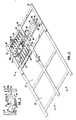
- a lead frame 10 constructed in accordance with the principles of the present invention includes a first axial section 12 and a second axial section 14 defined by a central axial bar 16 and two side bars 18 and 20.
- the first axial section 12 includes a plurality of individual lead frames 22, there usually being from about 12 to 24 individual frames 22 in a single lead frame strip 10.
- the individual lead frames 22 are generally conventional in construction and include a device paddle 26, a pair of paddle supports 28a and 28b, and a plurality of lead fingers 30.
- the paddle 26 and paddle supports 28 are connected between the central axial bar 16 and side bar 18, while the lead fingers 30 are supported by a tie bar 32 and transverse frame bars 34.
- paddle support 28b includes a lock slot 36.
- the second axial section 14 includes a plurality of ground plane plates 40 suspended on tabs 42a and 42b between the central axial bar 16 and side bar 20.
- Tab 42b terminates in a lock pin 43 which mates with lock slot 36 in paddle support 28b, as will be described in more detail hereinafter.
- the ground plane plates 40 are aligned with the individual lead frames 22 so that the connecting tab 42a of the plate is aligned with the paddle support 28a of the frame.
- Notches 44 are formed in the central axial bar 16 adjacent the connection to connecting tab 42a, as best observed in Fig. 2. The notches facilitate severing the paddle support 28a and connecting tab 42a from the bar 16 while leaving the tab and paddle support connected to each other.
- the ground plane plate 40 is generally rectangular having dimensions which exceed those of the paddle 26 of the lead frame 22. Usually, the length and width of the ground plane plate 40 will approximate the length and width of the final encapsulated package (as illustrated in Fig. 5).
- the ground plane plate 40 includes ground connection tabs 46 located generally at each corner of its rectangular surface. The connection tabs 46 will extend outside of the final encapsulated package and will be used to connect the ground plane to ground on the mounting substrate, typically a printed circuit board.
- Ground plane plate 40 also includes a plurality of bumps 50 formed in the surface. As illustrated in Figs. 1-2, the bumps 50 would extend downward away from the viewer so that, when the plate 40 is folded under the device paddle 26, the bumps 50 will project upward between adjacent lead fingers 30, as illustrated in Fig. 3. Conveniently, the bumps 50 will be formed by impressing the ground plane 40, but may also be formed by an additive process. Plate 40 also includes a plurality of holes 52 which allow the encapsulating material to penetrate the ground plane during transfer or injection molding.
- the lead frame 10 will be formed from conventional materials, typically copper, a copper alloy, Kovar®, or Alloy 42, by conventional pressing and stamping techniques, or by etching.
- the dimensions of the frame, number of lead fingers 30, and the like, are not critical. As illustrated, the lead frame is intended for a dual in-line package, but lead frames suitable for other packages, such as leaded quad packages, would also find use.
- the plastic semiconductor package of the present invention is assembled by first folding the ground plane plate 40 downward beneath the paddle 26 of the lead frame 22.
- the paddle will be folded without severing the connection of tab 42a to central axial bar 16 so that the lead frame strip 10 remains essentially intact.
- the lock pin 43 of connecting tab 42b is folded upward and inserted into lock slot 36 on paddle support 28b. Such folding results in the structure illustrated in Fig. 3, where the ground plate 40 is attached to the lead frame 22 by the folded connecting tab 42a.
- ground connection tabs 46 may be folded in a stepped configuration, as illustrated in Fig. 3.
- ground connection tabs 46 may be folded after molding is completed in order to simplify the molding operation.
- the paddle support 26 may be depressed downward, as illustrated in Fig. 4.
- a semiconductor die 60 is attached to the paddle 26 by conventional techniques, such as using a glass frit, a thermally-conducting epoxy, or a gold-silicon eutectic alloy.
- the bonding pads 62 on the die 60 are connected to the lead fingers 30 by conventional techniques, such as wire bonding or tape-automated bonding. See, Fig. 3A, where exemplary wire bonds 63 are illustrated.
- a ground ring 64 on the die 60 is connected to the bumps 50, either by wire bonding or tape-automated bonding (wire bonds 66 being illustrated).
- the bumps 50 lie between adjacent lead fingers 30 of the lead frame 22 so that the ground continuity continues between the lead fingers.
- the ground ring 64 By connecting the bumps 50 to the ground ring 64, the ground is further continued between the adjacent signal bonding connections, e.g., the wire bonds or tape-automated bonds.
- the ground ring 64 includes spikes 65 which project inward between adjacent bonding pads 62.
- the package may be completed by encapsulation using a conventional solid matrix encapsulant 70 (Fig. 5).
- a conventional solid matrix encapsulant 70 Conventional transfer or injection molding techniques are used to dispense the encapsulant around the lead frame 22 until the bonding wires 63 and 66, semiconductor die 50, and lead frame are fully covered and protected from the environment.
- the encapsulant is then cured, typically at an elevated temperature and controlled humidity, followed by the final trim and forming into a desired shape, as illustrated in Fig. 5.
- the connection tabs 42a and 42b may be trimmed from the package to complete the assembly process, as illustrated in Fig. 6.
Landscapes
- Structures Or Materials For Encapsulating Or Coating Semiconductor Devices Or Solid State Devices (AREA)
- Lead Frames For Integrated Circuits (AREA)
Applications Claiming Priority (2)
| Application Number | Priority Date | Filing Date | Title |
|---|---|---|---|
| US06/943,339 US4791473A (en) | 1986-12-17 | 1986-12-17 | Plastic package for high frequency semiconductor devices |
| US943339 | 1986-12-17 |
Publications (3)
| Publication Number | Publication Date |
|---|---|
| EP0272187A2 true EP0272187A2 (de) | 1988-06-22 |
| EP0272187A3 EP0272187A3 (en) | 1988-08-31 |
| EP0272187B1 EP0272187B1 (de) | 1992-10-28 |
Family
ID=25479483
Family Applications (1)
| Application Number | Title | Priority Date | Filing Date |
|---|---|---|---|
| EP87402883A Expired - Lifetime EP0272187B1 (de) | 1986-12-17 | 1987-12-17 | Plastikverpackung für Hochfrequenz-Halbleiteranordnungen |
Country Status (5)
| Country | Link |
|---|---|
| US (1) | US4791473A (de) |
| EP (1) | EP0272187B1 (de) |
| JP (1) | JPS63192260A (de) |
| KR (1) | KR960002497B1 (de) |
| DE (1) | DE3782406T2 (de) |
Cited By (3)
| Publication number | Priority date | Publication date | Assignee | Title |
|---|---|---|---|---|
| EP0560487A3 (en) * | 1992-02-07 | 1993-12-08 | Texas Instruments Inc | Semiconductor device having a lead frame |
| DE4318727A1 (de) * | 1992-06-05 | 1993-12-09 | Mitsubishi Electric Corp | Halbleitervorrichtung mit LOC-Struktur sowie dazugehöriges Herstellungsverfahren und dazugehöriger Zuführungsdraht-Rahmen |
| EP0595600A1 (de) * | 1992-10-26 | 1994-05-04 | Texas Instruments Incorporated | Umhüllung für Halbleiteranordnung |
Families Citing this family (52)
| Publication number | Priority date | Publication date | Assignee | Title |
|---|---|---|---|---|
| US4863806A (en) * | 1985-06-25 | 1989-09-05 | Hewlett-Packard Company | Optical isolator |
| US5148243A (en) * | 1985-06-25 | 1992-09-15 | Hewlett-Packard Company | Optical isolator with encapsulation |
| JP2522524B2 (ja) * | 1988-08-06 | 1996-08-07 | 株式会社東芝 | 半導体装置の製造方法 |
| US5099306A (en) * | 1988-11-21 | 1992-03-24 | Honeywell Inc. | Stacked tab leadframe assembly |
| US5183711A (en) * | 1988-12-13 | 1993-02-02 | Shinko Electric Industries Co., Ltd. | Automatic bonding tape used in semiconductor device |
| US4965654A (en) * | 1989-10-30 | 1990-10-23 | International Business Machines Corporation | Semiconductor package with ground plane |
| US5008615A (en) * | 1989-11-03 | 1991-04-16 | Motorola, Inc. | Means and method for testing integrated circuits attached to a leadframe |
| US5386141A (en) * | 1992-03-31 | 1995-01-31 | Vlsi Technology, Inc. | Leadframe having one or more power/ground planes without vias |
| US5376909A (en) * | 1992-05-29 | 1994-12-27 | Texas Instruments Incorporated | Device packaging |
| DE4345303C2 (de) * | 1992-06-05 | 2003-12-04 | Mitsubishi Electric Corp | Zuführungsdraht-Rahmen zur Verwendung bei der Herstellung einer Halbleitervorrichtung mit LOC-Struktur und Verfahren zur Herstellung einer Halbleitervorrichtung mit LOC-Struktur |
| US5457340A (en) * | 1992-12-07 | 1995-10-10 | Integrated Device Technology, Inc. | Leadframe with power and ground planes |
| US5442225A (en) * | 1993-08-13 | 1995-08-15 | Lsi Logic Corporation | Integrated circuit having interconnects with ringing suppressing elements |
| EP0668615A1 (de) * | 1994-02-18 | 1995-08-23 | Siemens Aktiengesellschaft | Kunststoff-SMD-Gehäuse für einen Halbleiterchip |
| US5485029A (en) * | 1994-06-30 | 1996-01-16 | International Business Machines Corporation | On-chip ground plane for semiconductor devices to reduce parasitic signal propagation |
| US5714792A (en) * | 1994-09-30 | 1998-02-03 | Motorola, Inc. | Semiconductor device having a reduced die support area and method for making the same |
| US5541565A (en) * | 1995-05-22 | 1996-07-30 | Trw Inc. | High frequency microelectronic circuit enclosure |
| US5969293A (en) * | 1997-07-18 | 1999-10-19 | National Semiconductor Corporation | Method and apparatus for doubling back single gauge lead frame |
| US6075283A (en) * | 1998-07-06 | 2000-06-13 | Micron Technology, Inc. | Downset lead frame for semiconductor packages |
| JP3444410B2 (ja) * | 2000-03-23 | 2003-09-08 | 株式会社三井ハイテック | リードフレームおよび半導体装置の製造方法 |
| US6246312B1 (en) | 2000-07-20 | 2001-06-12 | Cts Corporation | Ball grid array resistor terminator network |
| SG112799A1 (en) | 2000-10-09 | 2005-07-28 | St Assembly Test Services Ltd | Leaded semiconductor packages and method of trimming and singulating such packages |
| US6686258B2 (en) | 2000-11-02 | 2004-02-03 | St Assembly Test Services Ltd. | Method of trimming and singulating leaded semiconductor packages |
| US6777786B2 (en) * | 2001-03-12 | 2004-08-17 | Fairchild Semiconductor Corporation | Semiconductor device including stacked dies mounted on a leadframe |
| US7038305B1 (en) | 2003-07-15 | 2006-05-02 | Altera Corp. | Package for integrated circuit die |
| US7180186B2 (en) * | 2003-07-31 | 2007-02-20 | Cts Corporation | Ball grid array package |
| US6946733B2 (en) * | 2003-08-13 | 2005-09-20 | Cts Corporation | Ball grid array package having testing capability after mounting |
| US7196313B2 (en) * | 2004-04-02 | 2007-03-27 | Fairchild Semiconductor Corporation | Surface mount multi-channel optocoupler |
| CN101807533B (zh) * | 2005-06-30 | 2016-03-09 | 费查尔德半导体有限公司 | 半导体管芯封装及其制作方法 |
| US20090057852A1 (en) * | 2007-08-27 | 2009-03-05 | Madrid Ruben P | Thermally enhanced thin semiconductor package |
| US20070164428A1 (en) * | 2006-01-18 | 2007-07-19 | Alan Elbanhawy | High power module with open frame package |
| US7868432B2 (en) * | 2006-02-13 | 2011-01-11 | Fairchild Semiconductor Corporation | Multi-chip module for battery power control |
| US7768075B2 (en) | 2006-04-06 | 2010-08-03 | Fairchild Semiconductor Corporation | Semiconductor die packages using thin dies and metal substrates |
| US7656024B2 (en) | 2006-06-30 | 2010-02-02 | Fairchild Semiconductor Corporation | Chip module for complete power train |
| US7564124B2 (en) * | 2006-08-29 | 2009-07-21 | Fairchild Semiconductor Corporation | Semiconductor die package including stacked dice and heat sink structures |
| US7821116B2 (en) * | 2007-02-05 | 2010-10-26 | Fairchild Semiconductor Corporation | Semiconductor die package including leadframe with die attach pad with folded edge |
| US7659531B2 (en) * | 2007-04-13 | 2010-02-09 | Fairchild Semiconductor Corporation | Optical coupler package |
| US7902657B2 (en) * | 2007-08-28 | 2011-03-08 | Fairchild Semiconductor Corporation | Self locking and aligning clip structure for semiconductor die package |
| US20090057855A1 (en) * | 2007-08-30 | 2009-03-05 | Maria Clemens Quinones | Semiconductor die package including stand off structures |
| US20090140266A1 (en) * | 2007-11-30 | 2009-06-04 | Yong Liu | Package including oriented devices |
| US7589338B2 (en) * | 2007-11-30 | 2009-09-15 | Fairchild Semiconductor Corporation | Semiconductor die packages suitable for optoelectronic applications having clip attach structures for angled mounting of dice |
| KR20090062612A (ko) * | 2007-12-13 | 2009-06-17 | 페어차일드코리아반도체 주식회사 | 멀티 칩 패키지 |
| US20090166826A1 (en) * | 2007-12-27 | 2009-07-02 | Janducayan Omar A | Lead frame die attach paddles with sloped walls and backside grooves suitable for leadless packages |
| US8106406B2 (en) * | 2008-01-09 | 2012-01-31 | Fairchild Semiconductor Corporation | Die package including substrate with molded device |
| US20090194856A1 (en) * | 2008-02-06 | 2009-08-06 | Gomez Jocel P | Molded package assembly |
| KR101524545B1 (ko) * | 2008-02-28 | 2015-06-01 | 페어차일드코리아반도체 주식회사 | 전력 소자 패키지 및 그 제조 방법 |
| US8018054B2 (en) * | 2008-03-12 | 2011-09-13 | Fairchild Semiconductor Corporation | Semiconductor die package including multiple semiconductor dice |
| US7768108B2 (en) | 2008-03-12 | 2010-08-03 | Fairchild Semiconductor Corporation | Semiconductor die package including embedded flip chip |
| KR101519062B1 (ko) * | 2008-03-31 | 2015-05-11 | 페어차일드코리아반도체 주식회사 | 반도체 소자 패키지 |
| US20090278241A1 (en) * | 2008-05-08 | 2009-11-12 | Yong Liu | Semiconductor die package including die stacked on premolded substrate including die |
| US8193618B2 (en) | 2008-12-12 | 2012-06-05 | Fairchild Semiconductor Corporation | Semiconductor die package with clip interconnection |
| US7973393B2 (en) | 2009-02-04 | 2011-07-05 | Fairchild Semiconductor Corporation | Stacked micro optocouplers and methods of making the same |
| US8421204B2 (en) | 2011-05-18 | 2013-04-16 | Fairchild Semiconductor Corporation | Embedded semiconductor power modules and packages |
Family Cites Families (10)
| Publication number | Priority date | Publication date | Assignee | Title |
|---|---|---|---|---|
| JPS53132975A (en) * | 1977-04-26 | 1978-11-20 | Toshiba Corp | Semiconductor device |
| US4252864A (en) * | 1979-11-05 | 1981-02-24 | Amp Incorporated | Lead frame having integral terminal tabs |
| US4477827A (en) * | 1981-02-02 | 1984-10-16 | Northern Telecom Limited | Lead frame for leaded semiconductor chip carriers |
| US4551746A (en) * | 1982-10-05 | 1985-11-05 | Mayo Foundation | Leadless chip carrier apparatus providing an improved transmission line environment and improved heat dissipation |
| JPS5989438A (ja) * | 1982-11-15 | 1984-05-23 | Nippon Denso Co Ltd | 半導体装置 |
| IT1212711B (it) * | 1983-03-09 | 1989-11-30 | Ates Componenti Elettron | Dispositivo a semiconduttore aforma di scheda piana con contatti elettrici su ambedue le facce eprocedimento per la sua fabbricazione. |
| US4567545A (en) * | 1983-05-18 | 1986-01-28 | Mettler Rollin W Jun | Integrated circuit module and method of making same |
| US4680613A (en) * | 1983-12-01 | 1987-07-14 | Fairchild Semiconductor Corporation | Low impedance package for integrated circuit die |
| KR900001273B1 (ko) * | 1983-12-23 | 1990-03-05 | 후지쑤 가부시끼가이샤 | 반도체 집적회로 장치 |
| US4651415A (en) * | 1985-03-22 | 1987-03-24 | Diacon, Inc. | Leaded chip carrier |
-
1986
- 1986-12-17 US US06/943,339 patent/US4791473A/en not_active Expired - Lifetime
-
1987
- 1987-12-11 KR KR1019870014138A patent/KR960002497B1/ko not_active Expired - Fee Related
- 1987-12-17 EP EP87402883A patent/EP0272187B1/de not_active Expired - Lifetime
- 1987-12-17 JP JP62317608A patent/JPS63192260A/ja active Pending
- 1987-12-17 DE DE8787402883T patent/DE3782406T2/de not_active Expired - Fee Related
Cited By (10)
| Publication number | Priority date | Publication date | Assignee | Title |
|---|---|---|---|---|
| EP0560487A3 (en) * | 1992-02-07 | 1993-12-08 | Texas Instruments Inc | Semiconductor device having a lead frame |
| US5804871A (en) * | 1992-02-07 | 1998-09-08 | Texas Instruments Incorporated | Lead on chip semiconductor device having bus bars and crossing leads |
| DE4318727A1 (de) * | 1992-06-05 | 1993-12-09 | Mitsubishi Electric Corp | Halbleitervorrichtung mit LOC-Struktur sowie dazugehöriges Herstellungsverfahren und dazugehöriger Zuführungsdraht-Rahmen |
| US5535509A (en) * | 1992-06-05 | 1996-07-16 | Mitsubishi Denki Kabushiki Kaisha | Method of making a lead on chip (LOC) semiconductor device |
| US5724726A (en) * | 1992-06-05 | 1998-03-10 | Mitsubishi Denki Kabushiki Kaisha | Method of making leadframe for lead-on-chip (LOC) semiconductor device |
| DE4318727C2 (de) * | 1992-06-05 | 1998-03-12 | Mitsubishi Electric Corp | Verfahren zur Herstellung einer Halbleitervorrichtung mit LOC-Struktur sowie dazugehöriger Zuführungsdrahtrahmen |
| US5763829A (en) * | 1992-06-05 | 1998-06-09 | Mitsubishi Denki Kabushiki Kaisha | Leadframe including frame-cutting slit for lead-on-chip (LOC) semiconductor device and semiconductor device incorporating the leadframe |
| US5900582A (en) * | 1992-06-05 | 1999-05-04 | Mitsubishi Denki Kabushiki Kaisha | Lead frame including frame-cutting slit for lead-on-chip (LOC) semiconductor device and semiconductor device incorporating the lead frame |
| EP0595600A1 (de) * | 1992-10-26 | 1994-05-04 | Texas Instruments Incorporated | Umhüllung für Halbleiteranordnung |
| US5663597A (en) * | 1992-10-26 | 1997-09-02 | Texas Instruments Incorporated | RF device package for high frequency applications |
Also Published As
| Publication number | Publication date |
|---|---|
| US4791473A (en) | 1988-12-13 |
| KR960002497B1 (ko) | 1996-02-17 |
| KR880008440A (ko) | 1988-08-31 |
| JPS63192260A (ja) | 1988-08-09 |
| EP0272187A3 (en) | 1988-08-31 |
| EP0272187B1 (de) | 1992-10-28 |
| DE3782406D1 (de) | 1992-12-03 |
| DE3782406T2 (de) | 1993-05-06 |
Similar Documents
| Publication | Publication Date | Title |
|---|---|---|
| US4791473A (en) | Plastic package for high frequency semiconductor devices | |
| US6175149B1 (en) | Mounting multiple semiconductor dies in a package | |
| EP0228869B1 (de) | Verfahren zur Herstellung eines Gehäuses für ein elektronisches Bauelement | |
| US5332864A (en) | Integrated circuit package having an interposer | |
| US6297547B1 (en) | Mounting multiple semiconductor dies in a package | |
| US7102209B1 (en) | Substrate for use in semiconductor manufacturing and method of making same | |
| US9159588B2 (en) | Packaged leadless semiconductor device | |
| KR900002908B1 (ko) | 수지 봉지형 반도체 장치 | |
| US5444301A (en) | Semiconductor package and method for manufacturing the same | |
| US4974057A (en) | Semiconductor device package with circuit board and resin | |
| US5639694A (en) | Method for making single layer leadframe having groundplane capability | |
| US4891687A (en) | Multi-layer molded plastic IC package | |
| EP0774162B1 (de) | Herstellung zweiseitig drahtverbundener intergrierter schaltungschippackungen unter verwendung von offset-drahtverbindungen und trägerplatten mit hohlräumen | |
| US7432583B2 (en) | Leadless leadframe package substitute and stack package | |
| US7489021B2 (en) | Lead frame with included passive devices | |
| US20040150086A1 (en) | Semiconductor package having reduced thickness | |
| JPH06224246A (ja) | 半導体素子用高多端子化パッケージ | |
| JPH05343588A (ja) | 一部モールド型pcbチップキャリヤタイプパッケージ | |
| EP1994551A2 (de) | Verfahren zur herstellung eines qfn-pakets mit strom- und erdungsringen | |
| US6677665B2 (en) | Dual-die integrated circuit package | |
| KR19980032479A (ko) | 표면 설치 to-220 패키지 및 그의 제조 공정 | |
| US6791166B1 (en) | Stackable lead frame package using exposed internal lead traces | |
| US20070099344A1 (en) | Ultrathin leadframe BGA circuit package | |
| US6331452B1 (en) | Method of fabricating integrated circuit package with opening allowing access to die | |
| GB2199988A (en) | Multi-layer molded plastic ic package |
Legal Events
| Date | Code | Title | Description |
|---|---|---|---|
| PUAI | Public reference made under article 153(3) epc to a published international application that has entered the european phase |
Free format text: ORIGINAL CODE: 0009012 |
|
| AK | Designated contracting states |
Kind code of ref document: A2 Designated state(s): DE FR GB IT NL |
|
| PUAL | Search report despatched |
Free format text: ORIGINAL CODE: 0009013 |
|
| AK | Designated contracting states |
Kind code of ref document: A3 Designated state(s): DE FR GB IT NL |
|
| 17P | Request for examination filed |
Effective date: 19890222 |
|
| 17Q | First examination report despatched |
Effective date: 19910318 |
|
| GRAA | (expected) grant |
Free format text: ORIGINAL CODE: 0009210 |
|
| AK | Designated contracting states |
Kind code of ref document: B1 Designated state(s): DE FR GB IT NL |
|
| ITF | It: translation for a ep patent filed | ||
| REF | Corresponds to: |
Ref document number: 3782406 Country of ref document: DE Date of ref document: 19921203 |
|
| ET | Fr: translation filed | ||
| PLBE | No opposition filed within time limit |
Free format text: ORIGINAL CODE: 0009261 |
|
| STAA | Information on the status of an ep patent application or granted ep patent |
Free format text: STATUS: NO OPPOSITION FILED WITHIN TIME LIMIT |
|
| 26N | No opposition filed | ||
| PGFP | Annual fee paid to national office [announced via postgrant information from national office to epo] |
Ref country code: GB Payment date: 19941111 Year of fee payment: 8 |
|
| PGFP | Annual fee paid to national office [announced via postgrant information from national office to epo] |
Ref country code: FR Payment date: 19941209 Year of fee payment: 8 |
|
| PGFP | Annual fee paid to national office [announced via postgrant information from national office to epo] |
Ref country code: NL Payment date: 19941231 Year of fee payment: 8 |
|
| PG25 | Lapsed in a contracting state [announced via postgrant information from national office to epo] |
Ref country code: GB Effective date: 19951217 |
|
| PG25 | Lapsed in a contracting state [announced via postgrant information from national office to epo] |
Ref country code: NL Effective date: 19960701 |
|
| GBPC | Gb: european patent ceased through non-payment of renewal fee |
Effective date: 19951217 |
|
| PG25 | Lapsed in a contracting state [announced via postgrant information from national office to epo] |
Ref country code: FR Effective date: 19960830 |
|
| NLV4 | Nl: lapsed or anulled due to non-payment of the annual fee |
Effective date: 19960701 |
|
| REG | Reference to a national code |
Ref country code: FR Ref legal event code: ST |
|
| PG25 | Lapsed in a contracting state [announced via postgrant information from national office to epo] |
Ref country code: IT Free format text: LAPSE BECAUSE OF NON-PAYMENT OF DUE FEES;WARNING: LAPSES OF ITALIAN PATENTS WITH EFFECTIVE DATE BEFORE 2007 MAY HAVE OCCURRED AT ANY TIME BEFORE 2007. THE CORRECT EFFECTIVE DATE MAY BE DIFFERENT FROM THE ONE RECORDED. Effective date: 20051217 |
|
| PGFP | Annual fee paid to national office [announced via postgrant information from national office to epo] |
Ref country code: DE Payment date: 20060131 Year of fee payment: 19 |
|
| PG25 | Lapsed in a contracting state [announced via postgrant information from national office to epo] |
Ref country code: DE Free format text: LAPSE BECAUSE OF NON-PAYMENT OF DUE FEES Effective date: 20070703 |