EP0272531A1 - Flächenschleifmaschine - Google Patents
Flächenschleifmaschine Download PDFInfo
- Publication number
- EP0272531A1 EP0272531A1 EP87118077A EP87118077A EP0272531A1 EP 0272531 A1 EP0272531 A1 EP 0272531A1 EP 87118077 A EP87118077 A EP 87118077A EP 87118077 A EP87118077 A EP 87118077A EP 0272531 A1 EP0272531 A1 EP 0272531A1
- Authority
- EP
- European Patent Office
- Prior art keywords
- wheel
- wafer
- grinding machine
- surface grinding
- diamond
- Prior art date
- Legal status (The legal status is an assumption and is not a legal conclusion. Google has not performed a legal analysis and makes no representation as to the accuracy of the status listed.)
- Granted
Links
- 238000000227 grinding Methods 0.000 title claims abstract description 94
- 229910003460 diamond Inorganic materials 0.000 claims abstract description 59
- 239000010432 diamond Substances 0.000 claims abstract description 59
- 239000006061 abrasive grain Substances 0.000 claims abstract description 39
- 150000001875 compounds Chemical class 0.000 claims abstract description 36
- 239000004065 semiconductor Substances 0.000 claims abstract description 36
- 230000007423 decrease Effects 0.000 claims abstract description 8
- 238000012545 processing Methods 0.000 claims description 31
- 239000000463 material Substances 0.000 claims description 23
- 239000000945 filler Substances 0.000 claims description 17
- 239000011347 resin Substances 0.000 claims description 16
- 229920005989 resin Polymers 0.000 claims description 16
- VTYYLEPIZMXCLO-UHFFFAOYSA-L Calcium carbonate Chemical group [Ca+2].[O-]C([O-])=O VTYYLEPIZMXCLO-UHFFFAOYSA-L 0.000 claims description 8
- 229910000019 calcium carbonate Inorganic materials 0.000 claims description 4
- 239000005011 phenolic resin Substances 0.000 claims description 3
- KXGFMDJXCMQABM-UHFFFAOYSA-N 2-methoxy-6-methylphenol Chemical group [CH]OC1=CC=CC([CH])=C1O KXGFMDJXCMQABM-UHFFFAOYSA-N 0.000 claims description 2
- 229920001568 phenolic resin Polymers 0.000 claims description 2
- 239000011230 binding agent Substances 0.000 claims 1
- 235000012431 wafers Nutrition 0.000 description 111
- 238000000034 method Methods 0.000 description 19
- XUIMIQQOPSSXEZ-UHFFFAOYSA-N Silicon Chemical compound [Si] XUIMIQQOPSSXEZ-UHFFFAOYSA-N 0.000 description 8
- 229910052710 silicon Inorganic materials 0.000 description 8
- 239000010703 silicon Substances 0.000 description 8
- 229910001218 Gallium arsenide Inorganic materials 0.000 description 7
- 239000007788 liquid Substances 0.000 description 7
- 239000013078 crystal Substances 0.000 description 5
- 229920001971 elastomer Polymers 0.000 description 5
- 238000002474 experimental method Methods 0.000 description 5
- 239000002699 waste material Substances 0.000 description 5
- PNEYBMLMFCGWSK-UHFFFAOYSA-N aluminium oxide Inorganic materials [O-2].[O-2].[O-2].[Al+3].[Al+3] PNEYBMLMFCGWSK-UHFFFAOYSA-N 0.000 description 4
- 239000007787 solid Substances 0.000 description 4
- RYGMFSIKBFXOCR-UHFFFAOYSA-N Copper Chemical compound [Cu] RYGMFSIKBFXOCR-UHFFFAOYSA-N 0.000 description 3
- 238000003776 cleavage reaction Methods 0.000 description 3
- 238000010276 construction Methods 0.000 description 3
- 238000010586 diagram Methods 0.000 description 3
- 230000020169 heat generation Effects 0.000 description 3
- 230000002093 peripheral effect Effects 0.000 description 3
- 238000005498 polishing Methods 0.000 description 3
- 230000005855 radiation Effects 0.000 description 3
- 230000007017 scission Effects 0.000 description 3
- HBMJWWWQQXIZIP-UHFFFAOYSA-N silicon carbide Chemical compound [Si+]#[C-] HBMJWWWQQXIZIP-UHFFFAOYSA-N 0.000 description 3
- 229910010271 silicon carbide Inorganic materials 0.000 description 3
- 230000003746 surface roughness Effects 0.000 description 3
- 238000005452 bending Methods 0.000 description 2
- 238000005530 etching Methods 0.000 description 2
- 229910052751 metal Inorganic materials 0.000 description 2
- 239000002184 metal Substances 0.000 description 2
- 230000000704 physical effect Effects 0.000 description 2
- 229910005542 GaSb Inorganic materials 0.000 description 1
- 239000003082 abrasive agent Substances 0.000 description 1
- 239000010953 base metal Substances 0.000 description 1
- 230000015572 biosynthetic process Effects 0.000 description 1
- 239000000919 ceramic Substances 0.000 description 1
- 229910052593 corundum Inorganic materials 0.000 description 1
- 238000005520 cutting process Methods 0.000 description 1
- 230000003247 decreasing effect Effects 0.000 description 1
- WPYVAWXEWQSOGY-UHFFFAOYSA-N indium antimonide Chemical compound [Sb]#[In] WPYVAWXEWQSOGY-UHFFFAOYSA-N 0.000 description 1
- 230000010354 integration Effects 0.000 description 1
- 238000005468 ion implantation Methods 0.000 description 1
- 238000010030 laminating Methods 0.000 description 1
- 238000004519 manufacturing process Methods 0.000 description 1
- 229920001721 polyimide Polymers 0.000 description 1
- 239000009719 polyimide resin Substances 0.000 description 1
- 238000012805 post-processing Methods 0.000 description 1
- 239000000843 powder Substances 0.000 description 1
- 239000007779 soft material Substances 0.000 description 1
- 239000000758 substrate Substances 0.000 description 1
- 238000007740 vapor deposition Methods 0.000 description 1
- 238000005406 washing Methods 0.000 description 1
- XLYOFNOQVPJJNP-UHFFFAOYSA-N water Substances O XLYOFNOQVPJJNP-UHFFFAOYSA-N 0.000 description 1
- 229910001845 yogo sapphire Inorganic materials 0.000 description 1
Images

Classifications
-
- B—PERFORMING OPERATIONS; TRANSPORTING
- B24—GRINDING; POLISHING
- B24D—TOOLS FOR GRINDING, BUFFING OR SHARPENING
- B24D3/00—Physical features of abrasive bodies, or sheets, e.g. abrasive surfaces of special nature; Abrasive bodies or sheets characterised by their constituents
- B24D3/02—Physical features of abrasive bodies, or sheets, e.g. abrasive surfaces of special nature; Abrasive bodies or sheets characterised by their constituents the constituent being used as bonding agent
- B24D3/20—Physical features of abrasive bodies, or sheets, e.g. abrasive surfaces of special nature; Abrasive bodies or sheets characterised by their constituents the constituent being used as bonding agent and being essentially organic
- B24D3/28—Resins or natural or synthetic macromolecular compounds
-
- B—PERFORMING OPERATIONS; TRANSPORTING
- B24—GRINDING; POLISHING
- B24B—MACHINES, DEVICES, OR PROCESSES FOR GRINDING OR POLISHING; DRESSING OR CONDITIONING OF ABRADING SURFACES; FEEDING OF GRINDING, POLISHING, OR LAPPING AGENTS
- B24B7/00—Machines or devices designed for grinding plane surfaces on work, including polishing plane glass surfaces; Accessories therefor
- B24B7/10—Single-purpose machines or devices
- B24B7/16—Single-purpose machines or devices for grinding end-faces, e.g. of gauges, rollers, nuts, piston rings
-
- B—PERFORMING OPERATIONS; TRANSPORTING
- B24—GRINDING; POLISHING
- B24B—MACHINES, DEVICES, OR PROCESSES FOR GRINDING OR POLISHING; DRESSING OR CONDITIONING OF ABRADING SURFACES; FEEDING OF GRINDING, POLISHING, OR LAPPING AGENTS
- B24B49/00—Measuring or gauging equipment for controlling the feed movement of the grinding tool or work; Arrangements of indicating or measuring equipment, e.g. for indicating the start of the grinding operation
- B24B49/16—Measuring or gauging equipment for controlling the feed movement of the grinding tool or work; Arrangements of indicating or measuring equipment, e.g. for indicating the start of the grinding operation taking regard of the load
Definitions
- the present invention relates to a surface grinding machine for grinding the back surface of a wafer of a single crystal III-V group compound seimiconductor on which elements have been fabricated.
- III-V group compound semiconductors include GaAs. InSb, InP, GaP, GaSb, etc. These compound semiconductors have a common disadvantage in that they are soft and fragile compared with silicon.
- a single crystal of a compound semiconductor is prepared by the Liquid Encapsulated Czochralski (LEC) or Horizontal Bridgman (HB) method.
- LEC Liquid Encapsulated Czochralski
- HB Horizontal Bridgman
- the single crystal compound semiconductor is ground into a columnar shape with the orientation flat (OF) or IF.
- the columnar single crystal ingot is cut into thin discs (or square plates) called an as-cut-wafer.
- the as-cut-wafers are subjected to both or one side lapping, and both sides or one side of each is subjected to mirror polishing.
- the wafer is subjected to etching several times to remove the layer changed in property by working, and often subjected to beveling to round the peripheral edge.
- the product thus obtained is called a mirror wafer.
- the present invention is not concerned with grinding in the process of making the mirror wafer from the as-cut-wafer.
- the elements are fabricated on the mirror wafer by repeating wafer processes.
- the elements may be light emitting elements, integrated circuits of high-speed logic elements, light receiving elements, or elements for detecting infrared rays etc.
- varieties of water process such as epitaxial growth, ion implantation, etching, vapor deposition, or insulating film formation, are used.
- the present invention is intended for a wafer on which elements have been fabricated.
- the wafer with elements is roughly 620 ⁇ m ⁇ 700 ⁇ m thick for a 3 inch diameter since the thickness of the mirror wafer is just about that size.
- the thickness of a layer slightly changes because of epitaxial growth or the like by several ⁇ m to the utmost so that the thickness of the wafer almost equals to that of the mirror wafer.
- the wafer is a little thick since the mechanical strength is required when elements are fabricated. If the wafer is thinner than the above value, the handling of the wafer is difficult.
- the wafer In case that a semiconductor element is fabricated, the wafer is only used as a substrate and its surface of only several ⁇ m thick is necessary for the fabrication. The other part of the wafer is required to simply impart it mechanical strength.
- the back thereof is ground to reduce its thickness in case that a great deal of thermal generation occurs. Since the thermal conductivity of silicon is excellent, it is sufficient to reduce the thickness to about 400 ⁇ m.
- lapping is employed to grind the back thereof.
- the lapping employed in this stage is different in purpose from that employed in the process of making the mirror wafer from the as-cut-wafer.
- the technique is similar to each other.
- the surface of the wafer is secured to a suitable pressure disc.
- By turning the pressure disc and contacting the disc to a platen while supplying an abrasive the back of the wafer is lapped by the rotation of the platen and the pressure disc.
- the abrasive contains a large amount of abrasive grains. The back of the wafer physically contacts the abrasive grains and is shaved.
- lapping is usable to make the wafer 400 ⁇ m thick, it is wet processing and therefore not necessarily a good method. That is, the processing time including pre- and after-processing is lengthy. As the abrasive grains are used, they may be embedded in the surface of the wafer on which elements are fabricated and thus must be washed off. The layer changed in property by lapping is large. Also, there is a problem of dealing with a large amount of waste liquid. Moreover, automation cannot be attained due to the batch processing. As set forth above, there are a number of disadvantages in the lapping method for shaving the back of the wafer on which elements are not fabricated.
- the present inventors have succeeded in realizing a method of grinding the back of the Si wafer by a diamond wheel.
- the method uses a surface grinding machine as disclosed in Japanese Unexamined Published Application No. 95866/86 (laid open on May 14, 1986).
- Such grinding the back of the wafer by means of the diamond wheel is simply called backing grinding.
- the back grinding is being used instead of lapping in order to reduce the thickness of the Si wafer.
- lapping is mainly used at present, back grinding seems to be mainly used in the future.
- the thermal conductivity of the III-V group compound is lower than that of the Si wafer and, because the former compound is operated at high speed, it generates a great deal of heat. For that reason, the III-V group compound must be made as thin as up to 200 ⁇ m, whereas it is only necessary to make the Si wafer as thin as up to 400 ⁇ m. The III-V group compound is more disadvantageous as compared with the Si wafer.
- the compound semiconductor wafer is likely to be broken when physically contacting with the wheel. It is often broken because it is to be shaved as thin as about half of that of the Si wafer notwithstanding its fragility compared with the si wafer.
- the surface thereof will be torn off along its cleavage plane. In other words, there are produced a number of cavities in the surface thereof. this is because the abrasive grains fixed to the wheel scrape the soft portion of the surface thereof locally.
- the back of the wafer does not become a mirror surface. If the back thereof is not a mirror surface, the chip will not smoothly contact with the package when the chip is die-bonded to the package and this causes the thermal resistance to inconveniently increase.
- the present inventors have made experiments in search of a method of grinding the back of a compound semiconductor wafer by means of a diamond wheel.
- the filler which contributes to binding but not to grinding, consists of solid grains.
- As the filler calcium carbonate, alumina, silicon carbide, copper powder or the like is usable. Although they are solid, they will not function as abrasive grains and only occupy a space. Therefore, they are solid powder having the diameter smaller than that of the diamond abrasive grain.
- the bond material is used to uniformly distribute the diamond abrasive grains and the filler to combine them so that the combination may have a fixed shape.
- a resin bond, a metal bond or a vitrified bond is usable.
- rubber may be used as the bond material to make a rubber wheel.
- the present invention is concerned with the resin bond wheel.
- Resin is used as a bond material.
- phenol resin is mainly used.
- Polyimide resin may also be usable.
- Diamond abrasive grains are most important among three components of the wheel since they mainly carry out the grinding operation.
- the diamond abrasive grains are defined by two parameters: i.e., grain size and concentration.
- the size of abrasive grains of a usable diamond wheel ranges from #2,000 (6 ⁇ m) to #4,000 (2.5 ⁇ m). Grain size of #3,000 corresponds to an average diameter of about 3 ⁇ m.
- the wheel is formed into a ring shape and secured to the circumferential end face of a wheel head with a U-shaped cross section. It is called a cup-shaped wheel because it looks like a bowl.
- the purpose is to grind the back of the compound semiconductor into a mirror surface. Further, it is important to grind the back of the semiconductor up to a thickness of about 200 ⁇ m without breaking the wafer or tearing the back thereof.
- the present inventors ground a number of compound semiconductors and made experiments under many conditions. As a result, the inventors found that although the conditions E-I should be within a suitable range, the range are not perculiar to the compound semiconductor wafer. On the other hand, the physical properties A-D of the wheel were seen to be closely related to polishing the wafer into a mirror surface without cleaving it. However, the optimum grinding conditions cannot be defined even through one of the conditions A-D is determined. Some of conditions A-D are related to one another.
- the Young's modulus is determined by the conditions A-D.
- An optimum wheel may be given by defining the Young's modulus without defining any one of A-D.
- the present inventors have come to know this fact through a number of experiments.
- lapping is the technique used to make the back of the compound semiconductor wafer into a thin layer. Although not only troublesome of handling but also difficulty in dealing with waste liquid has posed a serious problem, lapping may be said to be the best method for a wafer.
- a grinding wheel containing a bond material made of soft material In order to make J smaller, it is preferred to use a grinding wheel containing a bond material made of soft material.
- a rubber wheel containing a bond material of rubber, whose Young's modulus J is small is preferred.
- J is smaller than that value, the friction between the resin and the wafer will mainly occur and the strong frictional force caused thereby will damage the wafer. If J is greater than that value, the wafer will not be polished into a mirror surface.
- the grinding resistance means a resistant force received by the wheel due to the contact with the wafer.
- the grinding resistance is given in the form of torque because the wheel is rotary body.
- the grinding resistance is the frictional force applied to the wafer in some aspect. If the grinding resistance is 0, grinding will be impossible. If the grinding resistance is great, the great frictional force applied to the wafer will damage the wafer.
- the grinding resistance should preferably be constant. However, the grinding resistance R fluctuates in accordance with the cutting property of the grinding wheel and the condition under which cut chips are discharged.
- the fluctuation of the grinding resistance R appears in the form of torque applied to the axis of the wheel. This is the torque to suppress the rotation of a motor. If the resistance R increases, the number of rotations ⁇ will decrease, whereas the current value I of the motor will increase.
- the relation between the reverse torque and the number of rotations ⁇ and the current value I is fixed, because the motor for rotating the wheel is a DC motor.
- the current value I fluctuates because the voltage is made constant in that case. If R decreases, ⁇ will increase, whereas I will decrease.
- a chuck table drive motor 4 is used to turn the chuck tables 2.
- a grinding wheel head 5 is a member vertically movable, and a grinding wheel shaft 7 and a cup-shaped diamond wheel 6 are fitted to the lower end thereof, whereas a motor 8 for driving the wheel shaft 7 is fitted to the upper portion thereof.
- the wheel shaft 7 is driven and rotated by the motor 8.
- the cup-shaped diamond wheel 6 is simultaneously turned and, when the wheel head is lowered, the wafer 1 is ground by the cup-shaped diamond wheel 6.
- the cup-shaped diamond wheel 6 is a grinding wheel including a base metal and an abrasive grain layer 13 and it is so called because it looks like a cup.
- the wheel head 5 is guided along a vertical line by a vertical slide 11.
- a screw dowel 14 is fixed to the back face of the wheel head 5.
- a rotatable screw 9 is screwed into a female screw hole of the screw dowel 14.
- the slide 11 is a rail-like member fitted to a part of a fixed member 12.
- the screw 9 is rotated by a servomotor 10 fixed to a bracket 16 installed at the upper end of the fixed member 12.
- the servomotor 10 is rotatable clockwise and counterclockwise and its speed can freely be adjusted.
- the screw 9 is rotated by the servomotor to move the wheel head 5, vertically. By the down movement of the wheel head, the wafer face is ground little by little.
- the speed at which the wheel head moves down during grinding is equal to a feed speed ⁇ .
- a plurality of wheel heads, cup-shaped diamond wheels, wheel shafts, servomotors, etc. may be provided so that a plurality of wafers can be simultaneously processed.
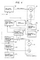
- Fig. 4 shows a block diagram showing circuits for keeping the grinding resistance constant.
- the construction itself of each of circuits is well known so that a detailed description of each circuit is omitted.
- the current I of the motor 8 for driving the wheel shaft is detected by a main shaft current value measuring device 32 and is applied to the main shaft motor current value analysis circuit 30, which also receives a predetermined current value from a main shaft current setting device 34.
- the rotation number ⁇ of the wheel shaft 7 is detected by the main shaft rotation speed analysis circuit 40, to which a predetermined rotation number is also applied from a main shaft rotation number setting device 44.
- a feed comparator 56 receives a predetermined grinding speed from a standard grinding setting device 54 and receives a feed speed from the servomotor 10.
- the output of each of circuits 30, 40 and 56 is applied to the feed speed control circuit 50, which compares a normal grinding resistance R0 with a calculated present grinding resistance R to adjust the grinding speed ⁇ so as to bring R close to R0.
- the feed speed is set to fluctuate within 0 - 2 ⁇ m/min.
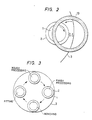
- the center 0 of the abrasive grain layer 13 is shifted from the center 0 ⁇ of the wheel shaft.
- Such eccentric movement has been described in the aforesaid Japanese Patent Unexamined Published Application No. 95866/86.
- the diamond wheel of the surface grinding machine according to the present invention has a Young's modulus of (10 - 15) ⁇ 104 kgf/cm2.
- the usable abrasive diamond grain size ranges from #2,000 (6 ⁇ m) to #4,000 (2.5 ⁇ m). This grain size is one normally used for surface grinding.
- the concentration is any one between 50 - 200.
- the inner diameter F, outer diameter G and thickness E of the wheel are optional.
- a resin bonded diamond wheel is used in the present invention, its bond material is resin.
- the filler is alumina, calcium carbonate, silicon carbide, copper powder or the like.
- the abrasive grains are diamond.
- the Young's modulus becomes greater.
- the Young's modulus becomes smaller.
- the filler contributes to increasing rigidity but provides no grinding action. For this reason, it must be composed of solid fine grains with the grain size smaller than diamond abrasive grain size.
- the condition of the Young's modulus according to the present invention is intended for finish processing.
- the whole process may be carried out under the same condition without dividing it into two step.
- the GaAs wafer was 3 inches in diameter.
- the peripheral speed of the grinding wheel was set at 2,200 m/min.
- the feed speed was set at 1 ⁇ m/min.
- the thickness of the wafer thus ground was 200 ⁇ m.
- the volume ratios of the resins, the fillers and abrasive diamond grains of the diamond wheels A - F were as follows:
- Phenolic resin was employed as the resin. Calcium carbonate was mainly used as the filler. However, the results were the same when alumina, silicon carbide or copper powder were used.
- the wheel A When the wheel A was used, a mirror surface at the surface roughness of 0.1 ⁇ Rmax was obtained. However, the wafers were frequently broken. Accordingly, the wheel A was not suitable.
- the wheels B, C, D and E could be used to grind the wafers up to 200 ⁇ m without breakage and to polish into a mirror surface of the surface roughness 0.1 ⁇ Rmax.
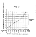
- Fig. 5 is a graph showing the measured values of the Young's moduli of the wheels A- F.
- the horizontal axis represents the volume ratios (%) of the resins and the fillers, whereas the vertical axis represents the Young's modulus (kgf/cm2).
- the wafer was often broken when the wheel A was used, and the wafer was not polished into a mirror surface when the wheel F was used. That is, the Young's modulus smaller than 10 ⁇ 104 kgf/cm2 or greater than 15 ⁇ 104 kgf/cm2 was unsuitable.
- the diamond filling ratio was set at 100 (25vol%).
- the diamond filling ratio may be changed. In this case, the vol% of the resin and the filler does not become 75% in total.
- the Young's modulus should be (10 -15) ⁇ 104 kgf/cm2.
Landscapes
- Engineering & Computer Science (AREA)
- Mechanical Engineering (AREA)
- Mechanical Treatment Of Semiconductor (AREA)
- Polishing Bodies And Polishing Tools (AREA)
Applications Claiming Priority (4)
| Application Number | Priority Date | Filing Date | Title |
|---|---|---|---|
| JP61291901A JPH0632905B2 (ja) | 1986-12-08 | 1986-12-08 | ▲iii▼―v族化合物半導体ウエハ薄層化処理方法 |
| JP291901/86 | 1986-12-08 | ||
| JP294351/86 | 1986-12-10 | ||
| JP61294351A JPS63150158A (ja) | 1986-12-10 | 1986-12-10 | 端面研削盤切込み装置 |
Publications (2)
| Publication Number | Publication Date |
|---|---|
| EP0272531A1 true EP0272531A1 (de) | 1988-06-29 |
| EP0272531B1 EP0272531B1 (de) | 1991-07-31 |
Family
ID=26558752
Family Applications (1)
| Application Number | Title | Priority Date | Filing Date |
|---|---|---|---|
| EP87118077A Expired - Lifetime EP0272531B1 (de) | 1986-12-08 | 1987-12-07 | Flächenschleifmaschine |
Country Status (5)
| Country | Link |
|---|---|
| US (1) | US5035087A (de) |
| EP (1) | EP0272531B1 (de) |
| KR (1) | KR960015957B1 (de) |
| CA (1) | CA1307116C (de) |
| DE (1) | DE3771857D1 (de) |
Cited By (27)
| Publication number | Priority date | Publication date | Assignee | Title |
|---|---|---|---|---|
| EP0387259A4 (en) * | 1988-08-19 | 1991-07-24 | James W. Kinner | Flywheel resurfacing method and apparatus |
| GB2275130A (en) * | 1992-05-26 | 1994-08-17 | Toshiba Kk | Polishing apparatus and method for planarizing layer on a semiconductor wafer |
| US5400548A (en) * | 1992-07-23 | 1995-03-28 | Wacker-Chemitronic Gesellschaft Fur Elektronik-Grundstoffe Mbh | Process for manufacturing semiconductor wafers having deformation ground in a defined way |
| US5445996A (en) * | 1992-05-26 | 1995-08-29 | Kabushiki Kaisha Toshiba | Method for planarizing a semiconductor device having a amorphous layer |
| GB2324750A (en) * | 1997-04-28 | 1998-11-04 | Nec Corp | Automatic wafer polishing apparatus |
| DE19833257C1 (de) * | 1998-07-23 | 1999-09-30 | Wacker Siltronic Halbleitermat | Verfahren zur Herstellung einer Halbleiterscheibe |
| EP0955126A3 (de) * | 1998-05-06 | 2000-04-05 | Shin-Etsu Handotai Co., Ltd. | Verfahren und Vorrichtung zum Schleifen der Oberfläche einer Halbleiterscheibe |
| US6340326B1 (en) | 2000-01-28 | 2002-01-22 | Lam Research Corporation | System and method for controlled polishing and planarization of semiconductor wafers |
| EP0874390A4 (de) * | 1995-09-13 | 2002-02-06 | Hitachi Ltd | Schleifverfahren und vorrichtung |
| DE10064081C2 (de) * | 2000-12-21 | 2002-06-06 | Wacker Siltronic Halbleitermat | Verfahren zur Herstellung einer Halbleiterscheibe |
| US6443815B1 (en) | 2000-09-22 | 2002-09-03 | Lam Research Corporation | Apparatus and methods for controlling pad conditioning head tilt for chemical mechanical polishing |
| US6471566B1 (en) | 2000-09-18 | 2002-10-29 | Lam Research Corporation | Sacrificial retaining ring CMP system and methods for implementing the same |
| US6478977B1 (en) | 1995-09-13 | 2002-11-12 | Hitachi, Ltd. | Polishing method and apparatus |
| EP1308243A1 (de) * | 1995-09-13 | 2003-05-07 | Hitachi, Ltd. | Polierverfahren |
| US6640155B2 (en) | 2000-08-22 | 2003-10-28 | Lam Research Corporation | Chemical mechanical polishing apparatus and methods with central control of polishing pressure applied by polishing head |
| US6652357B1 (en) | 2000-09-22 | 2003-11-25 | Lam Research Corporation | Methods for controlling retaining ring and wafer head tilt for chemical mechanical polishing |
| US6705930B2 (en) | 2000-01-28 | 2004-03-16 | Lam Research Corporation | System and method for polishing and planarizing semiconductor wafers using reduced surface area polishing pads and variable partial pad-wafer overlapping techniques |
| DE10009656B4 (de) * | 2000-02-24 | 2005-12-08 | Siltronic Ag | Verfahren zur Herstellung einer Halbleiterscheibe |
| CN1303654C (zh) * | 1995-09-13 | 2007-03-07 | 株式会社日立制作所 | 抛光方法和设备 |
| US7481695B2 (en) | 2000-08-22 | 2009-01-27 | Lam Research Corporation | Polishing apparatus and methods having high processing workload for controlling polishing pressure applied by polishing head |
| US7579261B2 (en) | 2005-09-22 | 2009-08-25 | Siltronic Ag | Epitaxially coated silicon wafer and method for producing epitaxially coated silicon wafers |
| DE102008026784A1 (de) | 2008-06-04 | 2009-12-10 | Siltronic Ag | Epitaxierte Siliciumscheibe mit <110>-Kristallorientierung und Verfahren zu ihrer Herstellung |
| US7659207B2 (en) | 2005-09-22 | 2010-02-09 | Siltronic Ag | Epitaxially coated silicon wafer and method for producing epitaxially coated silicon wafer |
| DE102009004557A1 (de) | 2009-01-14 | 2010-07-15 | Siltronic Ag | Epitaxierte Siliciumscheibe und Verfahren zur Herstellung von epitaxierten Siliciumscheiben |
| DE102009010556A1 (de) | 2009-02-25 | 2010-09-02 | Siltronic Ag | Verfahren zur Herstellung von epitaxierten Siliciumscheiben |
| DE102009025243A1 (de) | 2009-06-17 | 2010-12-30 | Siltronic Ag | Verfahren zur Herstellung und Verfahren zur Bearbeitung einer Halbleiterscheibe |
| US7922813B2 (en) | 2005-09-22 | 2011-04-12 | Siltronic Ag | Epitaxially coated silicon wafer and method for producing epitaxially coated silicon wafers |
Families Citing this family (60)
| Publication number | Priority date | Publication date | Assignee | Title |
|---|---|---|---|---|
| WO1990009870A1 (en) * | 1989-02-23 | 1990-09-07 | Supfina Maschinenfabrik Hentzen Gmbh & Co. Kg | Method and apparatus for fine working or microfinishing |
| JP2610703B2 (ja) * | 1990-09-05 | 1997-05-14 | 住友電気工業株式会社 | 半導体素子の製造方法 |
| DE4134110A1 (de) * | 1991-10-15 | 1993-04-22 | Wacker Chemitronic | Verfahren zum rotationssaegen sproedharter werkstoffe, insbesondere solcher mit durchmessern ueber 200 mm in duenne scheiben vermittels innenlochsaege und vorrichtung zur durchfuehrung des verfahrens |
| US5538460A (en) * | 1992-01-16 | 1996-07-23 | System Seiko Co., Ltd. | Apparatus for grinding hard disk substrates |
| DE4392793T1 (de) * | 1992-06-15 | 1997-07-31 | Speedfam Corp | Verfahren und Vorrichtung zum Polieren von Wafern |
| US5329732A (en) * | 1992-06-15 | 1994-07-19 | Speedfam Corporation | Wafer polishing method and apparatus |
| US5314107A (en) * | 1992-12-31 | 1994-05-24 | Motorola, Inc. | Automated method for joining wafers |
| US5441437A (en) * | 1993-02-18 | 1995-08-15 | Hulstedt; Bryan A. | Compliant constant-force follower device for surface finishing tool |
| JP3363587B2 (ja) * | 1993-07-13 | 2003-01-08 | キヤノン株式会社 | 脆性材料の加工方法及びその装置 |
| NO179238C (no) * | 1994-06-15 | 1996-09-04 | Norsk Hydro As | Utstyr for tynnsliping av materialpröver |
| JP3055401B2 (ja) * | 1994-08-29 | 2000-06-26 | 信越半導体株式会社 | ワークの平面研削方法及び装置 |
| JPH0947947A (ja) * | 1994-08-30 | 1997-02-18 | Seiko Seiki Co Ltd | 研削装置、並びに研削方法、並びに半導体装置及び半導体基板の製造方法 |
| US5665656A (en) * | 1995-05-17 | 1997-09-09 | National Semiconductor Corporation | Method and apparatus for polishing a semiconductor substrate wafer |
| US5655956A (en) * | 1995-05-23 | 1997-08-12 | University Of Illinois At Urbana-Champaign | Rotary ultrasonic grinding apparatus and process |
| EP1297927A3 (de) * | 1995-09-13 | 2003-04-09 | Hitachi, Ltd. | Poliervorrichtung |
| US5954570A (en) * | 1996-05-31 | 1999-09-21 | Kabushiki Kaisha Toshiba | Conditioner for a polishing tool |
| US6425812B1 (en) | 1997-04-08 | 2002-07-30 | Lam Research Corporation | Polishing head for chemical mechanical polishing using linear planarization technology |
| US6244946B1 (en) | 1997-04-08 | 2001-06-12 | Lam Research Corporation | Polishing head with removable subcarrier |
| TW377467B (en) * | 1997-04-22 | 1999-12-21 | Sony Corp | Polishing system, polishing method, polishing pad, and method of forming polishing pad |
| JPH10296610A (ja) * | 1997-04-28 | 1998-11-10 | Sony Corp | 研磨方法 |
| CN1272222A (zh) * | 1997-08-21 | 2000-11-01 | Memc电子材料有限公司 | 处理半导体晶片的方法 |
| US5827111A (en) * | 1997-12-15 | 1998-10-27 | Micron Technology, Inc. | Method and apparatus for grinding wafers |
| US5827112A (en) * | 1997-12-15 | 1998-10-27 | Micron Technology, Inc. | Method and apparatus for grinding wafers |
| US6517427B1 (en) * | 1998-02-23 | 2003-02-11 | Shin-Etsu Chemical Co., Ltd. | Abrasive-bladed multiple cutting wheel assembly |
| US6168683B1 (en) | 1998-02-24 | 2001-01-02 | Speedfam-Ipec Corporation | Apparatus and method for the face-up surface treatment of wafers |
| JP2000015557A (ja) * | 1998-04-27 | 2000-01-18 | Ebara Corp | 研磨装置 |
| JP2000052233A (ja) | 1998-08-10 | 2000-02-22 | Sony Corp | 研磨装置 |
| JP4249827B2 (ja) * | 1998-12-04 | 2009-04-08 | 株式会社ディスコ | 半導体ウェーハの製造方法 |
| US6214704B1 (en) | 1998-12-16 | 2001-04-10 | Memc Electronic Materials, Inc. | Method of processing semiconductor wafers to build in back surface damage |
| US6294469B1 (en) | 1999-05-21 | 2001-09-25 | Plasmasil, Llc | Silicon wafering process flow |
| US6394888B1 (en) | 1999-05-28 | 2002-05-28 | Saint-Gobain Abrasive Technology Company | Abrasive tools for grinding electronic components |
| US6261159B1 (en) * | 1999-07-06 | 2001-07-17 | Kevin Krieg | Apparatus and method for the restoration of optical storage media |
| US6666756B1 (en) | 2000-03-31 | 2003-12-23 | Lam Research Corporation | Wafer carrier head assembly |
| JP2002025961A (ja) * | 2000-07-04 | 2002-01-25 | Disco Abrasive Syst Ltd | 半導体ウエーハの研削方法 |
| JP2002028073A (ja) * | 2000-07-13 | 2002-01-29 | Disco Abrasive Syst Ltd | 伸縮自在カーテン |
| US6585572B1 (en) | 2000-08-22 | 2003-07-01 | Lam Research Corporation | Subaperture chemical mechanical polishing system |
| US6485357B1 (en) * | 2000-08-30 | 2002-11-26 | Divine Machinery Sales, Inc. | Dual-feed single column double-disk grinding machine |
| US6572444B1 (en) * | 2000-08-31 | 2003-06-03 | Micron Technology, Inc. | Apparatus and methods of automated wafer-grinding using grinding surface position monitoring |
| JP3763734B2 (ja) * | 2000-10-27 | 2006-04-05 | 株式会社日立製作所 | パネル部材の加工方法 |
| US6949158B2 (en) * | 2001-05-14 | 2005-09-27 | Micron Technology, Inc. | Using backgrind wafer tape to enable wafer mounting of bumped wafers |
| US6382807B1 (en) | 2001-07-02 | 2002-05-07 | Lucent Technologies Inc. | Mirror and a method of making the same |
| JP2004022899A (ja) * | 2002-06-18 | 2004-01-22 | Shinko Electric Ind Co Ltd | 薄シリコンウエーハの加工方法 |
| US6752694B2 (en) * | 2002-11-08 | 2004-06-22 | Motorola, Inc. | Apparatus for and method of wafer grinding |
| US7089782B2 (en) * | 2003-01-09 | 2006-08-15 | Applied Materials, Inc. | Polishing head test station |
| US7118446B2 (en) * | 2003-04-04 | 2006-10-10 | Strasbaugh, A California Corporation | Grinding apparatus and method |
| JP4874121B2 (ja) * | 2004-11-19 | 2012-02-15 | 豊田バンモップス株式会社 | 砥石車 |
| KR101256013B1 (ko) * | 2006-01-19 | 2013-04-18 | 삼성디스플레이 주식회사 | 액정표시장치의 제조장치 및 제조방법 |
| US7750657B2 (en) * | 2007-03-15 | 2010-07-06 | Applied Materials Inc. | Polishing head testing with movable pedestal |
| US7887391B2 (en) * | 2007-12-30 | 2011-02-15 | Sando Richard Francis | Apparatus for polishing media discs |
| JP4395812B2 (ja) * | 2008-02-27 | 2010-01-13 | 住友電気工業株式会社 | 窒化物半導体ウエハ−加工方法 |
| JP2011245610A (ja) * | 2010-05-31 | 2011-12-08 | Mitsubishi Electric Corp | 半導体装置の製造方法 |
| CA2833342C (en) * | 2011-04-18 | 2020-05-12 | 3M Innovative Properties Company | Resin bonded grinding wheel |
| US9358660B2 (en) | 2011-11-07 | 2016-06-07 | Taiwan Semiconductor Manufacturing Company, Ltd. | Grinding wheel design with elongated teeth arrangement |
| US9960088B2 (en) * | 2011-11-07 | 2018-05-01 | Taiwan Semiconductor Manufacturing Company, Ltd. | End point detection in grinding |
| US9089946B1 (en) | 2012-02-14 | 2015-07-28 | Jeff Toycen | Low speed high feed grinder |
| US9754622B2 (en) * | 2014-03-07 | 2017-09-05 | Venmill Industries Incorporated | Methods for optimizing friction between a pad and a disc in an optical disc restoration device |
| US10876517B2 (en) * | 2017-12-22 | 2020-12-29 | Wind Solutions, Llc | Slew ring repair and damage prevention |
| US11203096B2 (en) * | 2018-04-03 | 2021-12-21 | Michael Hacikyan | Glass grinding apparatus |
| TWI770906B (zh) * | 2021-03-26 | 2022-07-11 | 環球晶圓股份有限公司 | 晶圓表面缺陷檢測方法及其裝置 |
| US12611761B2 (en) | 2021-11-24 | 2026-04-28 | Milwaukee Electric Tool Corporation | Grinder including enhanced sensing and component detection |
Citations (2)
| Publication number | Priority date | Publication date | Assignee | Title |
|---|---|---|---|---|
| DE2708812A1 (de) * | 1976-03-01 | 1977-09-08 | Toyo Kogyo Co | Vorrichtung zum schleifen und polieren, insbesondere honen von werkstuecken |
| EP0180175A2 (de) * | 1984-10-30 | 1986-05-07 | Disco Abrasive Systems, Ltd. | Flächenschleifeinrichtung |
Family Cites Families (11)
| Publication number | Priority date | Publication date | Assignee | Title |
|---|---|---|---|---|
| US3698138A (en) * | 1969-08-13 | 1972-10-17 | Toyoda Machine Works Ltd | Grinding machine with adaptive control system |
| CA962751A (en) * | 1972-03-07 | 1975-02-11 | Roderick L. Smith | Grinding system and method |
| US3939610A (en) * | 1973-07-30 | 1976-02-24 | Shatai Kogiyo Co. Ltd. | Device and method of grinding metallic molds and products automatically |
| GB1523935A (en) * | 1975-08-04 | 1978-09-06 | Norton Co | Resinoid bonded abrasive products |
| US4478009A (en) * | 1978-05-09 | 1984-10-23 | Rukavina Daniel M | Automatic control system for machine tools |
| DD142309A1 (de) * | 1979-03-19 | 1980-06-18 | Wolfgang Lorenz | Verfahren zum schonenden einsatz von schleifwerkzeugen,insbesondere diamantwerkzeugen |
| JPS598506B2 (ja) * | 1981-02-03 | 1984-02-24 | 工業技術院長 | トラバ−ス研削抵抗測定装置 |
| JPS609660A (ja) * | 1983-06-27 | 1985-01-18 | Toshiba Corp | 砥石 |
| US4575384A (en) * | 1984-05-31 | 1986-03-11 | Norton Company | Grinding wheel for grinding titanium |
| JPS6195866A (ja) * | 1984-10-15 | 1986-05-14 | Nisshin Kogyo Kk | 端面研削盤 |
| JPS61164773A (ja) * | 1985-01-18 | 1986-07-25 | Hitachi Ltd | ウエハ研削方法および装置 |
-
1987
- 1987-12-07 DE DE8787118077T patent/DE3771857D1/de not_active Expired - Lifetime
- 1987-12-07 EP EP87118077A patent/EP0272531B1/de not_active Expired - Lifetime
- 1987-12-07 US US07/129,487 patent/US5035087A/en not_active Expired - Fee Related
- 1987-12-08 KR KR1019870013953A patent/KR960015957B1/ko not_active Expired - Fee Related
- 1987-12-08 CA CA000553778A patent/CA1307116C/en not_active Expired - Lifetime
Patent Citations (2)
| Publication number | Priority date | Publication date | Assignee | Title |
|---|---|---|---|---|
| DE2708812A1 (de) * | 1976-03-01 | 1977-09-08 | Toyo Kogyo Co | Vorrichtung zum schleifen und polieren, insbesondere honen von werkstuecken |
| EP0180175A2 (de) * | 1984-10-30 | 1986-05-07 | Disco Abrasive Systems, Ltd. | Flächenschleifeinrichtung |
Non-Patent Citations (3)
| Title |
|---|
| MANUFACTURING ENGINEERING, September 1977, pages 38-45; C. WICK: "Automatic adaptative control of machine tools" * |
| PATENT ABSTRACTS OF JAPAN, vol. 10, no. 273 (M-518)[2329]; & JP - A - 61 95866 (NISSHIN KOGYO) 14-05-1986 (Cat. D,A) * |
| PATENT ABSTRACTS OF JAPAN, vol. 6, no. 23 (M-172)[1110], 18th November 1982; & JP - A - 57 132 970 (KOGYO GIJUTSUIN) 17-08-1982 * |
Cited By (41)
| Publication number | Priority date | Publication date | Assignee | Title |
|---|---|---|---|---|
| EP0387259A4 (en) * | 1988-08-19 | 1991-07-24 | James W. Kinner | Flywheel resurfacing method and apparatus |
| US5914275A (en) * | 1992-05-26 | 1999-06-22 | Kabushiki Kaisha Toshiba | Polishing apparatus and method for planarizing layer on a semiconductor wafer |
| US5948205A (en) * | 1992-05-26 | 1999-09-07 | Kabushiki Kaisha Toshiba | Polishing apparatus and method for planarizing layer on a semiconductor wafer |
| US5445996A (en) * | 1992-05-26 | 1995-08-29 | Kabushiki Kaisha Toshiba | Method for planarizing a semiconductor device having a amorphous layer |
| GB2275130B (en) * | 1992-05-26 | 1997-01-08 | Toshiba Kk | Polishing apparatus and method for planarizing layer on a semiconductor wafer |
| GB2275130A (en) * | 1992-05-26 | 1994-08-17 | Toshiba Kk | Polishing apparatus and method for planarizing layer on a semiconductor wafer |
| US5400548A (en) * | 1992-07-23 | 1995-03-28 | Wacker-Chemitronic Gesellschaft Fur Elektronik-Grundstoffe Mbh | Process for manufacturing semiconductor wafers having deformation ground in a defined way |
| US6478977B1 (en) | 1995-09-13 | 2002-11-12 | Hitachi, Ltd. | Polishing method and apparatus |
| CN1303654C (zh) * | 1995-09-13 | 2007-03-07 | 株式会社日立制作所 | 抛光方法和设备 |
| EP1308243A1 (de) * | 1995-09-13 | 2003-05-07 | Hitachi, Ltd. | Polierverfahren |
| EP0874390A4 (de) * | 1995-09-13 | 2002-02-06 | Hitachi Ltd | Schleifverfahren und vorrichtung |
| KR100332718B1 (ko) * | 1997-04-28 | 2002-09-18 | 닛뽕덴끼 가부시끼가이샤 | 고평탄도로기판을연마할수있는자동연마장치 |
| GB2324750A (en) * | 1997-04-28 | 1998-11-04 | Nec Corp | Automatic wafer polishing apparatus |
| GB2324750B (en) * | 1997-04-28 | 2002-04-10 | Nec Corp | Automatic polishing apparatus for polishing a substrate |
| US6379230B1 (en) | 1997-04-28 | 2002-04-30 | Nec Corporation | Automatic polishing apparatus capable of polishing a substrate with a high planarization |
| US6220928B1 (en) | 1998-05-06 | 2001-04-24 | Shin-Etsu Handotai Co., Ltd. | Surface grinding method and apparatus for thin plate work |
| EP0955126A3 (de) * | 1998-05-06 | 2000-04-05 | Shin-Etsu Handotai Co., Ltd. | Verfahren und Vorrichtung zum Schleifen der Oberfläche einer Halbleiterscheibe |
| DE19833257C1 (de) * | 1998-07-23 | 1999-09-30 | Wacker Siltronic Halbleitermat | Verfahren zur Herstellung einer Halbleiterscheibe |
| US6340326B1 (en) | 2000-01-28 | 2002-01-22 | Lam Research Corporation | System and method for controlled polishing and planarization of semiconductor wafers |
| US6705930B2 (en) | 2000-01-28 | 2004-03-16 | Lam Research Corporation | System and method for polishing and planarizing semiconductor wafers using reduced surface area polishing pads and variable partial pad-wafer overlapping techniques |
| US6729943B2 (en) | 2000-01-28 | 2004-05-04 | Lam Research Corporation | System and method for controlled polishing and planarization of semiconductor wafers |
| US6869337B2 (en) | 2000-01-28 | 2005-03-22 | Lam Research Corporation | System and method for polishing and planarizing semiconductor wafers using reduced surface area polishing pads and variable partial pad-wafer overlapping techniques |
| DE10009656B4 (de) * | 2000-02-24 | 2005-12-08 | Siltronic Ag | Verfahren zur Herstellung einer Halbleiterscheibe |
| US7481695B2 (en) | 2000-08-22 | 2009-01-27 | Lam Research Corporation | Polishing apparatus and methods having high processing workload for controlling polishing pressure applied by polishing head |
| US6640155B2 (en) | 2000-08-22 | 2003-10-28 | Lam Research Corporation | Chemical mechanical polishing apparatus and methods with central control of polishing pressure applied by polishing head |
| US6471566B1 (en) | 2000-09-18 | 2002-10-29 | Lam Research Corporation | Sacrificial retaining ring CMP system and methods for implementing the same |
| US6652357B1 (en) | 2000-09-22 | 2003-11-25 | Lam Research Corporation | Methods for controlling retaining ring and wafer head tilt for chemical mechanical polishing |
| US6976903B1 (en) | 2000-09-22 | 2005-12-20 | Lam Research Corporation | Apparatus for controlling retaining ring and wafer head tilt for chemical mechanical polishing |
| US6443815B1 (en) | 2000-09-22 | 2002-09-03 | Lam Research Corporation | Apparatus and methods for controlling pad conditioning head tilt for chemical mechanical polishing |
| DE10064081C2 (de) * | 2000-12-21 | 2002-06-06 | Wacker Siltronic Halbleitermat | Verfahren zur Herstellung einer Halbleiterscheibe |
| US7922813B2 (en) | 2005-09-22 | 2011-04-12 | Siltronic Ag | Epitaxially coated silicon wafer and method for producing epitaxially coated silicon wafers |
| US7659207B2 (en) | 2005-09-22 | 2010-02-09 | Siltronic Ag | Epitaxially coated silicon wafer and method for producing epitaxially coated silicon wafer |
| US7579261B2 (en) | 2005-09-22 | 2009-08-25 | Siltronic Ag | Epitaxially coated silicon wafer and method for producing epitaxially coated silicon wafers |
| US7935614B2 (en) | 2005-09-22 | 2011-05-03 | Siltronic Ag | Epitaxially coated silicon wafer and method for producing epitaxially coated silicon wafers |
| DE102008026784A1 (de) | 2008-06-04 | 2009-12-10 | Siltronic Ag | Epitaxierte Siliciumscheibe mit <110>-Kristallorientierung und Verfahren zu ihrer Herstellung |
| US8133318B2 (en) | 2008-06-04 | 2012-03-13 | Siltronic Ag | Epitaxially coated silicon wafer with 110 orientation and method for producing it |
| DE102009004557A1 (de) | 2009-01-14 | 2010-07-15 | Siltronic Ag | Epitaxierte Siliciumscheibe und Verfahren zur Herstellung von epitaxierten Siliciumscheiben |
| US8268708B2 (en) | 2009-01-14 | 2012-09-18 | Siltronic Ag | Epitaxially coated silicon wafer and method for producing epitaxially coated silicon wafers |
| DE102009010556A1 (de) | 2009-02-25 | 2010-09-02 | Siltronic Ag | Verfahren zur Herstellung von epitaxierten Siliciumscheiben |
| US8372298B2 (en) | 2009-02-25 | 2013-02-12 | Siltronic Ag | Method for producing epitaxially coated silicon wafers |
| DE102009025243A1 (de) | 2009-06-17 | 2010-12-30 | Siltronic Ag | Verfahren zur Herstellung und Verfahren zur Bearbeitung einer Halbleiterscheibe |
Also Published As
| Publication number | Publication date |
|---|---|
| KR880008427A (ko) | 1988-08-31 |
| DE3771857D1 (de) | 1991-09-05 |
| US5035087A (en) | 1991-07-30 |
| EP0272531B1 (de) | 1991-07-31 |
| CA1307116C (en) | 1992-09-08 |
| KR960015957B1 (ko) | 1996-11-25 |
Similar Documents
| Publication | Publication Date | Title |
|---|---|---|
| EP0272531B1 (de) | Flächenschleifmaschine | |
| US6491836B1 (en) | Semiconductor wafer and production method therefor | |
| CN100421223C (zh) | 半导体晶片,生产半导体晶片的装置及方法 | |
| JP3400765B2 (ja) | 半導体ウェハの製造方法および該製造方法の使用 | |
| JP3534115B1 (ja) | エッジ研磨した窒化物半導体基板とエッジ研磨したGaN自立基板及び窒化物半導体基板のエッジ加工方法 | |
| US6214704B1 (en) | Method of processing semiconductor wafers to build in back surface damage | |
| EP0850724B1 (de) | Oberflächen-Schleifvorrichtung und Verfahren zum oberflächlichen Schleifen eines dünn-flächigen Werkstückes | |
| EP1306891A1 (de) | Spiegelfasenwafer, spiegelfasenpoliertuch und spiegelfasenpoliermaschine und -verfahren | |
| JP3328193B2 (ja) | 半導体ウエーハの製造方法 | |
| US20210047750A1 (en) | SEED CRYSTAL FOR SINGLE CRYSTAL 4H-SiC GROWTH AND METHOD FOR PROCESSING THE SAME | |
| US4756796A (en) | Method of producing wafer | |
| US6753256B2 (en) | Method of manufacturing semiconductor wafer | |
| US6599760B2 (en) | Epitaxial semiconductor wafer manufacturing method | |
| US6358117B1 (en) | Processing method for a wafer | |
| JPH0329548B2 (de) | ||
| US20040072501A1 (en) | Polishing method and polishing apparatus used for the same | |
| JP7035153B2 (ja) | 面取り装置及び面取り方法 | |
| JPH0632905B2 (ja) | ▲iii▼―v族化合物半導体ウエハ薄層化処理方法 | |
| JPH0732252A (ja) | ワーク自転型研削加工方法、ワーク自転型研削盤及びシリコンウェハ並びにセラミック基板 | |
| KR20230077658A (ko) | 연삭 휠 및 연삭 방법 | |
| JP3516203B2 (ja) | 化合物半導体ウェハ | |
| WO1999031723A1 (en) | Method of improving the flatness of polished semiconductor wafers | |
| JP2022066282A (ja) | 面取り装置及び面取り方法 | |
| JPH11179664A (ja) | 研削ホイール及び該研削ホイールを搭載した研削装置 | |
| JP2001160527A (ja) | ノッチ付半導体ウエーハ |
Legal Events
| Date | Code | Title | Description |
|---|---|---|---|
| PUAI | Public reference made under article 153(3) epc to a published international application that has entered the european phase |
Free format text: ORIGINAL CODE: 0009012 |
|
| AK | Designated contracting states |
Kind code of ref document: A1 Designated state(s): DE FR GB |
|
| 17P | Request for examination filed |
Effective date: 19881221 |
|
| 17Q | First examination report despatched |
Effective date: 19900628 |
|
| GRAA | (expected) grant |
Free format text: ORIGINAL CODE: 0009210 |
|
| AK | Designated contracting states |
Kind code of ref document: B1 Designated state(s): DE FR GB |
|
| REF | Corresponds to: |
Ref document number: 3771857 Country of ref document: DE Date of ref document: 19910905 |
|
| ET | Fr: translation filed | ||
| PLBE | No opposition filed within time limit |
Free format text: ORIGINAL CODE: 0009261 |
|
| STAA | Information on the status of an ep patent application or granted ep patent |
Free format text: STATUS: NO OPPOSITION FILED WITHIN TIME LIMIT |
|
| 26N | No opposition filed | ||
| PGFP | Annual fee paid to national office [announced via postgrant information from national office to epo] |
Ref country code: DE Payment date: 20001129 Year of fee payment: 14 |
|
| PGFP | Annual fee paid to national office [announced via postgrant information from national office to epo] |
Ref country code: GB Payment date: 20001206 Year of fee payment: 14 |
|
| PGFP | Annual fee paid to national office [announced via postgrant information from national office to epo] |
Ref country code: FR Payment date: 20001212 Year of fee payment: 14 |
|
| PG25 | Lapsed in a contracting state [announced via postgrant information from national office to epo] |
Ref country code: GB Free format text: LAPSE BECAUSE OF NON-PAYMENT OF DUE FEES Effective date: 20011207 |
|
| REG | Reference to a national code |
Ref country code: GB Ref legal event code: IF02 |
|
| PG25 | Lapsed in a contracting state [announced via postgrant information from national office to epo] |
Ref country code: DE Free format text: LAPSE BECAUSE OF NON-PAYMENT OF DUE FEES Effective date: 20020702 |
|
| GBPC | Gb: european patent ceased through non-payment of renewal fee |
Effective date: 20011207 |
|
| PG25 | Lapsed in a contracting state [announced via postgrant information from national office to epo] |
Ref country code: FR Free format text: LAPSE BECAUSE OF NON-PAYMENT OF DUE FEES Effective date: 20020830 |
|
| REG | Reference to a national code |
Ref country code: FR Ref legal event code: ST |