EP0272636A2 - Procédé de fabrication d'une cellule solaire avec composés semi-conducteurs III-V - Google Patents
Procédé de fabrication d'une cellule solaire avec composés semi-conducteurs III-V Download PDFInfo
- Publication number
- EP0272636A2 EP0272636A2 EP87118767A EP87118767A EP0272636A2 EP 0272636 A2 EP0272636 A2 EP 0272636A2 EP 87118767 A EP87118767 A EP 87118767A EP 87118767 A EP87118767 A EP 87118767A EP 0272636 A2 EP0272636 A2 EP 0272636A2
- Authority
- EP
- European Patent Office
- Prior art keywords
- type
- group iii
- gaas
- solar battery
- saturated solution
- Prior art date
- Legal status (The legal status is an assumption and is not a legal conclusion. Google has not performed a legal analysis and makes no representation as to the accuracy of the status listed.)
- Granted
Links
Images
Classifications
-
- H—ELECTRICITY
- H10—SEMICONDUCTOR DEVICES; ELECTRIC SOLID-STATE DEVICES NOT OTHERWISE PROVIDED FOR
- H10F—INORGANIC SEMICONDUCTOR DEVICES SENSITIVE TO INFRARED RADIATION, LIGHT, ELECTROMAGNETIC RADIATION OF SHORTER WAVELENGTH OR CORPUSCULAR RADIATION
- H10F10/00—Individual photovoltaic cells, e.g. solar cells
- H10F10/10—Individual photovoltaic cells, e.g. solar cells having potential barriers
- H10F10/14—Photovoltaic cells having only PN homojunction potential barriers
- H10F10/144—Photovoltaic cells having only PN homojunction potential barriers comprising only Group III-V materials, e.g. GaAs,AlGaAs, or InP photovoltaic cells
-
- H—ELECTRICITY
- H10—SEMICONDUCTOR DEVICES; ELECTRIC SOLID-STATE DEVICES NOT OTHERWISE PROVIDED FOR
- H10F—INORGANIC SEMICONDUCTOR DEVICES SENSITIVE TO INFRARED RADIATION, LIGHT, ELECTROMAGNETIC RADIATION OF SHORTER WAVELENGTH OR CORPUSCULAR RADIATION
- H10F71/00—Manufacture or treatment of devices covered by this subclass
- H10F71/127—The active layers comprising only Group III-V materials, e.g. GaAs or InP
-
- Y—GENERAL TAGGING OF NEW TECHNOLOGICAL DEVELOPMENTS; GENERAL TAGGING OF CROSS-SECTIONAL TECHNOLOGIES SPANNING OVER SEVERAL SECTIONS OF THE IPC; TECHNICAL SUBJECTS COVERED BY FORMER USPC CROSS-REFERENCE ART COLLECTIONS [XRACs] AND DIGESTS
- Y02—TECHNOLOGIES OR APPLICATIONS FOR MITIGATION OR ADAPTATION AGAINST CLIMATE CHANGE
- Y02E—REDUCTION OF GREENHOUSE GAS [GHG] EMISSIONS, RELATED TO ENERGY GENERATION, TRANSMISSION OR DISTRIBUTION
- Y02E10/00—Energy generation through renewable energy sources
- Y02E10/50—Photovoltaic [PV] energy
- Y02E10/544—Solar cells from Group III-V materials
-
- Y—GENERAL TAGGING OF NEW TECHNOLOGICAL DEVELOPMENTS; GENERAL TAGGING OF CROSS-SECTIONAL TECHNOLOGIES SPANNING OVER SEVERAL SECTIONS OF THE IPC; TECHNICAL SUBJECTS COVERED BY FORMER USPC CROSS-REFERENCE ART COLLECTIONS [XRACs] AND DIGESTS
- Y02—TECHNOLOGIES OR APPLICATIONS FOR MITIGATION OR ADAPTATION AGAINST CLIMATE CHANGE
- Y02E—REDUCTION OF GREENHOUSE GAS [GHG] EMISSIONS, RELATED TO ENERGY GENERATION, TRANSMISSION OR DISTRIBUTION
- Y02E10/00—Energy generation through renewable energy sources
- Y02E10/50—Photovoltaic [PV] energy
- Y02E10/547—Monocrystalline silicon PV cells
-
- Y—GENERAL TAGGING OF NEW TECHNOLOGICAL DEVELOPMENTS; GENERAL TAGGING OF CROSS-SECTIONAL TECHNOLOGIES SPANNING OVER SEVERAL SECTIONS OF THE IPC; TECHNICAL SUBJECTS COVERED BY FORMER USPC CROSS-REFERENCE ART COLLECTIONS [XRACs] AND DIGESTS
- Y02—TECHNOLOGIES OR APPLICATIONS FOR MITIGATION OR ADAPTATION AGAINST CLIMATE CHANGE
- Y02P—CLIMATE CHANGE MITIGATION TECHNOLOGIES IN THE PRODUCTION OR PROCESSING OF GOODS
- Y02P70/00—Climate change mitigation technologies in the production process for final industrial or consumer products
- Y02P70/50—Manufacturing or production processes characterised by the final manufactured product
-
- Y—GENERAL TAGGING OF NEW TECHNOLOGICAL DEVELOPMENTS; GENERAL TAGGING OF CROSS-SECTIONAL TECHNOLOGIES SPANNING OVER SEVERAL SECTIONS OF THE IPC; TECHNICAL SUBJECTS COVERED BY FORMER USPC CROSS-REFERENCE ART COLLECTIONS [XRACs] AND DIGESTS
- Y10—TECHNICAL SUBJECTS COVERED BY FORMER USPC
- Y10S—TECHNICAL SUBJECTS COVERED BY FORMER USPC CROSS-REFERENCE ART COLLECTIONS [XRACs] AND DIGESTS
- Y10S148/00—Metal treatment
- Y10S148/066—Gp III-V liquid phase epitaxy
Definitions
- the present invention relates to a method of manufacturing a group III-V compound semiconductor solar battery such as a gallium arsenide (GaAs) solar battery.
- a group III-V compound semiconductor solar battery such as a gallium arsenide (GaAs) solar battery.
- an n-type GaAs layer of excellent crystal quality is epitaxially grown on an n-type GaAs crystal substrate which is prepared by slicing n-type GaAs crystals obtained by the horizontal Bridgeman method (HB) or the liquid encapsulated Czochralski method (LEC), and a p-type GaAs region is formed in the surface part of the n-type GaAs layer to form p-n junction, and then a p-type Al x Ga 1-x As layer is further epitaxially grown on the same.
- HB horizontal Bridgeman method
- LEC liquid encapsulated Czochralski method
- Such a semiconductor device is manufactured by employing liquid-phase epitaxial (LPE) growth technique.
- an n-type GaAs saturated solution formed by Ga as a solvent, GaAs as a solute and tellurium (Te) as an n-type impurity and a p-type Al x Ga 1-x As saturated solution formed by Ga as a solvent, GaAs and Al as solutes and Mg as a p-type impurity are set in an identical crystal growth boat.
- an n-type GaAs crystal substrate prepared by slicing n-type GaAs crystals obtained by the HB method or the LEC method is dipped in the n-type GaAs saturated solution and then in the p-type Al x Ga 1-x As saturated solution at respective prescribed temperatures which are lowered to respective prescribed temperatures for crystal growth after respective prescribed retaining times.
- Such crystal growth steps are continuously performed in the same crystal growth boat.
- the n-type GaAs crystal substrate dipped in the n-type GaAs saturated solution of Ga and GaAs containing the n-type impurity is separated from the n-type GaAs saturated solution and then continuously dipped in the p-type Al x Ga 1-x As saturated solution of Ga, GaAs and Al containing the p-type impurity and retained by the prescribed time so that the surface part of the n-type GaAs epitaxial layer is inverted to a p-type to form a p-n junction portion serving as an operation layer of a GaAs solar battery.
- the p-type Al x Ga 1-x As saturated solution is lowered to the prescribed temperature to epitaxially grow a p- type Al x Ga 1-x As layer.
- the characteristics of the GaAs solar battery are largely fluctuated by the number of times of crystallization. Namely, since the n-type GaAs saturated solution adhered to the substrate is mixed into the p-type Al x Ga 1-x As saturated solution when the substrate completed with n-type GaAs epitaxial growth is dipped in the p-type Al x Ga 1-x As saturated solution, the p-n junction characteristic cannot be stably controlled and the electric characteristic of the GaAs solar battery is deteriorated as the number of times of crystallization is increased.
- a method of manufacturing a group III-V compound semiconductor solar battery comprises steps of preparing a first conductivity type group III-V compound semiconductor crystal substrate; bringing the substrate into contact with a first conductivity type group III-V compound saturated solution to form an epitaxial substrate having a first conductivity type group III-V compound epitaxial layer crystallized on the substrate; dipping the epitaxial substrate in an undoped group III-V compound saturated or supersaturated solution for a prescribed time; and bringing the epitaxial substrate into contact with a second conductivity type group III-V ternary compound saturated solution to form p-n junction by inverting a surface of a epitaxial substrate to a second conductivity type and to crystallize a second conductivity type group III-V ternary compound epitaxial layer on the surface.
- a principal object of the present invention is to provide a method of manufacturing a group III-V compound semiconductor solar battery whose electric characteristic is not deteriorated even if the number of times of crystallization is increased.
- Another object of the present invention is to provide a method of manufacturing a group III-V compound semiconductor solar battery in which a saturated solution employed for a preceding liquid-phase epitaxial growth step is prevented from being mixed into a saturated solution employed in a later liquid-phase epitaxial growth step in the manufacturing process.
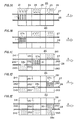
- FIG. 1A to Fig. 1F are block diagrams typically showing states of a crystal growth boat in liquid-phase epitaxial steps in an embodiment of a method of manufacturing a group III-V compound semiconductor solar battery according to the present invention.
- a crystal growth boat 20 has three storage regions 24, 25 and 26.
- the storage region 24 has first, second and third chambers 241, 242 and 243 which serve as receptacles for an n-type GaAs saturated solution 21 containing Sn or Te etc. as an n-type impurity.
- the storage region 25 has first, second and third chambers 251, 252 and 253 which serve as receptacles for an undoped GaAs supersaturated solution 22.
- the storage region 26 has first, second and third chambers 261, 262 and 263 which serve as receptacles for a p-type Al x Ga 1-x As saturated solution 23 containing Mg etc. as a p-type impurity.
- the first, second and third chambers in each of the storage regions 24, 25 and 26 are separated by sliders 27 and 28 having holes 27a and 28a respectively.
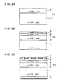
- Fig. 2A to Fig. 2C are sectional views showing a structure of a GaAs solar battery in respective steps in the embodiment of the inventive method of manufacturing a group III-V compound semiconductor solar battery.
- Fig. 1A to Fig. 1E and Fig. 2A to Fig. 2C description is now made on a method of manufacturing a GaAs solar battery according to the embodiment of the present invention.
- the crystal growth boat 20 has the n-type GaAs saturated solution 21, the undoped GaAs supersaturated solution 22 and the p-type Al x Ga 1-x As saturated solution 23 in the first chambers 241, 251 and 261 respectively, as shown in Fig. 1A.
- the sliders 27 and 28 are moved in a direction A, thereby to dip a n-type GaAs crystal substrate 1 doped with Si and having carrier density of 1 x 1017 cm ⁇ 3 to 2 x 1018cm ⁇ 3 in the n-type GaAs saturated solution 21 flowing into the sound chamber 242 through the hole 27a of the slider 27. Thereafter, the temperature of the n-type GaAs saturated solution 21 is lowered from a prescribed temperature level to another prescribed temperature level, thereby to crystallize n-type GaAs doped with Sn or Te on the n-type GaAs crystal substrate 1.
- an epitaxial substrate 10, shown in Fig. 2A having an n-type GaAs epitaxial layer 2 serving as a buffer layer on the n-type GaAs crystal substrate 1 is obtained.
- the slider 28 is moved in the direction A, thereby to transfer the n-type GaAs saturated solution 21 in the second chamber 242 of the storage region 24 into the third chamber 243 through the hole 28a of the slider 28.
- the n-type GaAs epitaxial substrate 10 having the n-type GaAs epitaxial layer 2 is still in the second chamber 242 of the storage region 24.
- the second chambers 242, 252 and 262 of the storage regions 24, 25 and 26 are slidingly moved in the direction A so that the second chamber 242 of the storage region 24, storing the n-type GaAs epitaxial substrate 10, becomes the second chamber 252 of the storage region 25 and the second chamber 252 of the storage region 25 becomes the second chamber 262 of the storage region 26.
- the slider 27 is moved in the direction A, thereby to dip the n-type GaAs epitaxial substrate 10 in the undoped GaAs supersaturated solution 22 flowing from the first chamber 251 of the storage region 25 into the second chamber 252 through the hole 27a of the slider 27. This state is maintained for a prescribed time at a prescribed temperature.
- the slider 28 is moved in the direction A thereby to transfer the undoped GaAs supersaturated solution 22 in the second chamber 252 of the storage region 25 to the third chamber 253 through the hole 28a of the slider 28, as shown in Fig. 1D.
- the n-type GaAs epitaxial substrate 10 is still in the second chamber 252 of the storage region 25.
- the second chambers 242, 252 and 262 of the storage regions 24, 25 and 26 are slidingly moved in the direction A, so that the second chamber 252 of the storage region 25, storing the n-type GaAs epitaxial substrate 10, becomes the second chamber 262 of the storage region 26.
- the slider 27 is moved in the direction A, thereby to dip the n- type GaAs epitaxial substrate 10 in the p-type Al x Ga 1-x As saturated solution 23 containing Mg as a p-type impurity, which has flown from the first chamber 261 of the storage region 26 into the second chamber 262 through the hole 27a of the slider 27.
- n-type GaAs epitaxial substrate 10 While the n-type GaAs epitaxial substrate 10 is dipped in the p-type Al x Ga 1-x As saturated solution 23 for a prescribed time in the second chamber 262 of the storage region 26, atoms of Mg, which are the p-type impurity contained in the p-type Al x Ga 1-x As saturated solution 23, are diffused in the n-type GaAs epitaxial layer 2 doped with Sn or Te on the n-type GaAs epitaxial substrate 10, whereby the surface portion of the layer 2 is inverted into a p-type.
- a p-type GaAs layer 4 shown in Fig. 2B is formed and a p-n junction region 3 is defined between the same and the n-type GaAs epitaxial layer 2.
- This p-n junction region 3 serves as a main photocell p-n junction region for the solar battery.
- the p-type Al x Ga 1-x As saturated solution 23 is transferred from the second chamber 262 of the storage region 26 to the third chamber 263 through the hole 28a of the slider 28, whereby the growth of the p-type Al x Ga 1-x As epitaxial layer 5 is terminated.
- a GaAs solar battery epitaxial substrate 30 which has the p-type GaAs layer 4 of high quality formed by diffusion of Mg atoms serving as the p-type impurity, and the p-type Al x Ga 1-x As layer 5.
- CVD chemical vapor deposition
- the n-type GaAs saturated solution 21 can be prevented from being mixed into the p-type Al x Ga 1-x As saturated solution 23 by the undoped GaAs supersaturated solution 22. Therefore, dispersion of the p-type Al x Ga 1-x As saturated solution 23 for each lot can be reduced when the epitaxial growth step is performed for each lot of the n-type GaAs crystal substrate 1. Thus, this method is excellent in control and stability of the p-n junction characteristic.
- Mg has low vapor pressure as compared with zinc (Zn)
- substantially no evaporation takes place during epitaxial growth and dispersion in thickness of the p-type GaAs layer 4 for each lot is small, whereby a GaAs solar battery having stable characteristics and excellent reliability can be obtained.
- the undoped GaAs supersaturated solution 22 is employed in the above embodiment to prevent mixing of the n-type GaAs saturated solution 21 into the p-type Al x Ga 1-x As saturated solution 23, an undoped GaAs saturated solution may be employed to attain a similar effect.
- a saturated solution such as an n-type GaAs saturated solution employed in a preceding liquid-phase epitaxial growth step is prevented from being mixed into a saturated solution such as a p-type Al x Ga 1-x As saturated solution employed in a later liquid-phase epitaxial growth step, so that contamination of the latter solution is prevented. Therefore, a group III-V compound semiconductor solar battery, such as a GaAs solar battery, of high conversion efficiency can be obtained, whose electric characteristic is not deteriorated even if the number of times of crystallization is increased.
Landscapes
- Photovoltaic Devices (AREA)
- Crystals, And After-Treatments Of Crystals (AREA)
Applications Claiming Priority (2)
| Application Number | Priority Date | Filing Date | Title |
|---|---|---|---|
| JP309797/86 | 1986-12-24 | ||
| JP61309797A JPS63160384A (ja) | 1986-12-24 | 1986-12-24 | GaAs太陽電池の製造方法 |
Publications (3)
| Publication Number | Publication Date |
|---|---|
| EP0272636A2 true EP0272636A2 (fr) | 1988-06-29 |
| EP0272636A3 EP0272636A3 (en) | 1988-10-26 |
| EP0272636B1 EP0272636B1 (fr) | 1991-04-24 |
Family
ID=17997356
Family Applications (1)
| Application Number | Title | Priority Date | Filing Date |
|---|---|---|---|
| EP87118767A Expired - Lifetime EP0272636B1 (fr) | 1986-12-24 | 1987-12-17 | Procédé de fabrication d'une cellule solaire avec composés semi-conducteurs III-V |
Country Status (4)
| Country | Link |
|---|---|
| US (1) | US4775639A (fr) |
| EP (1) | EP0272636B1 (fr) |
| JP (1) | JPS63160384A (fr) |
| DE (1) | DE3769616D1 (fr) |
Cited By (2)
| Publication number | Priority date | Publication date | Assignee | Title |
|---|---|---|---|---|
| EP0851513A3 (fr) * | 1996-12-27 | 1999-11-03 | Canon Kabushiki Kaisha | Méthode de fabrication d'un composant semiconducteur et méthode de fabrication d'une cellule solaire |
| US6756289B1 (en) | 1996-12-27 | 2004-06-29 | Canon Kabushiki Kaisha | Method of producing semiconductor member and method of producing solar cell |
Families Citing this family (12)
| Publication number | Priority date | Publication date | Assignee | Title |
|---|---|---|---|---|
| US5068695A (en) * | 1988-04-29 | 1991-11-26 | Sri International | Low dislocation density semiconductor device |
| US6613162B1 (en) * | 1999-10-25 | 2003-09-02 | Rensselaer Polytechnic Institute | Multicomponent homogeneous alloys and method for making same |
| US7641733B2 (en) * | 2004-09-01 | 2010-01-05 | Rensselaer Polytechnic Institute | Method and apparatus for growth of multi-component single crystals |
| EP2351097A2 (fr) | 2008-10-23 | 2011-08-03 | Alta Devices, Inc. | Dispositif photovoltaïque |
| US9691921B2 (en) * | 2009-10-14 | 2017-06-27 | Alta Devices, Inc. | Textured metallic back reflector |
| US9502594B2 (en) | 2012-01-19 | 2016-11-22 | Alta Devices, Inc. | Thin-film semiconductor optoelectronic device with textured front and/or back surface prepared from template layer and etching |
| US9768329B1 (en) | 2009-10-23 | 2017-09-19 | Alta Devices, Inc. | Multi-junction optoelectronic device |
| US20150380576A1 (en) * | 2010-10-13 | 2015-12-31 | Alta Devices, Inc. | Optoelectronic device with dielectric layer and method of manufacture |
| US9136422B1 (en) | 2012-01-19 | 2015-09-15 | Alta Devices, Inc. | Texturing a layer in an optoelectronic device for improved angle randomization of light |
| US20170141256A1 (en) | 2009-10-23 | 2017-05-18 | Alta Devices, Inc. | Multi-junction optoelectronic device with group iv semiconductor as a bottom junction |
| US11271128B2 (en) | 2009-10-23 | 2022-03-08 | Utica Leaseco, Llc | Multi-junction optoelectronic device |
| US11038080B2 (en) | 2012-01-19 | 2021-06-15 | Utica Leaseco, Llc | Thin-film semiconductor optoelectronic device with textured front and/or back surface prepared from etching |
Family Cites Families (4)
| Publication number | Priority date | Publication date | Assignee | Title |
|---|---|---|---|---|
| US4126930A (en) * | 1975-06-19 | 1978-11-28 | Varian Associates, Inc. | Magnesium doping of AlGaAs |
| US4178195A (en) * | 1976-11-22 | 1979-12-11 | International Business Machines Corporation | Semiconductor structure |
| US4235651A (en) * | 1979-03-19 | 1980-11-25 | Hughes Aircraft Company | Fabrication of GaAs-GaAlAs solar cells |
| JPS5683933A (en) * | 1979-12-13 | 1981-07-08 | Sharp Corp | Liquid phase epitaxial growth |
-
1986
- 1986-12-24 JP JP61309797A patent/JPS63160384A/ja active Pending
-
1987
- 1987-12-17 EP EP87118767A patent/EP0272636B1/fr not_active Expired - Lifetime
- 1987-12-17 DE DE8787118767T patent/DE3769616D1/de not_active Expired - Lifetime
- 1987-12-18 US US07/135,076 patent/US4775639A/en not_active Expired - Lifetime
Non-Patent Citations (4)
| Title |
|---|
| IEE JOURNAL ON SOLID-STATE AND ELECTRON DEVICES, vol. 1, no. 2, January 1977, pages 53-56, IEE, Stevenage, Herts, GB; P.W. ROSS et al.: "Heterojunction GaAs/GaAlAs transistors with enhanced gain from avalanche multiplication" * |
| KRISTALL UND TECHNIK, vol. 11, no. 10, October 1976, pages 1013-1020; Z.I. ALFEROV et al.: "Investigation of a new LPE method of obtaining Al-Ga-As heterostructures" * |
| SOVIET PHYSICS TECHNICAL PHYSICS, vol. 30, no. 6, June 1985, pages 645-643, American Institute of Physics, New York, US; V.M. ANDREEV et al.: "Influence of transition layers on the spectral sensitivity of AlGaAs heterophotocells * |
| THE CONFERENCE RECORD OF THE TWELFTH IEEE PHOTOVOLTAIC SPECIALISTS CONFERENCE-1976, Baton Rouge, Louisiana, 15th - 18th November 1976, pages 929-933; G.S. KAMATH et al.: "High efficiency and large area (GaA1)As-GaAs solar cells" * |
Cited By (3)
| Publication number | Priority date | Publication date | Assignee | Title |
|---|---|---|---|---|
| EP0851513A3 (fr) * | 1996-12-27 | 1999-11-03 | Canon Kabushiki Kaisha | Méthode de fabrication d'un composant semiconducteur et méthode de fabrication d'une cellule solaire |
| US6190937B1 (en) | 1996-12-27 | 2001-02-20 | Canon Kabushiki Kaisha | Method of producing semiconductor member and method of producing solar cell |
| US6756289B1 (en) | 1996-12-27 | 2004-06-29 | Canon Kabushiki Kaisha | Method of producing semiconductor member and method of producing solar cell |
Also Published As
| Publication number | Publication date |
|---|---|
| DE3769616D1 (de) | 1991-05-29 |
| EP0272636B1 (fr) | 1991-04-24 |
| EP0272636A3 (en) | 1988-10-26 |
| JPS63160384A (ja) | 1988-07-04 |
| US4775639A (en) | 1988-10-04 |
Similar Documents
| Publication | Publication Date | Title |
|---|---|---|
| US4159354A (en) | Method for making thin film III-V compound semiconductors for solar cells involving the use of a molten intermediate layer | |
| US5356509A (en) | Hetero-epitaxial growth of non-lattice matched semiconductors | |
| US4775639A (en) | Method of manufacturing Group III-V compound semiconductor solar battery | |
| US4876210A (en) | Solution growth of lattice mismatched and solubility mismatched heterostructures | |
| US4451691A (en) | Three-terminal ternary III-V multicolor solar cells and process of fabrication | |
| US4156310A (en) | High bandgap window layer for gaas solar cells and fabrication process therefor | |
| US4575577A (en) | Ternary III-V multicolor solar cells containing a quaternary window layer and a quaternary transition layer | |
| JPS63169717A (ja) | 半導体素子 | |
| US4039357A (en) | Etching of III-V semiconductor materials with H2 S in the preparation of heterodiodes to facilitate the deposition of cadmium sulfide | |
| US4479222A (en) | Diffusion barrier for long wavelength laser diodes | |
| US3960618A (en) | Epitaxial growth process for compound semiconductor crystals in liquid phase | |
| US4504329A (en) | Process for the epitaxial deposition of III-V compounds utilizing a binary alloy as the metallic source | |
| US20110048537A1 (en) | Method of fabricating a semiconductor junction | |
| US4216484A (en) | Method of manufacturing electroluminescent compound semiconductor wafer | |
| US4235651A (en) | Fabrication of GaAs-GaAlAs solar cells | |
| US3676228A (en) | Method of making a p-n junction device | |
| US4163987A (en) | GaAs-GaAlAs solar cells | |
| JPH08335715A (ja) | エピタキシャルウエハおよびその製造方法 | |
| US4087293A (en) | Silicon as donor dopant in Hg1-x Cdx Te | |
| US3619304A (en) | Method of manufacturing gallium phosphide electro luminescent diodes | |
| US3959036A (en) | Method for the production of a germanium doped gas contact layer | |
| CA1333248C (fr) | Methode de formation de cristaux | |
| JPS6350851B2 (fr) | ||
| US5254211A (en) | Method for forming crystals | |
| Corkish | Some candidate materials for lattice-matched liquid-phase epitaxial growth on silicon |
Legal Events
| Date | Code | Title | Description |
|---|---|---|---|
| PUAI | Public reference made under article 153(3) epc to a published international application that has entered the european phase |
Free format text: ORIGINAL CODE: 0009012 |
|
| AK | Designated contracting states |
Kind code of ref document: A2 Designated state(s): DE FR IT |
|
| PUAL | Search report despatched |
Free format text: ORIGINAL CODE: 0009013 |
|
| AK | Designated contracting states |
Kind code of ref document: A3 Designated state(s): DE FR IT |
|
| 17P | Request for examination filed |
Effective date: 19881230 |
|
| 17Q | First examination report despatched |
Effective date: 19900808 |
|
| GRAA | (expected) grant |
Free format text: ORIGINAL CODE: 0009210 |
|
| AK | Designated contracting states |
Kind code of ref document: B1 Designated state(s): DE FR IT |
|
| ITF | It: translation for a ep patent filed | ||
| REF | Corresponds to: |
Ref document number: 3769616 Country of ref document: DE Date of ref document: 19910529 |
|
| ET | Fr: translation filed | ||
| PLBE | No opposition filed within time limit |
Free format text: ORIGINAL CODE: 0009261 |
|
| STAA | Information on the status of an ep patent application or granted ep patent |
Free format text: STATUS: NO OPPOSITION FILED WITHIN TIME LIMIT |
|
| 26N | No opposition filed | ||
| REG | Reference to a national code |
Ref country code: FR Ref legal event code: D6 |
|
| ITPR | It: changes in ownership of a european patent |
Owner name: OFFERTA DI LICENZA AL PUBBLICO |
|
| PGFP | Annual fee paid to national office [announced via postgrant information from national office to epo] |
Ref country code: FR Payment date: 20041208 Year of fee payment: 18 |
|
| PGFP | Annual fee paid to national office [announced via postgrant information from national office to epo] |
Ref country code: DE Payment date: 20041209 Year of fee payment: 18 |
|
| PG25 | Lapsed in a contracting state [announced via postgrant information from national office to epo] |
Ref country code: IT Free format text: LAPSE BECAUSE OF NON-PAYMENT OF DUE FEES;WARNING: LAPSES OF ITALIAN PATENTS WITH EFFECTIVE DATE BEFORE 2007 MAY HAVE OCCURRED AT ANY TIME BEFORE 2007. THE CORRECT EFFECTIVE DATE MAY BE DIFFERENT FROM THE ONE RECORDED. Effective date: 20051217 |
|
| PG25 | Lapsed in a contracting state [announced via postgrant information from national office to epo] |
Ref country code: DE Free format text: LAPSE BECAUSE OF NON-PAYMENT OF DUE FEES Effective date: 20060701 |
|
| PG25 | Lapsed in a contracting state [announced via postgrant information from national office to epo] |
Ref country code: FR Free format text: LAPSE BECAUSE OF NON-PAYMENT OF DUE FEES Effective date: 20060831 |
|
| REG | Reference to a national code |
Ref country code: FR Ref legal event code: ST Effective date: 20060831 |