EP0272678A2 - Methode zur Herstellung leitfähiger Muster und ihre Anwendungen - Google Patents
Methode zur Herstellung leitfähiger Muster und ihre Anwendungen Download PDFInfo
- Publication number
- EP0272678A2 EP0272678A2 EP87118977A EP87118977A EP0272678A2 EP 0272678 A2 EP0272678 A2 EP 0272678A2 EP 87118977 A EP87118977 A EP 87118977A EP 87118977 A EP87118977 A EP 87118977A EP 0272678 A2 EP0272678 A2 EP 0272678A2
- Authority
- EP
- European Patent Office
- Prior art keywords
- pattern
- conductive film
- substrate
- chip
- pads
- Prior art date
- Legal status (The legal status is an assumption and is not a legal conclusion. Google has not performed a legal analysis and makes no representation as to the accuracy of the status listed.)
- Withdrawn
Links
Images


Classifications
-
- G—PHYSICS
- G02—OPTICS
- G02F—OPTICAL DEVICES OR ARRANGEMENTS FOR THE CONTROL OF LIGHT BY MODIFICATION OF THE OPTICAL PROPERTIES OF THE MEDIA OF THE ELEMENTS INVOLVED THEREIN; NON-LINEAR OPTICS; FREQUENCY-CHANGING OF LIGHT; OPTICAL LOGIC ELEMENTS; OPTICAL ANALOGUE/DIGITAL CONVERTERS
- G02F1/00—Devices or arrangements for the control of the intensity, colour, phase, polarisation or direction of light arriving from an independent light source, e.g. switching, gating or modulating; Non-linear optics
- G02F1/01—Devices or arrangements for the control of the intensity, colour, phase, polarisation or direction of light arriving from an independent light source, e.g. switching, gating or modulating; Non-linear optics for the control of the intensity, phase, polarisation or colour
- G02F1/13—Devices or arrangements for the control of the intensity, colour, phase, polarisation or direction of light arriving from an independent light source, e.g. switching, gating or modulating; Non-linear optics for the control of the intensity, phase, polarisation or colour based on liquid crystals, e.g. single liquid crystal display cells
- G02F1/133—Constructional arrangements; Operation of liquid crystal cells; Circuit arrangements
- G02F1/1333—Constructional arrangements; Manufacturing methods
- G02F1/1345—Conductors connecting electrodes to cell terminals
- G02F1/13452—Conductors connecting driver circuitry and terminals of panels
-
- G—PHYSICS
- G02—OPTICS
- G02F—OPTICAL DEVICES OR ARRANGEMENTS FOR THE CONTROL OF LIGHT BY MODIFICATION OF THE OPTICAL PROPERTIES OF THE MEDIA OF THE ELEMENTS INVOLVED THEREIN; NON-LINEAR OPTICS; FREQUENCY-CHANGING OF LIGHT; OPTICAL LOGIC ELEMENTS; OPTICAL ANALOGUE/DIGITAL CONVERTERS
- G02F1/00—Devices or arrangements for the control of the intensity, colour, phase, polarisation or direction of light arriving from an independent light source, e.g. switching, gating or modulating; Non-linear optics
- G02F1/01—Devices or arrangements for the control of the intensity, colour, phase, polarisation or direction of light arriving from an independent light source, e.g. switching, gating or modulating; Non-linear optics for the control of the intensity, phase, polarisation or colour
- G02F1/13—Devices or arrangements for the control of the intensity, colour, phase, polarisation or direction of light arriving from an independent light source, e.g. switching, gating or modulating; Non-linear optics for the control of the intensity, phase, polarisation or colour based on liquid crystals, e.g. single liquid crystal display cells
- G02F1/133—Constructional arrangements; Operation of liquid crystal cells; Circuit arrangements
- G02F1/1333—Constructional arrangements; Manufacturing methods
- G02F1/1343—Electrodes
- G02F1/13439—Electrodes characterised by their electrical, optical, physical properties; materials therefor; method of making
-
- G—PHYSICS
- G02—OPTICS
- G02F—OPTICAL DEVICES OR ARRANGEMENTS FOR THE CONTROL OF LIGHT BY MODIFICATION OF THE OPTICAL PROPERTIES OF THE MEDIA OF THE ELEMENTS INVOLVED THEREIN; NON-LINEAR OPTICS; FREQUENCY-CHANGING OF LIGHT; OPTICAL LOGIC ELEMENTS; OPTICAL ANALOGUE/DIGITAL CONVERTERS
- G02F1/00—Devices or arrangements for the control of the intensity, colour, phase, polarisation or direction of light arriving from an independent light source, e.g. switching, gating or modulating; Non-linear optics
- G02F1/01—Devices or arrangements for the control of the intensity, colour, phase, polarisation or direction of light arriving from an independent light source, e.g. switching, gating or modulating; Non-linear optics for the control of the intensity, phase, polarisation or colour
- G02F1/13—Devices or arrangements for the control of the intensity, colour, phase, polarisation or direction of light arriving from an independent light source, e.g. switching, gating or modulating; Non-linear optics for the control of the intensity, phase, polarisation or colour based on liquid crystals, e.g. single liquid crystal display cells
- G02F1/133—Constructional arrangements; Operation of liquid crystal cells; Circuit arrangements
- G02F1/1333—Constructional arrangements; Manufacturing methods
- G02F1/1345—Conductors connecting electrodes to cell terminals
-
- H—ELECTRICITY
- H05—ELECTRIC TECHNIQUES NOT OTHERWISE PROVIDED FOR
- H05K—PRINTED CIRCUITS; CASINGS OR CONSTRUCTIONAL DETAILS OF ELECTRIC APPARATUS; MANUFACTURE OF ASSEMBLAGES OF ELECTRICAL COMPONENTS
- H05K3/00—Apparatus or processes for manufacturing printed circuits
- H05K3/22—Secondary treatment of printed circuits
- H05K3/24—Reinforcing of the conductive pattern
- H05K3/245—Reinforcing conductive patterns made by printing techniques or by other techniques for applying conductive pastes, inks or powders; Reinforcing other conductive patterns by such techniques
-
- H—ELECTRICITY
- H10—SEMICONDUCTOR DEVICES; ELECTRIC SOLID-STATE DEVICES NOT OTHERWISE PROVIDED FOR
- H10W—GENERIC PACKAGES, INTERCONNECTIONS, CONNECTORS OR OTHER CONSTRUCTIONAL DETAILS OF DEVICES COVERED BY CLASS H10
- H10W70/00—Package substrates; Interposers; Redistribution layers [RDL]
- H10W70/01—Manufacture or treatment
- H10W70/05—Manufacture or treatment of insulating or insulated package substrates, or of interposers, or of redistribution layers
- H10W70/098—Applying pastes or inks, e.g. screen printing
-
- H—ELECTRICITY
- H05—ELECTRIC TECHNIQUES NOT OTHERWISE PROVIDED FOR
- H05K—PRINTED CIRCUITS; CASINGS OR CONSTRUCTIONAL DETAILS OF ELECTRIC APPARATUS; MANUFACTURE OF ASSEMBLAGES OF ELECTRICAL COMPONENTS
- H05K1/00—Printed circuits
- H05K1/02—Details
- H05K1/09—Use of materials for the conductive, e.g. metallic pattern
- H05K1/092—Dispersed materials, e.g. conductive pastes or inks
- H05K1/095—Dispersed materials, e.g. conductive pastes or inks for polymer thick films, i.e. having a permanent organic polymeric binder
-
- H—ELECTRICITY
- H05—ELECTRIC TECHNIQUES NOT OTHERWISE PROVIDED FOR
- H05K—PRINTED CIRCUITS; CASINGS OR CONSTRUCTIONAL DETAILS OF ELECTRIC APPARATUS; MANUFACTURE OF ASSEMBLAGES OF ELECTRICAL COMPONENTS
- H05K2201/00—Indexing scheme relating to printed circuits covered by H05K1/00
- H05K2201/03—Conductive materials
- H05K2201/032—Materials
- H05K2201/0326—Inorganic, non-metallic conductor, e.g. indium-tin oxide [ITO]
-
- H—ELECTRICITY
- H05—ELECTRIC TECHNIQUES NOT OTHERWISE PROVIDED FOR
- H05K—PRINTED CIRCUITS; CASINGS OR CONSTRUCTIONAL DETAILS OF ELECTRIC APPARATUS; MANUFACTURE OF ASSEMBLAGES OF ELECTRICAL COMPONENTS
- H05K2201/00—Indexing scheme relating to printed circuits covered by H05K1/00
- H05K2201/03—Conductive materials
- H05K2201/0332—Structure of the conductor
- H05K2201/0335—Layered conductors or foils
- H05K2201/035—Paste overlayer, i.e. conductive paste or solder paste over conductive layer
-
- H—ELECTRICITY
- H10—SEMICONDUCTOR DEVICES; ELECTRIC SOLID-STATE DEVICES NOT OTHERWISE PROVIDED FOR
- H10W—GENERIC PACKAGES, INTERCONNECTIONS, CONNECTORS OR OTHER CONSTRUCTIONAL DETAILS OF DEVICES COVERED BY CLASS H10
- H10W72/00—Interconnections or connectors in packages
- H10W72/071—Connecting or disconnecting
- H10W72/072—Connecting or disconnecting of bump connectors
-
- H—ELECTRICITY
- H10—SEMICONDUCTOR DEVICES; ELECTRIC SOLID-STATE DEVICES NOT OTHERWISE PROVIDED FOR
- H10W—GENERIC PACKAGES, INTERCONNECTIONS, CONNECTORS OR OTHER CONSTRUCTIONAL DETAILS OF DEVICES COVERED BY CLASS H10
- H10W72/00—Interconnections or connectors in packages
- H10W72/071—Connecting or disconnecting
- H10W72/074—Connecting or disconnecting of anisotropic conductive adhesives
-
- H—ELECTRICITY
- H10—SEMICONDUCTOR DEVICES; ELECTRIC SOLID-STATE DEVICES NOT OTHERWISE PROVIDED FOR
- H10W—GENERIC PACKAGES, INTERCONNECTIONS, CONNECTORS OR OTHER CONSTRUCTIONAL DETAILS OF DEVICES COVERED BY CLASS H10
- H10W72/00—Interconnections or connectors in packages
- H10W72/20—Bump connectors, e.g. solder bumps or copper pillars; Dummy bumps; Thermal bumps
- H10W72/241—Dispositions, e.g. layouts
-
- H—ELECTRICITY
- H10—SEMICONDUCTOR DEVICES; ELECTRIC SOLID-STATE DEVICES NOT OTHERWISE PROVIDED FOR
- H10W—GENERIC PACKAGES, INTERCONNECTIONS, CONNECTORS OR OTHER CONSTRUCTIONAL DETAILS OF DEVICES COVERED BY CLASS H10
- H10W72/00—Interconnections or connectors in packages
- H10W72/30—Die-attach connectors
- H10W72/321—Structures or relative sizes of die-attach connectors
- H10W72/325—Die-attach connectors having a filler embedded in a matrix
-
- H—ELECTRICITY
- H10—SEMICONDUCTOR DEVICES; ELECTRIC SOLID-STATE DEVICES NOT OTHERWISE PROVIDED FOR
- H10W—GENERIC PACKAGES, INTERCONNECTIONS, CONNECTORS OR OTHER CONSTRUCTIONAL DETAILS OF DEVICES COVERED BY CLASS H10
- H10W72/00—Interconnections or connectors in packages
- H10W72/30—Die-attach connectors
- H10W72/351—Materials of die-attach connectors
- H10W72/352—Materials of die-attach connectors comprising metals or metalloids, e.g. solders
-
- H—ELECTRICITY
- H10—SEMICONDUCTOR DEVICES; ELECTRIC SOLID-STATE DEVICES NOT OTHERWISE PROVIDED FOR
- H10W—GENERIC PACKAGES, INTERCONNECTIONS, CONNECTORS OR OTHER CONSTRUCTIONAL DETAILS OF DEVICES COVERED BY CLASS H10
- H10W72/00—Interconnections or connectors in packages
- H10W72/30—Die-attach connectors
- H10W72/351—Materials of die-attach connectors
- H10W72/353—Materials of die-attach connectors not comprising solid metals or solid metalloids, e.g. ceramics
- H10W72/354—Materials of die-attach connectors not comprising solid metals or solid metalloids, e.g. ceramics comprising polymers
-
- Y—GENERAL TAGGING OF NEW TECHNOLOGICAL DEVELOPMENTS; GENERAL TAGGING OF CROSS-SECTIONAL TECHNOLOGIES SPANNING OVER SEVERAL SECTIONS OF THE IPC; TECHNICAL SUBJECTS COVERED BY FORMER USPC CROSS-REFERENCE ART COLLECTIONS [XRACs] AND DIGESTS
- Y10—TECHNICAL SUBJECTS COVERED BY FORMER USPC
- Y10T—TECHNICAL SUBJECTS COVERED BY FORMER US CLASSIFICATION
- Y10T29/00—Metal working
- Y10T29/49—Method of mechanical manufacture
- Y10T29/49002—Electrical device making
- Y10T29/49117—Conductor or circuit manufacturing
- Y10T29/49124—On flat or curved insulated base, e.g., printed circuit, etc.
- Y10T29/4913—Assembling to base an electrical component, e.g., capacitor, etc.
-
- Y—GENERAL TAGGING OF NEW TECHNOLOGICAL DEVELOPMENTS; GENERAL TAGGING OF CROSS-SECTIONAL TECHNOLOGIES SPANNING OVER SEVERAL SECTIONS OF THE IPC; TECHNICAL SUBJECTS COVERED BY FORMER USPC CROSS-REFERENCE ART COLLECTIONS [XRACs] AND DIGESTS
- Y10—TECHNICAL SUBJECTS COVERED BY FORMER USPC
- Y10T—TECHNICAL SUBJECTS COVERED BY FORMER US CLASSIFICATION
- Y10T29/00—Metal working
- Y10T29/49—Method of mechanical manufacture
- Y10T29/49002—Electrical device making
- Y10T29/49117—Conductor or circuit manufacturing
- Y10T29/49124—On flat or curved insulated base, e.g., printed circuit, etc.
- Y10T29/4913—Assembling to base an electrical component, e.g., capacitor, etc.
- Y10T29/49133—Assembling to base an electrical component, e.g., capacitor, etc. with component orienting
- Y10T29/49137—Different components
-
- Y—GENERAL TAGGING OF NEW TECHNOLOGICAL DEVELOPMENTS; GENERAL TAGGING OF CROSS-SECTIONAL TECHNOLOGIES SPANNING OVER SEVERAL SECTIONS OF THE IPC; TECHNICAL SUBJECTS COVERED BY FORMER USPC CROSS-REFERENCE ART COLLECTIONS [XRACs] AND DIGESTS
- Y10—TECHNICAL SUBJECTS COVERED BY FORMER USPC
- Y10T—TECHNICAL SUBJECTS COVERED BY FORMER US CLASSIFICATION
- Y10T29/00—Metal working
- Y10T29/49—Method of mechanical manufacture
- Y10T29/49002—Electrical device making
- Y10T29/49117—Conductor or circuit manufacturing
- Y10T29/49124—On flat or curved insulated base, e.g., printed circuit, etc.
- Y10T29/49155—Manufacturing circuit on or in base
Definitions
- This invention relates to a conductive pattern producing method, and more particularly, relates to an improvement for conductive pattern producing method which makes the pattern thus produced by the method more credible.
- the interest of operators to manufacture liquid crystal devices which comprises a pair of glass substrates and electrode pattern including addressing lines and signal lines for producing a matrix arragement, is directed to how to form a pattern on the substrates without deffect and with a high reliability of the pattern.
- the device generally includes an IC chip for driving the liquid crystal device.
- the facilitataion and credibility of the connection between the IC chip and the pattern is alway in question. Particularly, in the case that a pattern is formed on a glass substrate, there likely occur fissures in the pattern which cause disconnection of circuitry.
- patterns are manufactured with double-layered film.
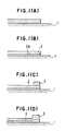
- a method of forming a conductive pattern on a substrate for mounting thereon an IC chip in accordance with the present invention On a glass substrate for liquid crystal device, only a portion of which is illustrated in the figures, a conductive pattern is formed by offset screen printing with a conductive paste (Fig.1(A)).
- the conductive paste for the pattern is prepared by mixing, with an oil emulsion, "cover silver paste” (Prod No. 61900234) distributed by Detmeron, a manufacture of FRG.
- the thickness of the pattern is 10 microns.
- the substrate is baked in a nitrogen atmosphere in accordance with a temperature curve shown in Fig.4(A), so that formed are a contact region 2a and a sintered region largely consisting of silver (Fig.1(B)).
- another pattern to make a thick portion is formed in the same manner by printing and baking (Figs.1(C) and 1(D)).
- the thickness of the thick portion is 30 microns after baking.
- the pattern can be formed of ITO by sputtering with a good contact and a good conductivity.
- Figs.2(A) and 2(B) are plan view and a cross sectional view showing the whole pattern on the substrate formed as explaned above.
- a transparent adhesive of epoxy resin mixed with Ni particles having 15 microns in average diameter is applied to the surface of the substrate which is to face the bottom surface and the electrode pads of an IC.
- the Ni particles are added into at 50 mg per each 5g of the adhesive.
- the IC chip is mounted on the substrate with its aluminium pads contacting corresponding pads of the thick portion of the pattern, and the epoxy resin is hardened at 180 °C while pressing the IC against the substrate for 20 munities with a force of 3 Kg using a jig.
- the alignment of the pads of the IC chip with the pattern on the substrate is checked by viewing the both from the bottom of the substrate through the transparent resin.
- a resin which can be cured by a UV light may be also used as the adhesive.
- the resin is irradiated with a UV light through the transparent substrate.
- Fig.3(A) is a partial cross section view showing the contact of the IC chip 5 with the substrate 1 after the hardening of the epoxy adhesive.
- the distance between the A1 pad 8 and the top of the thick portion 3 is designed 3 microns in which the Ni particles are caught and make the resistance of the contact low.
- Other particles contained in the epoxy resin are situated between the IC chip and the substrate with 30 microns in distance, and do not damage the IC chip and the pattern 2 on the substrate 1.
- the area of the thick portion is preferably smaller than that of the corresponding pad of the pattern.
- a thick portion 3 is formed by coating the prescribed portion with DAP1 (No.61901143), a conductive adhesive distributed by Detmeron. Then, the IC chip is mounted on the substrate with its aluminium pads contacting corresponding lands of the thick portion of the pattern and pressed against the substrate with a jig, and the substrate is baked in accordance with the temperature curve shown in Fig.4(B).
- Fig.3(B) is a cross sectional view showing the electrical connection between the IC chip and the pattern in accordance with this embodiment.
- a glass substrate 1 is coated by printing with a conductive paste consisting of Cu particles dispersed in a phenol resin, in order to form a prescribed pattern 11 comprising electrode lines for making contact with counterpart pads of the IC chip.
- the average diameter of the Cu particle is 5-10 microns.
- This conductive paste coating is then baked at 60 °C for 10 munites and becomes thin by shrinking. The baked layer 11 might have a fissure 12.
- Another layer 13 of the Cu conductive paste is superimposed over the layer 11 by printing on the baked Cu layer as shown in Fig.5(B).
- the overlying Cu layer is also baked at 60°C for 10 munites.
- the fissure 12 has to be mended by this overlying pattern.
- the dispersion of the double-layered pattern in thickness is about 30 microns.
- the double-layered pattern is then pressed to produce an even top surface 14.
- the thickness of the double-layered pattern becomes about 20 microns after pressing.
- On the pattern is mounted an IC chip whose electrode pads to be made contact with the patterns are given Au bumps by plating and the IC chip is pressed against the substrate with an adhesive resin securing the IC chip in place.
Landscapes
- Physics & Mathematics (AREA)
- Nonlinear Science (AREA)
- Crystallography & Structural Chemistry (AREA)
- Mathematical Physics (AREA)
- Chemical & Material Sciences (AREA)
- General Physics & Mathematics (AREA)
- Optics & Photonics (AREA)
- Engineering & Computer Science (AREA)
- Microelectronics & Electronic Packaging (AREA)
- Manufacturing & Machinery (AREA)
- Wire Bonding (AREA)
- Manufacturing Of Printed Wiring (AREA)
- Liquid Crystal (AREA)
Applications Claiming Priority (2)
| Application Number | Priority Date | Filing Date | Title |
|---|---|---|---|
| JP310493/86 | 1986-12-24 | ||
| JP61310493A JPS63160352A (ja) | 1986-12-24 | 1986-12-24 | 半導体装置の実装方法 |
Publications (2)
| Publication Number | Publication Date |
|---|---|
| EP0272678A2 true EP0272678A2 (de) | 1988-06-29 |
| EP0272678A3 EP0272678A3 (de) | 1990-04-25 |
Family
ID=18005889
Family Applications (1)
| Application Number | Title | Priority Date | Filing Date |
|---|---|---|---|
| EP87118977A Withdrawn EP0272678A3 (de) | 1986-12-24 | 1987-12-21 | Methode zur Herstellung leitfähiger Muster und ihre Anwendungen |
Country Status (4)
| Country | Link |
|---|---|
| US (3) | US6383327B1 (de) |
| EP (1) | EP0272678A3 (de) |
| JP (1) | JPS63160352A (de) |
| CN (1) | CN1021875C (de) |
Cited By (2)
| Publication number | Priority date | Publication date | Assignee | Title |
|---|---|---|---|---|
| US7916263B2 (en) | 2004-12-02 | 2011-03-29 | Semiconductor Energy Laboratory Co., Ltd. | Display device |
| EP2924695A4 (de) * | 2012-11-21 | 2016-01-27 | Sumitomo Riko Co Ltd | Flexibles leitendes element und wandler damit |
Families Citing this family (12)
| Publication number | Priority date | Publication date | Assignee | Title |
|---|---|---|---|---|
| US7411211B1 (en) * | 1999-07-22 | 2008-08-12 | Semiconductor Energy Laboratory Co., Ltd. | Contact structure and semiconductor device |
| JP2001053283A (ja) | 1999-08-12 | 2001-02-23 | Semiconductor Energy Lab Co Ltd | 半導体装置及びその作製方法 |
| US7361027B2 (en) * | 2002-12-25 | 2008-04-22 | Semiconductor Energy Laboratory Co., Ltd. | Contact structure, display device and electronic device |
| TWI265762B (en) * | 2003-01-14 | 2006-11-01 | Sharp Kk | Wiring material, wiring substrate and manufacturing method thereof, display panel, fine particle thin film material, substrate including thin film layer and manufacturing method thereof |
| DE102004019412A1 (de) * | 2004-04-19 | 2005-11-03 | Man Roland Druckmaschinen Ag | Verfahren zum Drucken elektrischer und/oder elektronischer Strukturen und Folie zur Verwendung in einem solchen Verfahren |
| US7276453B2 (en) * | 2004-08-10 | 2007-10-02 | E.I. Du Pont De Nemours And Company | Methods for forming an undercut region and electronic devices incorporating the same |
| US7166860B2 (en) * | 2004-12-30 | 2007-01-23 | E. I. Du Pont De Nemours And Company | Electronic device and process for forming same |
| KR101003585B1 (ko) * | 2008-06-25 | 2010-12-22 | 삼성전기주식회사 | 전자부품 내장형 인쇄회로기판 및 그 제조방법 |
| CN102332406B (zh) * | 2011-08-30 | 2015-12-09 | 华东光电集成器件研究所 | 集成电路导电胶图形制作方法 |
| KR101513642B1 (ko) * | 2013-08-21 | 2015-04-20 | 엘지전자 주식회사 | 반도체 디바이스 |
| KR101509425B1 (ko) | 2013-08-29 | 2015-04-08 | (주)에프씨아이 | 컨덕티브 필름을 포함하는 반도체 구조 |
| JP6434029B2 (ja) | 2013-09-06 | 2018-12-05 | ソルベイ スペシャルティ ポリマーズ イタリー エス.ピー.エー. | 導電性アセンブリ |
Family Cites Families (39)
| Publication number | Priority date | Publication date | Assignee | Title |
|---|---|---|---|---|
| US3079282A (en) * | 1960-05-24 | 1963-02-26 | Martin N Halier | Printed circuit on a ceramic base and method of making same |
| JPS557022B1 (de) * | 1968-05-10 | 1980-02-21 | ||
| US3892635A (en) * | 1971-10-28 | 1975-07-01 | Enthone | Pre-conditioner and process |
| NL163370C (nl) * | 1972-04-28 | 1980-08-15 | Philips Nv | Werkwijze voor het vervaardigen van een halfgeleider- inrichting met een geleiderpatroon. |
| US3983284A (en) * | 1972-06-02 | 1976-09-28 | Thomson-Csf | Flat connection for a semiconductor multilayer structure |
| US4113578A (en) * | 1973-05-31 | 1978-09-12 | Honeywell Inc. | Microcircuit device metallization |
| US4113981A (en) * | 1974-08-14 | 1978-09-12 | Kabushiki Kaisha Seikosha | Electrically conductive adhesive connecting arrays of conductors |
| JPS5182329A (en) * | 1975-01-17 | 1976-07-19 | Nippon Paint Co Ltd | Ototsumoyono totsuchobuno osaenarashihoho |
| JPS51102466A (en) * | 1975-03-06 | 1976-09-09 | Suwa Seikosha Kk | Handotaisoshinojitsusohoho |
| JPS5237744A (en) * | 1975-09-19 | 1977-03-23 | Seiko Epson Corp | Electronic desk computer with liquid crystal display |
| US4201801A (en) * | 1976-05-12 | 1980-05-06 | Nippon Paint Co., Ltd. | Method of forming a decorative relief pattern |
| JPS5392465A (en) * | 1977-01-24 | 1978-08-14 | Nippon Electric Co | Electronic circuit element board |
| US4427715A (en) * | 1978-07-03 | 1984-01-24 | National Semiconductor Corporation | Method of forming expanded pad structure |
| US4327124A (en) * | 1978-07-28 | 1982-04-27 | Desmarais Jr Raymond C | Method for manufacturing printed circuits comprising printing conductive ink on dielectric surface |
| US4297004A (en) * | 1978-09-20 | 1981-10-27 | Technical Research of Citizen Watch Co., Ltd. | Liquid crystal display cell |
| JPS5670529A (en) * | 1979-11-14 | 1981-06-12 | Hitachi Ltd | Liquid crystal display unit |
| ATE15734T1 (de) * | 1980-12-12 | 1985-10-15 | Prutec Ltd | Verfahren zum herstellen lichtelektrischer einrichtungen. |
| JPS589124A (ja) | 1981-07-09 | 1983-01-19 | Seiko Epson Corp | 液晶パネルの電極構造 |
| US4510179A (en) * | 1981-08-18 | 1985-04-09 | Matsushita Electric Industrial Co., Ltd. | Electrode on heat-resisting and isolating substrate and the manufacturing process for it |
| DE3136794C2 (de) * | 1981-09-16 | 1983-07-28 | Siemens AG, 1000 Berlin und 8000 München | Lötfähiges Schichtensystem, seine Verwendung und Verfahren zu seiner Herstellung |
| FR2516739A1 (fr) * | 1981-11-17 | 1983-05-20 | Rhone Poulenc Spec Chim | Procede de fabrication de circuits electroniques de type hybride a couches epaisses, des moyens destines a la mise en oeuvre de ce procede et les circuits obtenus selon ce procede |
| JPS58148434A (ja) | 1982-02-26 | 1983-09-03 | Mitsubishi Electric Corp | 電気部品実装基板の製造方法 |
| JPS58148934A (ja) * | 1982-03-02 | 1983-09-05 | Kokusai Denshin Denwa Co Ltd <Kdd> | 光伝送路の伝送特性測定方式 |
| JPS58148923A (ja) * | 1982-03-02 | 1983-09-05 | Seiko Instr & Electronics Ltd | 電子調律器 |
| FR2525209B1 (fr) * | 1982-04-16 | 1986-08-22 | Thomson Csf | Procede de realisation d'une couche composite metallique sur un substrat ceramique, et couche metallique obtenue par ce procede |
| NO157212C (no) * | 1982-09-21 | 1988-02-10 | Pilkington Brothers Plc | Fremgangsmaate for fremstilling av belegg med lav emisjonsevne. |
| JPS6092648A (ja) * | 1983-10-26 | 1985-05-24 | Matsushita Electric Ind Co Ltd | バンプ形成用基板およびこれを用いたバンプ形成方法 |
| JPS60107845A (ja) | 1983-11-17 | 1985-06-13 | Toshiba Corp | 半導体用回路基板 |
| JPS60108822A (ja) | 1983-11-18 | 1985-06-14 | Alps Electric Co Ltd | 液晶表示素子の端子接続方法 |
| JPS60179703A (ja) * | 1984-02-28 | 1985-09-13 | Seiko Instr & Electronics Ltd | 多色表示装置の製造方法 |
| JPS60180151A (ja) * | 1984-02-28 | 1985-09-13 | Narumi China Corp | バンプ付基板及びその製作法 |
| JPS60238817A (ja) * | 1984-05-12 | 1985-11-27 | Citizen Watch Co Ltd | 液晶表示装置 |
| JPS6149432A (ja) * | 1984-08-18 | 1986-03-11 | Matsushita Electric Ind Co Ltd | 半導体装置の製造方法 |
| JPS61173471A (ja) * | 1985-01-28 | 1986-08-05 | シャープ株式会社 | 熱圧着コネクタ− |
| JPS61256657A (ja) * | 1985-05-08 | 1986-11-14 | Mitsubishi Electric Corp | 厚膜形成方法 |
| JPS629642A (ja) * | 1985-07-05 | 1987-01-17 | Matsushita Electric Ind Co Ltd | 半導体装置の製造方法 |
| US4667401A (en) * | 1985-11-26 | 1987-05-26 | Clements James R | Method of making an electronic device using an uniaxial conductive adhesive |
| WO1990004263A1 (en) * | 1988-10-14 | 1990-04-19 | Matsushita Electric Industrial Co., Ltd. | Image sensor and method of producing the same |
| JPH10100303A (ja) * | 1996-06-07 | 1998-04-21 | Nippon Sheet Glass Co Ltd | 透明導電膜付き基板およびそれを用いた表示素子 |
-
1986
- 1986-12-24 JP JP61310493A patent/JPS63160352A/ja active Granted
-
1987
- 1987-12-21 EP EP87118977A patent/EP0272678A3/de not_active Withdrawn
- 1987-12-23 CN CN87105952.5A patent/CN1021875C/zh not_active Expired - Lifetime
-
1994
- 1994-03-30 US US08/219,853 patent/US6383327B1/en not_active Expired - Lifetime
-
2001
- 2001-11-26 US US09/995,866 patent/US20020110637A1/en not_active Abandoned
-
2005
- 2005-02-03 US US11/048,767 patent/US7288437B2/en not_active Expired - Fee Related
Cited By (4)
| Publication number | Priority date | Publication date | Assignee | Title |
|---|---|---|---|---|
| US7916263B2 (en) | 2004-12-02 | 2011-03-29 | Semiconductor Energy Laboratory Co., Ltd. | Display device |
| US8243220B2 (en) | 2004-12-02 | 2012-08-14 | Semiconductor Energy Laboratory Co., Ltd. | Display device |
| US9166190B2 (en) | 2004-12-02 | 2015-10-20 | Semiconductor Energy Laboratory Co., Ltd. | Display device |
| EP2924695A4 (de) * | 2012-11-21 | 2016-01-27 | Sumitomo Riko Co Ltd | Flexibles leitendes element und wandler damit |
Also Published As
| Publication number | Publication date |
|---|---|
| US6383327B1 (en) | 2002-05-07 |
| JPH0432541B2 (de) | 1992-05-29 |
| US20050148165A1 (en) | 2005-07-07 |
| CN1021875C (zh) | 1993-08-18 |
| JPS63160352A (ja) | 1988-07-04 |
| EP0272678A3 (de) | 1990-04-25 |
| CN87105952A (zh) | 1988-07-27 |
| US7288437B2 (en) | 2007-10-30 |
| US20020110637A1 (en) | 2002-08-15 |
Similar Documents
| Publication | Publication Date | Title |
|---|---|---|
| US5342999A (en) | Apparatus for adapting semiconductor die pads and method therefor | |
| US5783465A (en) | Compliant bump technology | |
| US5903056A (en) | Conductive polymer film bonding technique | |
| US6537854B1 (en) | Method for bonding IC chips having multi-layered bumps with corrugated surfaces and devices formed | |
| DE69737375T2 (de) | Verfahren zur Befestigung eines elektronischen Bauteils auf einer Leiterplatte und System zum Ausführen des Verfahrens | |
| EP1895585A2 (de) | Halbleiterpackung mit Foliensubstrat und Anzeigetafelbaugruppe damit | |
| US20020110637A1 (en) | Conductive pattern producing method and its applications | |
| US20040099959A1 (en) | Conductive bump structure | |
| EP0592938B1 (de) | Verfahren zur Montage und Kontaktierung von elektronischen Bauelementen auf einem isolierenden Träger | |
| KR100659447B1 (ko) | 반도체 칩, 반도체 장치, 반도체 장치의 제조 방법 및전자기기 | |
| JPS6150339A (ja) | 半導体装置の製造方法 | |
| CN112103193A (zh) | 一种嵌埋结构及制备方法、基板 | |
| EP0645807A1 (de) | Halbleitervorrichtung. | |
| KR100863443B1 (ko) | 이방성 전도성 페이스트 및 이를 적용한 플라즈마디스플레이 패널 장치 | |
| JPH06177315A (ja) | 多層リードフレーム | |
| JP2003188212A (ja) | 半導体装置及びその製造方法 | |
| JPH02280334A (ja) | 半導体装置及びその製造方法 | |
| JP2511909B2 (ja) | 電気的接続材料のマイクロ形成方法 | |
| KR20050079399A (ko) | 이방성도전필름 및 범프와, 이를 갖는 반도체 칩의 실장구조체 | |
| JPH11297751A (ja) | 半導体装置 | |
| JP3895020B2 (ja) | 導電性バンプの形成方法 | |
| KR0171099B1 (ko) | 반도체 기판 범프 및 그 제조방법 | |
| KR100536947B1 (ko) | 필름 캐리어 테이프 제조방법 | |
| JPH05226801A (ja) | 回路基板およびその接続構造 | |
| KR0186208B1 (ko) | 실장공정에 있어서의 범프구조 및 이의 제조방법 |
Legal Events
| Date | Code | Title | Description |
|---|---|---|---|
| PUAI | Public reference made under article 153(3) epc to a published international application that has entered the european phase |
Free format text: ORIGINAL CODE: 0009012 |
|
| AK | Designated contracting states |
Kind code of ref document: A2 Designated state(s): DE FR GB |
|
| PUAL | Search report despatched |
Free format text: ORIGINAL CODE: 0009013 |
|
| AK | Designated contracting states |
Kind code of ref document: A3 Designated state(s): DE FR GB |
|
| 17P | Request for examination filed |
Effective date: 19901025 |
|
| 17Q | First examination report despatched |
Effective date: 19920918 |
|
| STAA | Information on the status of an ep patent application or granted ep patent |
Free format text: STATUS: THE APPLICATION IS DEEMED TO BE WITHDRAWN |
|
| 18D | Application deemed to be withdrawn |
Effective date: 19931015 |