EP0273395A2 - Verfahren zur Messung von Gitterfehlstellen in einem Halbleiter - Google Patents
Verfahren zur Messung von Gitterfehlstellen in einem Halbleiter Download PDFInfo
- Publication number
- EP0273395A2 EP0273395A2 EP87119146A EP87119146A EP0273395A2 EP 0273395 A2 EP0273395 A2 EP 0273395A2 EP 87119146 A EP87119146 A EP 87119146A EP 87119146 A EP87119146 A EP 87119146A EP 0273395 A2 EP0273395 A2 EP 0273395A2
- Authority
- EP
- European Patent Office
- Prior art keywords
- semiconductor
- lattice defects
- measuring
- impurity
- temperature
- Prior art date
- Legal status (The legal status is an assumption and is not a legal conclusion. Google has not performed a legal analysis and makes no representation as to the accuracy of the status listed.)
- Granted
Links
Images

Classifications
-
- G—PHYSICS
- G01—MEASURING; TESTING
- G01N—INVESTIGATING OR ANALYSING MATERIALS BY DETERMINING THEIR CHEMICAL OR PHYSICAL PROPERTIES
- G01N29/00—Investigating or analysing materials by the use of ultrasonic, sonic or infrasonic waves; Visualisation of the interior of objects by transmitting ultrasonic or sonic waves through the object
-
- G—PHYSICS
- G01—MEASURING; TESTING
- G01N—INVESTIGATING OR ANALYSING MATERIALS BY DETERMINING THEIR CHEMICAL OR PHYSICAL PROPERTIES
- G01N29/00—Investigating or analysing materials by the use of ultrasonic, sonic or infrasonic waves; Visualisation of the interior of objects by transmitting ultrasonic or sonic waves through the object
- G01N29/04—Analysing solids
- G01N29/07—Analysing solids by measuring propagation velocity or propagation time of acoustic waves
-
- G—PHYSICS
- G01—MEASURING; TESTING
- G01N—INVESTIGATING OR ANALYSING MATERIALS BY DETERMINING THEIR CHEMICAL OR PHYSICAL PROPERTIES
- G01N2291/00—Indexing codes associated with group G01N29/00
- G01N2291/02—Indexing codes associated with the analysed material
- G01N2291/028—Material parameters
- G01N2291/02827—Elastic parameters, strength or force
-
- G—PHYSICS
- G01—MEASURING; TESTING
- G01N—INVESTIGATING OR ANALYSING MATERIALS BY DETERMINING THEIR CHEMICAL OR PHYSICAL PROPERTIES
- G01N2291/00—Indexing codes associated with group G01N29/00
- G01N2291/02—Indexing codes associated with the analysed material
- G01N2291/028—Material parameters
- G01N2291/02881—Temperature
-
- G—PHYSICS
- G01—MEASURING; TESTING
- G01N—INVESTIGATING OR ANALYSING MATERIALS BY DETERMINING THEIR CHEMICAL OR PHYSICAL PROPERTIES
- G01N2291/00—Indexing codes associated with group G01N29/00
- G01N2291/02—Indexing codes associated with the analysed material
- G01N2291/028—Material parameters
- G01N2291/0289—Internal structure, e.g. defects, grain size, texture
Definitions
- a present invention generally relates to a method for measuring lattice defects in a semiconductor, and in particular to a method for measuring a concentration or density of lattice defects producing low energy unharmonic excitation.
- the present invention more specifically relates to a method for measuring a concentration or density of interstitial oxygen impurity and/or crystal defects relating to the interstitial oxygen impurity in silicon crystal.
- silicon crystal is widely used for substrates of semiconductor devices such as a very large scale integrated circuit (VLSI).
- VLSI very large scale integrated circuit
- the silicon crystal is required to be as pure as possible. That is, it is desired that the silicon crystal has very few lattice defects.
- lattice defects are positively utilized for particular applications.
- Useful lattice defects depend on the type of impurities or crystal defects. For example, interstitial oxygen impurity and/or crystal defects relating to the interstitial oxygen impurity (initially precipitated nuclei) are a typical example.
- the interstitial oxygen impurity and/or the related defects are precipitated and/or grown by a heat treatment process.
- the precipitation of the interstitial oxygen impurity and/or the related crystal defects are useful for intrinsic gettering (frequently abbreviated as IG), in which the interstitial oxygen impurity and/or the related crystal defects have a function of attracting heavy metal impurities upon fabricating the silicon devices.
- IG intrinsic gettering
- the concentration of the interstitial oxygen impurity in the silicon crystal which is one of the lattice defects is measured by means of an optical measurement such as an infrared absorption method or a far infrared absorption method.
- optical measurement such as an infrared absorption method or a far infrared absorption method.
- an absorption band of a wavelength of 1106 cm ⁇ 1 is widely used for the infrared absorption method.
- an intrinsic absorption in the far infrared band 25 - 60 m ⁇ 1 is available. The accuracy of the far infrared absorption method is thus better than that of the infrared absorption method.
- the strong absorption due to many free carriers caused by the abundant dopants, or the dopants of the high concentration conceals the intrinsic absorption of the interstitial oxygen impurity and/or the related crystal defects.
- the infrared absorption at the lower temperature substantially equal to a temperature of liquid helium
- the strong absorption which occurs when these donors and acceptors are ionized conceals the intrinsic absorption of the interstitial oxygen impurity and/or the related crystal defects.
- each of vibrational quantum levels of the oxygen impurity is uniformly excited by application of heat, independent of the concentration of the dopants. Accordingly, the induced absorption and emission are substantially equal to each other, and therefore no real absorption occurs.
- the impurity levels of the dopants form bands resulting from the abundant dopants. Then, the strong far infrared absorption due to the intra-band optical transition in the impurity band conceals the intrinsic far infrared absorption of the interstitial oxygen impurity and/or the related crystal defects.
- conventional measuring methods other than the optical measuring methods are known for especially determining the concentration of the interstitial oxygen impurity and/or the related crystal defects in the highly doped silicon crystal. Examples of these are (i) a secondary ion mass spectroscopy (generally abbreviated as SIMS), (ii) a radio activation analysis and (iii) a method for carrying out the infrared absorption measuring method after compensating the acceptors by injecting a high energy electron beam.
- SIMS secondary ion mass spectroscopy
- radio activation analysis a radio activation analysis
- the above method (iii) can discriminate the interstitial oxygen impurity and/or the related crystal defects from other defects.
- the projection of the high energy electron beam changes the conditions of silicon crystal subject to the measurement.
- the method (iii) may be said to be a kind of destructive measurement.
- the method (iii) is effective only for p-type crystal.
- the measuring work is cumbersome.
- a general object of the present invention is to provide a novel and useful method for measuring lattice defects in a semiconductor in which the above disadvantages have been eliminated.
- a more specific object of the present invention is to provide a method for measuring lattice defects in a semiconductor capable of measuring the concentration (density) of the interstitial oxygen impurity and/or the crystal defects relating to the interstitial impurity oxygen, even when the concentration of dopants doped in the semiconductor is high.
- the above object of the present invention is accomplished by a method for measuring lattice defects in a semiconductor comprising the steps of applying an ultrasonic pulse to the semiconductor; detecting temperature of the semiconductor to which heat is applied; detecting the ultrasonic pulse passed through the semiconductor; and measuring the relative change of ultrasonic velocity of the detected ultrasonic pulse passed through the semiconductor at the detected temperature to obtain an elastic constant of the semiconductor corresponding to the ultrasonic velocity.
- a concentration or density of lattice defects producing low energy unharmonic excitation is converted from the elastic constant.
- the present invention utilizes the following physical law which has been recently proposed. That is, in a case where there exist low energy quantum levels (low energy excitation) which are unharmonic and sensitive to a pressure (lattice strain), an elastic constant of a crystal reveals anomalous change in temperature region near an absolute temperature substantially corresponding to a ratio ⁇ /k of an energy level separation ⁇ between the above low energy quantum levels to the Boltzmann's constant k, as compared with a crystal having no unharmonic low energy quantum level.
- the inventors of the present invention found that the above physical law is applicable to a semiconductor including lattice defects producing the unharmonic excitation and created the present invention described in detail below.
- one of essential features of the present invention is that the measurement of the concentration or density of lattice defects producing the unharmonic excitation in a semiconductor is carried out by measuring an elastic constant of the semiconductor and converting the measured elastic constant into the concentration or density of the lattice defects.
- the reported elastic anomaly is substantially based on ionic crystal or small impurities as hydrogen included in metal.
- the reported elastic anomaly in the impurity crystal depends on the following physical phenomenon. That is, in large vacant space in a host crystal (spaces between host crystal ions in the case of the substitutional impurities), there exist the impurities of relatively small atomic (or ionic) radii which are loosely bound.
- the impurity atoms move in the impurity crystal in accordance with the tunneling motion in which the atoms hop through many stable positions or in accordance with the unharmonic motion in which the atoms move in a wider movable region. These motions of the impurity atoms cause the low energy excitation which is closely related to the elastic anomaly.
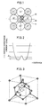
- FIG.1 is a schematic view showing the motion of an impurity atom Li in KCl:Li which is one of the ionic crystal systems.
- a Li+ ion 12 of the substitutional impurity is loosely bound into a vacant space 11 surrounded by K+ ions shown by hatched circles.
- the Li+ ion 12 moves by the tunneling through many stable positions 13 represented by small black circles in the gap 11.
- the quantum energy level due to the unharmonic vibration of the interstitial oxygen impurity is shown in FIG.2.
- the horizontal axis represents a distance between atoms and the vertical axis represents an energy level.
- a curved line is a characteristic line of the unharmonic potential for interstitial impurity oxygen.
- a symbol ⁇ denotes an energy gap between low energy quantum levels. It should be noted that the physical phenomenon causing the low energy excitation due to the interstitial oxygen impurity is considerably different from that in the above mentioned ionic impurity crystals, as described below.
- the oxygen impurity forms the covalent bonds together with two silicon atoms located on both sides thereof.
- a delicate balance between an attracting force and a repulsive force of the inter atomic potential or a kind of the quasi Jahn-Teller effect exists.
- the repulsive force is slightly superior to the attracting force. Therefore, the oxygen impurity becomes located at an off-center position slightly away from the original Si-Si covalent binding axis.
- the interstitial oxygen impurity presents the unharmonic vibrational motion including the rotational motion around a covalent binding axis.
- the occurrence of the low energy excitation or its physical behavior could not be anticipated from the consideration of the above-described ionic crystal or the impurities in metal.
- the low energy excitation is clearly distinct between the ionic crystal and metal systems and the silicon crystal.
- the energy-level spacing ⁇ between the quantum levels in the ionic crystal system or the metal system is approximately 0.1 - 0.3 meV.
- the energy gap between the quantum levels of the interstitial oxygen impurity in the silicon crystal (FIG.2) is one order greater than the former case.
- the inventors of the present invention found that the physical law described previously is applicable to the interstitial oxygen impurity in the silicon crystal.
- the physical law is also applicable to the crystal defects relating to the oxygen impurity producing the unharmonic vibration.
- the related crystal defects either occurs together with the interstitial oxygen impurity or independently thereof.
- a result of the experiment conducted by the present inventors reveals that a temperature dependence of the elastic constant differs greatly between the silicon crystal having the interstitial oxygen impurity and the silicon crystal having no interstitial impurity oxygen. This experimental result described in detail later supports the above-described theoretical consideration regarding the oxygen impurity and/or the related crystal defects in the silicon crystal.
- the low energy quantum level resulting from the rotational unharmonic vibration of the interstitial oxygen impurity in the silicon crystal is approximately ⁇ ⁇ 4 meV and therefore shows a sensitive pressure dependency. Therefore, the present invention is intended to measure an acoustic velocity of an ultrasonic wave penetrating through the silicon crystal and obtain the elastic constant thereof.
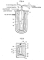
- FIG.4 is a sectional view of a low temperature cryostat.
- a cryostat 15 has three baths 16, 17 and 18.
- the first baths 16 is a vacuum heat insulating bath at a pressure of approximately 10 ⁇ 4 torr at maximum.
- the second bath 17 is a coolant bath in which liquid nitrogen is sealed.
- the third bath 18 is a coolant bath in which a liquid helium is sealed.
- a measuring rod 20 having a sample room 19 positioned at an extreme end thereof is inserted into an central part inside the low temperature cryostat 15.
- wires 21 and 22 extending to an electrical system for generating and detecting an ultrasonic pulse signal
- wires 23 extending to a heat regulator (not shown) for regulating a temperature of the sample room 19, and a code 24 connected to a potentiometer at one end thereof and a thermo couple at the other end.
- a section of an inner part of the sample room 19 is constituted as shown in FIG.5.
- a sample 25 of a silicon crystal (5 mm ⁇ 5 mm of a rectangular cross section, 15 mm in length).
- Ultrasonic pulse transducers 26 and 27 using piezo material are attached to the top and bottom ends of the sample 25, respectively.
- the ultrasonic pulse transducers 26 and 27 are supported and electrically connected to electrodes 30 and 31 by means of brass rods 32 and 33, respectively.
- the wires 21 and 22 shown in FIG.4 are electrically connected to the electrodes 30 and 31, respectively.
- the electrode 31 is supported on a base plate 33 mounted on a bottom plate 34, and the electrode 30 is supported on a base plate 35 which is urged by a coil spring 36.
- a metallic holder 37 surrounds the sample 25 to make the temperature distribution over the sample 25 uniform.
- the holder 37 is not necessarily needed.
- the thermo couple (not shown) for detecting temperature variations of the sample 25 is attached to the metallic holder 37.
- the thermo couple is electrically connected to the code 24 shown in FIG.4.
- a resistance thermometer may be used together with or instead of the thermo couple.
- the above elements are accommodated in a hollow cylindrical solenoid 29.
- a heater wire 38 electrically connected to the heat regulator (not shown) by the wires 23 is wound around the solenoid 29.
- the lowest temperature available in the measuring system described above is around 6K when the cooling medium bath 18 is not kept in a vacuum.
- the lowest temperature of about 2K is available.
- the frequency of the ultrasonic pulse may be set in the range of 100kHz to 1GHz.
- a curved line II is a characteristic line of a silicon crystal including no interstitial oxygen impurity or the related crystal defects.
- the temperature ⁇ /k of silicon crystal is approximately 25K.
- the elastic constant of the silicon crystal including the interstitial oxygen impurity shows an abnormal variation at the temperature around 25K, as compared with the silicon crystal having no interstitial impurity oxygen.
- An amount ⁇ (relative value) of the abnormal variation in the elastic constant (or ultrasonic velocity) is of the order of 10 ⁇ 4.
- a relative accuracy of the measurement of the ultrasonic velocity in the measuring system may be ensured to be of the order of 10 ⁇ 6.
- the concentration (density) of the interstitial oxygen impurity and/or the related crystal defects is substantially proportional to the amount ⁇ of the abnormal variation in elastic constant (or ultrasonic velocity). Therefore, it is possible to obtain the concentration of the interstitial oxygen impurity and/or the related crystal defects by measuring the amount ⁇ of the abnormal variation in elastic constant.
- the present invention makes it possible to obtain the concentration of the interstitial oxygen impurity and/or the related crystal defects in the deeply doped silicon crystal (including donors or acceptors of 0.1 ppm or over) by use of the ultrasonic pulse. It should be appreciated that the present invention measures the concentration of the interstitial oxygen impurity and/or related crystal defects without destroying the crystal. Moreover, the present invention is applicable to not only p-type semiconductor but also n-type semiconductor.
- the present invention is not limited to the embodiments described above, but various variations and modifications may be made without departing from the scope of the present invention.
- the present invention is applicable to semiconductor other than silicon crystal such as GaAs.
Landscapes
- Physics & Mathematics (AREA)
- Biochemistry (AREA)
- Health & Medical Sciences (AREA)
- Life Sciences & Earth Sciences (AREA)
- Chemical & Material Sciences (AREA)
- Analytical Chemistry (AREA)
- General Health & Medical Sciences (AREA)
- General Physics & Mathematics (AREA)
- Immunology (AREA)
- Pathology (AREA)
- Acoustics & Sound (AREA)
- Testing Or Measuring Of Semiconductors Or The Like (AREA)
- Investigating Or Analysing Materials By Optical Means (AREA)
- Investigating Or Analyzing Materials By The Use Of Ultrasonic Waves (AREA)
Applications Claiming Priority (2)
| Application Number | Priority Date | Filing Date | Title |
|---|---|---|---|
| JP314984/86 | 1986-12-26 | ||
| JP61314984A JPS63165754A (ja) | 1986-12-26 | 1986-12-26 | 半導体中の格子欠陥測定方法 |
Publications (3)
| Publication Number | Publication Date |
|---|---|
| EP0273395A2 true EP0273395A2 (de) | 1988-07-06 |
| EP0273395A3 EP0273395A3 (en) | 1990-04-25 |
| EP0273395B1 EP0273395B1 (de) | 1992-12-09 |
Family
ID=18060019
Family Applications (1)
| Application Number | Title | Priority Date | Filing Date |
|---|---|---|---|
| EP87119146A Expired - Lifetime EP0273395B1 (de) | 1986-12-26 | 1987-12-23 | Verfahren zur Messung von Gitterfehlstellen in einem Halbleiter |
Country Status (5)
| Country | Link |
|---|---|
| US (1) | US4803884A (de) |
| EP (1) | EP0273395B1 (de) |
| JP (1) | JPS63165754A (de) |
| KR (1) | KR900005247B1 (de) |
| DE (1) | DE3783022T2 (de) |
Cited By (3)
| Publication number | Priority date | Publication date | Assignee | Title |
|---|---|---|---|---|
| US5210626A (en) * | 1989-09-27 | 1993-05-11 | Canon Kabushiki Kaisha | Head-up display device |
| RU2185607C1 (ru) * | 2001-05-18 | 2002-07-20 | Таганрогский государственный радиотехнический университет | Способ измерения скорости ультразвука в кристаллах |
| EP1997940A4 (de) * | 2006-03-03 | 2010-09-08 | Univ Niigata | Verfahren zur herstellung eines si-einkristallstabs nach dem cz-verfahren |
Families Citing this family (11)
| Publication number | Priority date | Publication date | Assignee | Title |
|---|---|---|---|---|
| US5627320A (en) * | 1988-03-23 | 1997-05-06 | Texas Instruments Incorporated | Apparatus and method for automated non-destructive inspection of integrated circuit packages |
| JPH0651860U (ja) * | 1992-09-08 | 1994-07-15 | ローム株式会社 | 半導体ウエハ弾性係数測定装置 |
| US5469742A (en) * | 1993-03-09 | 1995-11-28 | Lee; Yong J. | Acoustic temperature and film thickness monitor and method |
| US5996415A (en) | 1997-04-30 | 1999-12-07 | Sensys Instruments Corporation | Apparatus and method for characterizing semiconductor wafers during processing |
| US6019000A (en) * | 1997-11-20 | 2000-02-01 | Sensys Instruments Corporation | In-situ measurement of deposition on reactor chamber members |
| US7083327B1 (en) * | 1999-04-06 | 2006-08-01 | Thermal Wave Imaging, Inc. | Method and apparatus for detecting kissing unbond defects |
| US6865948B1 (en) * | 2002-01-29 | 2005-03-15 | Taiwan Semiconductor Manufacturing Company | Method of wafer edge damage inspection |
| DE102006040486A1 (de) * | 2006-08-30 | 2008-03-13 | Wacker Chemie Ag | Verfahren zur zerstörungsfreien Materialprüfung von hochreinem polykristallinen Silicium |
| US8987843B2 (en) | 2012-11-06 | 2015-03-24 | International Business Machines Corporation | Mapping density and temperature of a chip, in situ |
| JP6244833B2 (ja) * | 2013-01-31 | 2017-12-13 | 国立大学法人 新潟大学 | シリコンウェーハ中の原子空孔濃度の絶対値の決定方法 |
| CN114636677A (zh) * | 2020-12-15 | 2022-06-17 | 中国科学院微电子研究所 | 一种半导体缺陷表征的方法、装置、系统、设备及介质 |
Family Cites Families (3)
| Publication number | Priority date | Publication date | Assignee | Title |
|---|---|---|---|---|
| US4342518A (en) * | 1980-12-01 | 1982-08-03 | The United States Of America As Represented By The Secretary Of The Navy | Subseafloor environmental simulator |
| US4366713A (en) * | 1981-03-25 | 1983-01-04 | General Electric Company | Ultrasonic bond testing of semiconductor devices |
| US4621233A (en) * | 1984-01-13 | 1986-11-04 | Rensselaer Polytechnic Institute | Non-destructive testing of semiconductors using acoustic wave method |
-
1986
- 1986-12-26 JP JP61314984A patent/JPS63165754A/ja active Pending
-
1987
- 1987-12-22 US US07/136,691 patent/US4803884A/en not_active Expired - Lifetime
- 1987-12-23 EP EP87119146A patent/EP0273395B1/de not_active Expired - Lifetime
- 1987-12-23 DE DE8787119146T patent/DE3783022T2/de not_active Expired - Fee Related
- 1987-12-24 KR KR1019870014860A patent/KR900005247B1/ko not_active Expired
Cited By (3)
| Publication number | Priority date | Publication date | Assignee | Title |
|---|---|---|---|---|
| US5210626A (en) * | 1989-09-27 | 1993-05-11 | Canon Kabushiki Kaisha | Head-up display device |
| RU2185607C1 (ru) * | 2001-05-18 | 2002-07-20 | Таганрогский государственный радиотехнический университет | Способ измерения скорости ультразвука в кристаллах |
| EP1997940A4 (de) * | 2006-03-03 | 2010-09-08 | Univ Niigata | Verfahren zur herstellung eines si-einkristallstabs nach dem cz-verfahren |
Also Published As
| Publication number | Publication date |
|---|---|
| EP0273395A3 (en) | 1990-04-25 |
| EP0273395B1 (de) | 1992-12-09 |
| KR880008023A (ko) | 1988-08-30 |
| KR900005247B1 (ko) | 1990-07-21 |
| DE3783022T2 (de) | 1993-06-24 |
| JPS63165754A (ja) | 1988-07-09 |
| US4803884A (en) | 1989-02-14 |
| DE3783022D1 (de) | 1993-01-21 |
Similar Documents
| Publication | Publication Date | Title |
|---|---|---|
| EP0273395B1 (de) | Verfahren zur Messung von Gitterfehlstellen in einem Halbleiter | |
| Caswell | Investigation of Low‐Temperature Internal Friction | |
| US4393348A (en) | Method and apparatus for determining minority carrier diffusion length in semiconductors | |
| US6206961B1 (en) | Method of determining oxygen precipitation behavior in a silicon monocrystal | |
| Niblett | Low‐Frequency Measurements on the Bordoni Internal Friction Peak in Copper | |
| Gilbert | A dynamic gravimeter of novel design | |
| Kofstad et al. | Apparatus for continuous recording of internal friction | |
| JPH07174742A (ja) | 結晶欠陥測定方法 | |
| Gorbachuk | Measuring transducers and sensors | |
| US3787694A (en) | Fluidic detector for the detection of radiant energy and for the analysis of gas mixtures | |
| Stokes | Apparatus for the measurement of Young's modulus, between 200 and 700° C by transverse vibration in vacuum | |
| Gerritsen et al. | Problems Arising in the Measurement of Small Magnetic Forces at Low Temperatures by the Faraday Method | |
| Schoening et al. | Use of an elastic model in calculating the X-ray scattering from the interstitial Ti–O solid solution | |
| Lytton et al. | Apparatus for the determination of dynamic Young's modulus and internal friction in vacuum at temperatures from 25° C to 1200° C | |
| Ballaro et al. | Viscosity and light scattering in critical mixtures | |
| Southgate | Measurement of low values of internal friction at elevated temperatures | |
| Firle | Torsional damping in pyrolytic graphite | |
| Schnell et al. | An automatic torsion pendulum for measuring the temperature dependence of internal friction | |
| Watanabe et al. | Lattice parameter and thermal expansion measurements of a LiF (001) surface by He-atom beam diffraction method | |
| Perz et al. | Experimental Determination of Changes in the Fermi Surface of Metallic Tin Produced by Uniaxial Tension | |
| Tietje et al. | Low-temperature elastic experiments on glasses at very low frequencies | |
| JP2614730B2 (ja) | 半導体中の欠陥の測定装置および方法 | |
| Hinton | Measurements of dynamic moduli and internal friction of metals and alloys | |
| Southgate | Dislocation mobility and pinning in hard materials through internal friction studies | |
| Sprungmann et al. | An improved reed pendulum apparatus and techniques for the study of internal friction of ceramic single crystals |
Legal Events
| Date | Code | Title | Description |
|---|---|---|---|
| PUAI | Public reference made under article 153(3) epc to a published international application that has entered the european phase |
Free format text: ORIGINAL CODE: 0009012 |
|
| AK | Designated contracting states |
Kind code of ref document: A2 Designated state(s): DE FR GB |
|
| PUAL | Search report despatched |
Free format text: ORIGINAL CODE: 0009013 |
|
| AK | Designated contracting states |
Kind code of ref document: A3 Designated state(s): DE FR GB |
|
| 17P | Request for examination filed |
Effective date: 19900627 |
|
| 17Q | First examination report despatched |
Effective date: 19910802 |
|
| GRAA | (expected) grant |
Free format text: ORIGINAL CODE: 0009210 |
|
| AK | Designated contracting states |
Kind code of ref document: B1 Designated state(s): DE FR GB |
|
| PGFP | Annual fee paid to national office [announced via postgrant information from national office to epo] |
Ref country code: GB Payment date: 19921209 Year of fee payment: 6 |
|
| PGFP | Annual fee paid to national office [announced via postgrant information from national office to epo] |
Ref country code: FR Payment date: 19921216 Year of fee payment: 6 |
|
| REF | Corresponds to: |
Ref document number: 3783022 Country of ref document: DE Date of ref document: 19930121 |
|
| PGFP | Annual fee paid to national office [announced via postgrant information from national office to epo] |
Ref country code: DE Payment date: 19930226 Year of fee payment: 6 |
|
| ET | Fr: translation filed | ||
| PLBE | No opposition filed within time limit |
Free format text: ORIGINAL CODE: 0009261 |
|
| STAA | Information on the status of an ep patent application or granted ep patent |
Free format text: STATUS: NO OPPOSITION FILED WITHIN TIME LIMIT |
|
| 26N | No opposition filed | ||
| PG25 | Lapsed in a contracting state [announced via postgrant information from national office to epo] |
Ref country code: GB Effective date: 19931223 |
|
| GBPC | Gb: european patent ceased through non-payment of renewal fee |
Effective date: 19931223 |
|
| PG25 | Lapsed in a contracting state [announced via postgrant information from national office to epo] |
Ref country code: FR Effective date: 19940831 |
|
| PG25 | Lapsed in a contracting state [announced via postgrant information from national office to epo] |
Ref country code: DE Effective date: 19940901 |
|
| REG | Reference to a national code |
Ref country code: FR Ref legal event code: ST |