EP0273539A2 - Logische Steuereinrichtung - Google Patents
Logische Steuereinrichtung Download PDFInfo
- Publication number
- EP0273539A2 EP0273539A2 EP87302036A EP87302036A EP0273539A2 EP 0273539 A2 EP0273539 A2 EP 0273539A2 EP 87302036 A EP87302036 A EP 87302036A EP 87302036 A EP87302036 A EP 87302036A EP 0273539 A2 EP0273539 A2 EP 0273539A2
- Authority
- EP
- European Patent Office
- Prior art keywords
- storage means
- bits
- random access
- information
- access storage
- Prior art date
- Legal status (The legal status is an assumption and is not a legal conclusion. Google has not performed a legal analysis and makes no representation as to the accuracy of the status listed.)
- Withdrawn
Links
Images

Classifications
-
- G—PHYSICS
- G05—CONTROLLING; REGULATING
- G05B—CONTROL OR REGULATING SYSTEMS IN GENERAL; FUNCTIONAL ELEMENTS OF SUCH SYSTEMS; MONITORING OR TESTING ARRANGEMENTS FOR SUCH SYSTEMS OR ELEMENTS
- G05B19/00—Program-control systems
- G05B19/02—Program-control systems electric
- G05B19/04—Program control other than numerical control, i.e. in sequence controllers or logic controllers
- G05B19/05—Programmable logic controllers, e.g. simulating logic interconnections of signals according to ladder diagrams or function charts
Definitions
- This invention relates to logic controllers.
- Microprocessors are now being used in relation to control systems for vehicles, security systems and domestic appliances, which traditionally used electromechanical devices. Microprocessors however, have an architecture that is inefficient for use in such control systems, because their binary word-orientated structure is more suited to applications involving numeric operations. It is therefore not effective to use microprocessore in many applications where only simple processing of data is required.
- Microprocessors are also suseptible to crashing due for example to overwriting a stack, because program and data information are stored in the same memory space.
- a logic controller comprising, random access storage means for storing single binary bits of information, programmable read only storage means, an instruction decoder and a timer circuit for measuring a duration of time, the arrangement being such that binary bits of information corresponding to a current "condition" of a number of accessories and to a number of timer “channels", are supplied in a cycle to the random access storage means, the bits being examined by the instruction decoder, in relation to a read only storage means program, to provide output bits of information to control the accessories.
- a shift register is used to write single bits of information to the random access storage means and a shift register is also preferably used to read single bits of information from the random access storage means.
- a counter is used to clock the single bits of information into and out of the random access storage means.
- the timer circuit preferably comprises, a counter, an adder, random access storage means and digital comparison means, the arrangement being such that in one cycle of the counter a duration of time in the form of a binary word is added to the present binary state of the counter, using the adder. The result of the addition is then stored in the random access storage means. In the next cycle the result in the random access storage means is compared with the next binary state of the counter, using the digital comparison means. The process is repeated, every cycle, until the result of the addition is found to be equal to the binary state of the counter in which case the duration of time is measured.
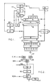
- random access storage means are provided at the core of the controller 1 by a 256 ⁇ 1 bit RAM 2.
- Input signals 3 to the controller 1 come from various accessories (not shown) such as switches and sensors.
- the inputs 3 are clocked into an input shift register 4 in the form of single input bits 5 of information and the shift register 4 is connected so that the input bits 5 are then clocked into the top 6 of the RAM 2, by an incremented counter 7.
- Single outputs bits 8 of information are generated by the controller and are stored at the bottom 9 of the RAM 2.
- the output bits 8 are clocked into an output shift register 10 by a decremented counter 11.
- the output bits 8 are then clocked into a latch 12 which sends output signals 13 to drive accessories (not shown) such as relays and transistor switches.
- Timer information 14 related to an input device is stored in a second RAM 15 as a ten bit word.
- the ten bit word represents a timer channel.
- the first eight bits represent a time and the 9th and 10th bits are control bits.
- Single timer bits 16 of information are generated by a timer circuit 17 comprising essentially a counter 18, an adder 19, and digital comparison means or a comparator 20 for comparing 8 bit words for equality.
- the comparator 20 generates the timer bits 16 which are clocked into the input shift register 4, and then clocked into the top 6 of the RAM 2, together with the input bits 5.
- Programmed instructions 21 for controlling the controller 1 are stored in programmable read only storage means or in a ROM 22.
- the instructions 21 are fed into an instruction decoder 23.
- the instruction decoder 23 is connected so that bits can be read from or written to the RAM 2.
- the controller 1 is synchronised using a clock pulse generator 24.
- An eight bit counter 25 generates an eight bit timer word 26 every 40mS.
- the output of the counter 25 is divided using a divider 27 to generate a further eight bit timer word 28 every 4 seconds.
- the 9th control bit of the timer information 14 is used to select the output from either the counter 25 or the divider 27 using a multiplexer 29.
- the eight bit timer word from the multiplexer 29 is fed into an adder 19 and is added to another eight bit word representing a duration of time 30.
- the output of the adder 19 gives the first eight bits for the timer information 14 which is stored in the second RAM 15. Up to sixteen timer channels in the form of ten bit words may be stored as timer information.
- the first eight bits of the timer information 14 are compared with the current eight bit timer word 26 using the comparater 20.
- the comparater 20 is enabled or inhibited depending upon the state of the 10th control bit of the timer information 14.
- the comparator 20 gives an output 31 if the two inputs are equal and the output 31 sets the appropriate timer bit 16 of the input shift register 4 for that timer channel. This is subsequently clocked into the RAM 2.
- FIG. 3 a program is shown which defines the instructions 21 for controlling the controller 1. Each line number represents an instruction 21.
- the operation of the logic controller 1 is now described, in which the controller controls accesories in a car.
- the input signals 3 are provided by sensors to four doors on the car and by a sensor to the car's ignition.
- An output signal 13 is generated by the controller to turn on a courtesy light in the car, if any door is opened. The light further remains on for 12 seconds once all the doors are closed again. However, the courtesy light is turned off if the ignition is switched on.
- the controller operates in a cycle. Thus, every 40mS the controller 1 monitors the input signals 3 and characterises the ouput signal 13 depending upon the combination of input signals and depending upon a duration of time.
- the five current input bits 5 and timer bits 16, which were set in the previous cycle, are clocked into the RAM 2.
- the 40mS delay allows any switch bounce affecting the input signals 3 to settle down within the 40mS.
- the output bit 8 for the courtesy light is then clocked into the output shift register 10 and then into the latch 12 which sends and output signal 13 to turn on or off the courtesy light.
- the timer circuit operates to set or clear a timer bit 16.
- the programmed instructions 21 next take over control of the controller 1.
- the first part of the program from line numbers 1 to 15, defines the addresses in the RAM for the input bits 5, output bit 8 and timer bit 16.
- the instructions at line numbers 16 to 18 initialize the controller 1 after a power-on reset.
- the input bits 5 from the door are next examined in turn, from line numbers 19 to 22, and if any input bit 5 indicates that a door is open the program counter jumps to line number 24, which sets the output bit 8 to turn on the courtesy light in the next cycle.
- the timer is then started or set, at line number 25, by sending an eight bit word 30, equivalent to 3 cycles of the divider 27, to the adder 19 together with the current eight bit word 28, which is selected from the divider 27.
- the result is stored in the first eight bits of the second RAM 15, in this case at address one (line number 11). Whenever a door is open the timer is therefore always set in that cycle.
- the program counter jumps to the same point in the program that occurs next if any door is found to be open, at line number 26, skipping the instruction to set the timer. At this point the timer is tested to see if the stored timer information 14 equals the present eight bit word 28 from the divider 27 by testing the timer bit 16. A match would occur in this case after 300 cycles, or 12 seconds from the cycle in which the timer was set. If a match occurs the output bit 8 is cleared, at line number 27, to turn off the courtesy light in the next cycle, and the timer channel is inhibited, at line number 28, by clearing the 10th bit of the timer information 14. If a match does not occur the program counter jumps to a point in the program that occurs next if a match does occur, at line number 30.
- the input bit 5 relating to the ignition is tested so that if the ignition is 'on', the output bit 8 is cleared to turn off the light, and the timer channel is again inhibited, at line number 32, and the program finishes. If the ignition is 'off' the program counter jumps to the end of the program, at line number 34. The program counter enters an infinite loop until the end of the 40mS cycle. The process is then repeated.
- the cyclic mode of operation has the additional advantage that it excludes the requirement for extra watchdog hardware or software, to ensure that the controller is operating correctly.
- a convenient logic controller is provided for processing single bits of information, such as is provided by switches and sensors from various devices.
- logic controller is designed so that expansion may be easily carried out. There is also space in the RAM for remembering previous events.
Landscapes
- Physics & Mathematics (AREA)
- General Physics & Mathematics (AREA)
- Engineering & Computer Science (AREA)
- Automation & Control Theory (AREA)
- Programmable Controllers (AREA)
Applications Claiming Priority (2)
| Application Number | Priority Date | Filing Date | Title |
|---|---|---|---|
| GB8629522A GB2198864B (en) | 1986-12-10 | 1986-12-10 | Logic controller |
| GB8629522 | 1986-12-10 |
Publications (2)
| Publication Number | Publication Date |
|---|---|
| EP0273539A2 true EP0273539A2 (de) | 1988-07-06 |
| EP0273539A3 EP0273539A3 (de) | 1989-11-02 |
Family
ID=10608775
Family Applications (1)
| Application Number | Title | Priority Date | Filing Date |
|---|---|---|---|
| EP87302036A Withdrawn EP0273539A3 (de) | 1986-12-10 | 1987-03-10 | Logische Steuereinrichtung |
Country Status (4)
| Country | Link |
|---|---|
| EP (1) | EP0273539A3 (de) |
| JP (1) | JPS63191203A (de) |
| DE (1) | DE273539T1 (de) |
| GB (1) | GB2198864B (de) |
Cited By (1)
| Publication number | Priority date | Publication date | Assignee | Title |
|---|---|---|---|---|
| EP0400820A3 (de) * | 1989-05-31 | 1992-08-05 | STMicroelectronics, Inc. | Inhaltsadressierbarer Speicher |
Family Cites Families (4)
| Publication number | Priority date | Publication date | Assignee | Title |
|---|---|---|---|---|
| US4058850A (en) * | 1974-08-12 | 1977-11-15 | Xerox Corporation | Programmable controller |
| US4266281A (en) * | 1979-04-02 | 1981-05-05 | Allen-Bradley Company | Microprogrammed programmable controller |
| EP0112427B1 (de) * | 1982-12-28 | 1988-09-21 | International Business Machines Corporation | Programmierbare logische Steuereinrichtung |
| JPS61239491A (ja) * | 1985-04-13 | 1986-10-24 | Fujitsu Ltd | 電子装置 |
-
1986
- 1986-12-10 GB GB8629522A patent/GB2198864B/en not_active Expired - Lifetime
-
1987
- 1987-03-10 EP EP87302036A patent/EP0273539A3/de not_active Withdrawn
- 1987-03-10 DE DE1987302036 patent/DE273539T1/de active Pending
- 1987-12-09 JP JP31180587A patent/JPS63191203A/ja active Pending
Cited By (2)
| Publication number | Priority date | Publication date | Assignee | Title |
|---|---|---|---|---|
| EP0400820A3 (de) * | 1989-05-31 | 1992-08-05 | STMicroelectronics, Inc. | Inhaltsadressierbarer Speicher |
| US5363499A (en) * | 1989-05-31 | 1994-11-08 | Sgs-Thomson Microelectronics, Inc. | Cam for outputting control signals of action fields in response to matches of inputting digital timer signals with data in comparing fields |
Also Published As
| Publication number | Publication date |
|---|---|
| GB2198864B (en) | 1990-11-21 |
| DE273539T1 (de) | 1989-01-05 |
| GB8629522D0 (en) | 1987-01-21 |
| GB2198864A (en) | 1988-06-22 |
| EP0273539A3 (de) | 1989-11-02 |
| JPS63191203A (ja) | 1988-08-08 |
Similar Documents
| Publication | Publication Date | Title |
|---|---|---|
| US4392133A (en) | Electronic lock with changeable opening code | |
| US3470542A (en) | Modular system design | |
| US5062109A (en) | Memory tester | |
| US4785416A (en) | Microprocessor timing emulator having a "Wait" state | |
| US4752928A (en) | Transaction analyzer | |
| JPH0635993B2 (ja) | デ−タ取込み装置 | |
| EP0273539A2 (de) | Logische Steuereinrichtung | |
| US4675843A (en) | Programmable logic controller | |
| US4393469A (en) | Process control apparatus | |
| JPS6114524B2 (de) | ||
| US4538923A (en) | Test circuit for watch LSI | |
| US5875197A (en) | Addressable serial test system | |
| AU592882B2 (en) | Apparatus for detecting sequential data string | |
| EP0662691B1 (de) | Zähleinheit für nichtflüchtige Speicher | |
| AU643512B2 (en) | A sequencer for generating binary output signals | |
| JPH0731611B2 (ja) | 装置動作モ−ド切替回路 | |
| SU1681320A1 (ru) | Устройство задани программы обучени | |
| US5644309A (en) | Digital comonent testing apparatus and method | |
| SU1714645A1 (ru) | Устройство управлени тренажером операторов | |
| SU1094046A1 (ru) | Устройство дл управлени тренажером операторов систем управлени | |
| SU1762298A1 (ru) | Программное временное устройство | |
| SU1608673A1 (ru) | Устройство дл отладки программ | |
| SU1439535A1 (ru) | Устройство дл программного управлени | |
| SU1580542A1 (ru) | Формирователь импульсов | |
| SU1397863A1 (ru) | Устройство воспроизведени измен ющегос магнитного пол |
Legal Events
| Date | Code | Title | Description |
|---|---|---|---|
| PUAI | Public reference made under article 153(3) epc to a published international application that has entered the european phase |
Free format text: ORIGINAL CODE: 0009012 |
|
| AK | Designated contracting states |
Kind code of ref document: A2 Designated state(s): AT BE CH DE ES FR GB GR IT LI LU NL SE |
|
| EL | Fr: translation of claims filed | ||
| DET | De: translation of patent claims | ||
| PUAL | Search report despatched |
Free format text: ORIGINAL CODE: 0009013 |
|
| AK | Designated contracting states |
Kind code of ref document: A3 Designated state(s): AT BE CH DE ES FR GB GR IT LI LU NL SE |
|
| 17P | Request for examination filed |
Effective date: 19900411 |
|
| 17Q | First examination report despatched |
Effective date: 19920324 |
|
| STAA | Information on the status of an ep patent application or granted ep patent |
Free format text: STATUS: THE APPLICATION IS DEEMED TO BE WITHDRAWN |
|
| 18D | Application deemed to be withdrawn |
Effective date: 19940305 |
|
| RIN1 | Information on inventor provided before grant (corrected) |
Inventor name: MOON, ANTHONY GEORGE |