EP0273638A2 - Systèmes d'analyse d'images - Google Patents
Systèmes d'analyse d'images Download PDFInfo
- Publication number
- EP0273638A2 EP0273638A2 EP87311044A EP87311044A EP0273638A2 EP 0273638 A2 EP0273638 A2 EP 0273638A2 EP 87311044 A EP87311044 A EP 87311044A EP 87311044 A EP87311044 A EP 87311044A EP 0273638 A2 EP0273638 A2 EP 0273638A2
- Authority
- EP
- European Patent Office
- Prior art keywords
- row
- sensors
- charge
- sensor
- storage means
- Prior art date
- Legal status (The legal status is an assumption and is not a legal conclusion. Google has not performed a legal analysis and makes no representation as to the accuracy of the status listed.)
- Granted
Links
Images

Classifications
-
- H—ELECTRICITY
- H04—ELECTRIC COMMUNICATION TECHNIQUE
- H04N—PICTORIAL COMMUNICATION, e.g. TELEVISION
- H04N1/00—Scanning, transmission or reproduction of documents or the like, e.g. facsimile transmission; Details thereof
- H04N1/46—Colour picture communication systems
- H04N1/48—Picture signal generators
- H04N1/486—Picture signal generators with separate detectors, each detector being used for one specific colour component
Definitions
- the present invention relates primarily to a raster input scanning device, and more particularly to raster input scanners having color sensor arrays for deriving color information from a scanned image.
- Raster input scanning devices generally include an array of photoelectric sensors or detectors or photosites arranged across an image-scanning field for detecting light from an image; a data transmission and processing system for taking the image data derived from the photoelectric detectors and passing the image information to a data processing system, such as a microprocessor; and a transport for relative movement of the image to be scanned across the scanning field so that photoelectric sensors extending transversely across the image field direction of motion are able to detect, on a line-by-line basis, the images on the scanned surface.
- a data processing system such as a microprocessor
- a transport for relative movement of the image to be scanned across the scanning field so that photoelectric sensors extending transversely across the image field direction of motion are able to detect, on a line-by-line basis, the images on the scanned surface.
- a data processing system such as a microprocessor
- a transport for relative movement of the image to be scanned across the scanning field so that photoelectric sensors extending transversely across
- each scanning operation produced selected color information based on the filter over the image.
- the detectors are able to detect only the difference between a light and dark image, and may use detectors similar to those detecting only black and white information.
- a commercial product by Toshiba Corporation, Model No. TCD 112 provides a sensor arrangement including a plurality of arrays in offset and overlapping relationship to cover the X-direction of an image field. This product splits each individual photosite into three sites, each with a color filter. Color image information may be derived from the sensors, and is passed in sequential fashion to a data processor. It would be preferable, however, to provide an array with larger photosites since a larger photosite is more sensitive to the light focused thereon and allows the document to be scanned at a higher rate. Additionally, the overlapping and offset arrangement of the TCD 112 makes it difficult to align the segments. Thus, extensive processing of the signal is required to compensate for the offset alignment of the arrays.
- the primary object of the present invention is to provide a new photosite sensor array arrangement suitable for use in a color image raster input scanning system.
- the present invention provides, a scanner system which is claimed in the appended claims.
- the invention provides for an array extending across the entire image field detecting the entire X-direction of an image to be scanned so that no alignment of the arrays is required in this respect.
- Large photosites may be used in each row, as a single row of photosites detects only a particular light wavelength, while succeeding similar rows detect other wavelengths.
- the available array space does not need to be divided for the purpose of providing color photosites on a single array.
- This arrangement maintains the sensitivity of the array at a high level, and allows shorter integration times to be utilized, thereby increasing the speed of image reading.
- FIGURE 1 shows, somewhat schematically, an arrangement for an optical system of a raster input scanner of the present invention, and providing an image from an original document 8 supported on platen 9 to be scanned by an imaging sensor array A.
- the optical system of raster input scanner 10 comprises lamp 12 and adjustable reflector 14 for illuminating document 8.
- Mirrors 16, 18, 20 and 22 direct light reflected from the document 8 to a lens 24 to focus and direct the image on the sensor array A.
- Information derived from the sensors will be directed to a conventional information or data-processing system (not shown). The acquired data will be manipulated as desired for display, storage, etc. It will be appreciated that the present invention is readily applicable to other arrangements.
- Fiber optic assemblies may be used to direct an image to the array. Additionally, it will be appreciated that while the described embodiment scans reflected light, the invention is equally applicable to other optical storage media such as slides, transparencies, aperture cards, etc. Also not shown is a carriage means for moving the document 8 in a longitudinal (Y) direction (left-to-right as viewed in FIGURE 1) to provide scan lines moving successively along the document 8 to be scanned by the sensor array.
- Y longitudinal
- the elements comprising the mechanical and optical systems in a raster input scanner are widely varying and well known in the art, and do not form a part of the present invention.
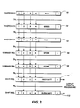
- sensor array A is comprised of at least three parallel rows of sensors comprising photosites 100, 102, 104, best shown in FIGURE 2.
- photosites 100, 102, 104 an increase in the number of photosites results in improved image resolution.
- a photosite row may include upwards of 3500 individual photosites.
- a limited number of photosites, labeled 1, 2, 3, 4 and n is shown as an example.
- FIGURE 2 shows an arrangement including photosite rows 100, 102, 104 arranged to pass information derived from the image to storage means comprising storage registers 106, 108, and from the storage registers 106, 108 to shift registers 110, 112, from which information may be passed to a data-processing system (not shown). All three photosite rows, 100, 102, 104, as well as the storage registers 106, 108 and shift registers 110, 112, may be provided on a single monolithic chip to form sensor array A. The rows are arranged perpendicularly to the fast scan (Y-axis) direction of image scanning, which is indicated as the vertical direction in FIGURE 2.
- Y-axis fast scan
- Photosite rows 100, 102, 104 may be comprised of either photodiodes or charge-coupled devices (CCD's). Color filters selected to filter undesired wavelengths of light are arranged over each row of photosites or each photosite.
- photosite rows 102, 104 may be comprised of CCD's,and provided with filters for passing green and red light. Photodiodes often have a better spectral response in the blue light region than CCD's, but do not allow image information to be easily passed through the photosite.
- photosite row 100 may be comprised of photodiodes and located in the array A furthest away from shift registers 110, 112, so that there will be no requirement that image information pass through such sites, thereby allowing the superior response characteristics of the photodiodes for shorter wavelength to be utilized. It will be appreciated that while these colors have been selected for a preferred embodiment, other color combinations of sensors are possible, and within the scope of the present invention. It is also within the scope of the invention to provide that all of the photosites be comprised of CCD's, rather than mixing types.
- Each photosite in photosite rows 100, 102 is connected to a corresponding photosite in a succeeding row, while each photosite in photosite row 104 is connected to a bit in storage register 106 in information-transferring relationship, which is in turn connected to storage register 108.
- storage register 108 passes data from alternating bits to either shift register 110, or through shift register 110 to shift register 112 for transmission of the data to the data processor. The transmission of data by two shift registers serves to increase the rate at which image information may be passed to the data processor.
- photosite row 100 is connected to photosite row 102 through transfer gates TR1
- photosite row 102 is connected to photosite row 104 through transfer gates TR2
- photosite row 104 is connected to storage register 106 through transfer gates TR3
- storage register 106 is connected to storage register 108 transfer gate TR4
- storage register 108 is connected to shift register 110 through TR5
- shift register 110 is connected to shift register 112 through TR6.
- Charge passes between the rows, through the gates, when a positive-going voltage signal triggers the gates TR n to a charge passing condition.
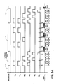
- FIGURE 2A shows the operation of array A in FIGURE 2 with respect to time (t).
- the line labeled INTEGRATE represents successive integration periods or scan times S n of the scanning device over time (t), or the period between times of data transfer.
- a desirable scan time S1 may be approximately 1/300 sec. or approximately the reciprocal of the desired number of scan lines per second.
- photosites in array A are exposed to a selected scan line and store image information or data therefrom as a charge developed at the photosite.
- data derived at each photosite in each photosite row will be passed to a corresponding photosite in a succeeding row.
- Figure 2A shows approximate relative times for transferring or shifting data from photosite row to photosite row, from photosite row to storage register, from the storage register to storage register, from storage register to shift register, or from shift register to shift register by indicating the relative times at which transfer gates TR1, TR2, TR3, TR4, TR5 and TR6 are opened.
- data are passed through successive positions in the array, until the data derived thereby have been moved to the storage and shift registers, whereupon a new scan time S2 is commenced, and the process repeated. With each successive shift, color image data derived from a particular row are moved to succeeding rows until the photosite rows are empty and a new integration period started.
- the sensors may continuously sense light reflected from the image to be sensed, but the amount of light received between integration periods, or during data shifting, is relatively small in comparison to the light detected during the defined integration periods, and has little effect on the output image.
- image data derived at each photosite is transferred or shifted to a corresponding photosite in a succeeding photosite row or bit in a storage register.
- a voltage signal is directed to transfer gates TR6, TR5, TR4, and TR3 at a time t0 as indicated by the substantially simultaneous signals indicated for each in the graphs TR6, TR5, TR4, and TR3 in FIGURE 2A.
- the signal to each of the transfer gates between red-detecting photosite row 104 and the shift registers 110 and 112 allows charge data derived at photosites in red-detecting photosite row 104 to pass to shift registers 110 and 112.
- transfer gates of the set are successively closed, or a non-charge passing condition is created, as data pass therethrough, beginning with transfer gate TR3 and moving in the charge- passing direction towards transfer gate TR6.
- the set of gates TR6, TR5, TR4, and TR3 are simultaneously opened to allow the flow of information derived at red-detecting photosites in row 104 to shift registers 110 and 112.
- gate TR3 is closed to prevent the back flow of charge thereto, trapping charge in the storage registers and shift registers.
- TR4 is closed and the charge remains in only storage register 108 and the two shift registers.
- the green-image information derived at photosite row 102 may be moved in a similar manner to storage register.
- a signal is directed to the set of transfer gates TR4, TR3 and TR2 to open those gates for passage of the green-image information derived at photosite row 102 to storage register 108.
- the gates are sequentially closed.
- gate TR2 is closed to prevent the back flow of charge thereto, trapping charge in the photosite row 104 and the storage registers.
- TR3 is closed and the charge remains in only storage register 108.
- image information must be shifted out to the data-processing section.
- data originally derived at red-detecting photosite row 104 is passed from shift registers 110 and 112, as indicated on the SHIFT REGISTER line of FIGURE 2A to the data processing system within the time described RED SHIFT.
- the shift operation takes a relatively long period of time, for example, on the order of 1000 ⁇ seconds and comprises the longest period during the data movement operation.
- storage register 108 On completion of the transfer of data from storage register 108 to shift registers 110 and 112, storage register 108 is empty, and data from storage register 106, originally derived at blue light detecting photosite row 100, are transferred to storage register 108. Accordingly, at t5, transfer gate TR4 is opened for a predetermined period to allow the transfer of data to storage register 108. At t6 the data in shift registers 110 and 112 are transferred out from the array.
- the data originally derived at blue light detecting photosite row 100 are transferred from storage register 108 to shift registers 110 and 112, in the same manner as previously described, whereby a voltage signal is applied to TR5 and TR6 at t7 to open these transfer gates and allow the transfer of the data from storage register 108 to the shift registers 110 and 112.
- the gates are closed after a predetermined time to prevent the backflow of the charge from the shift registers to the storage registers.
- the data in shift registers 110 and 112 are moved out from the array to, for example, a data-processing stage of the device.
- the transfer process may begin again, with the transfer of data derived at red light detecting photosite row 104 to shift registers 110 and 112.
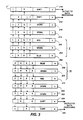
- an array A ⁇ includes the array A as shown in FIGURE 2, and a mirror image of that array offset by half-pixel width.
- the increased number of photosites increases resolution since it provides more photosites per unit of area, and allows a shorter integration period because the period required for integration is dependent on the amount of light detected.
- photosite rows 200, 202, 204, 206, 208, 210 are provided in two groups I and II of three rows each.
- Photosite rows 200, 202, 204 are provided with associated storage registers 212, 214, and shift registers 216, 218, while photosite rows 206, 208, 210 are provided with associated storage registers 220, 222, and shift registers 224, 226.
- the photosite rows are arranged generally as discussed for the arrangement in FIGURE 2.
- Each group of three rows of photosites includes photosite rows suitable for detection of blue, red and green light.
- the blue photosite rows may be comprised of photodiodes.
- a row of photodiodes When a row of photodiodes is used for the blue photosites, they are located in the respective groups furthest from the storage registers so that data are not passed through them, but rather are passed only out from them.
- Each corresponding row of photosites e.g. the two blue rows of photosites, are offset from each other about approximately half photosite width to provide the corresponding photosites in an overlapping arrangement, whereby the image area is covered by two photosites.
Landscapes
- Engineering & Computer Science (AREA)
- Multimedia (AREA)
- Signal Processing (AREA)
- Facsimile Heads (AREA)
- Facsimile Scanning Arrangements (AREA)
Applications Claiming Priority (2)
| Application Number | Priority Date | Filing Date | Title |
|---|---|---|---|
| US06/943,337 US4761683A (en) | 1986-12-18 | 1986-12-18 | Charge transfer in multiple sensor row arrays |
| US943337 | 1992-09-16 |
Publications (3)
| Publication Number | Publication Date |
|---|---|
| EP0273638A2 true EP0273638A2 (fr) | 1988-07-06 |
| EP0273638A3 EP0273638A3 (en) | 1990-05-23 |
| EP0273638B1 EP0273638B1 (fr) | 1993-10-27 |
Family
ID=25479479
Family Applications (1)
| Application Number | Title | Priority Date | Filing Date |
|---|---|---|---|
| EP87311044A Expired - Lifetime EP0273638B1 (fr) | 1986-12-18 | 1987-12-15 | Systèmes d'analyse d'images |
Country Status (4)
| Country | Link |
|---|---|
| US (1) | US4761683A (fr) |
| EP (1) | EP0273638B1 (fr) |
| JP (1) | JPH0734570B2 (fr) |
| DE (1) | DE3787963T2 (fr) |
Families Citing this family (12)
| Publication number | Priority date | Publication date | Assignee | Title |
|---|---|---|---|---|
| GB8824340D0 (en) * | 1988-10-18 | 1988-11-23 | Xerox Corp | Colour detection/recognition apparatus |
| US5196939A (en) * | 1989-12-28 | 1993-03-23 | Loral Fairchild Corporation | Method and apparatus for transferring images from an imaging array |
| US5031032A (en) * | 1990-03-30 | 1991-07-09 | Xerox Corporation | Color array for use in fabricating full width arrays |
| US5119181A (en) * | 1990-03-30 | 1992-06-02 | Xerox Corporation | Color array for use in fabricating full width arrays |
| US5103322A (en) * | 1990-05-14 | 1992-04-07 | Polaroid Corporation | Scanner with retractable roller feed |
| US5148268A (en) * | 1991-04-26 | 1992-09-15 | Xerox Corporation | Multiplexing arrangement for controlling data produced by a color images sensor array |
| EP0522526B1 (fr) * | 1991-07-10 | 1999-04-28 | Sony Corporation | Capteur linéaire de couleur |
| JP2909789B2 (ja) * | 1992-03-13 | 1999-06-23 | 華隆微電子股▼ふん▲有限会司 | 線形カラー電荷結合素子イメージセンサ及びその電荷転送方法 |
| KR950008698B1 (ko) * | 1992-06-09 | 1995-08-04 | 현대전자산업 주식회사 | 반도체소자의 필드산화막 형성방법 |
| US5345319A (en) * | 1993-11-19 | 1994-09-06 | Goldstar Electron Co., Ltd. | Linear color charge coupled device for image sensor and method of driving the same |
| JP2907058B2 (ja) * | 1995-04-21 | 1999-06-21 | 富士ゼロックス株式会社 | 蓄積手段を持つイメージセンサ及び画像読取装置 |
| JP2008230214A (ja) * | 2007-02-19 | 2008-10-02 | Seiko Epson Corp | 流体導出部のシール構造体及びシール方法並びに流体収容容器、再充填流体収容容器及びその再充填方法 |
Family Cites Families (14)
| Publication number | Priority date | Publication date | Assignee | Title |
|---|---|---|---|---|
| US3940602A (en) * | 1974-09-23 | 1976-02-24 | The United States Of America As Represented By The Secretary Of The Navy | Signal processing imager array using charge transfer concepts |
| DE2715097A1 (de) * | 1977-04-04 | 1978-10-12 | Bosch Gmbh Robert | Farbfernsehaufnahmeverfahren |
| DE2838098A1 (de) * | 1978-08-31 | 1980-03-13 | Siemens Ag | Anordnung zur farbbildabtastung |
| DE2838099A1 (de) * | 1978-08-31 | 1980-03-13 | Siemens Ag | Anordnung zur farbbildabtastung |
| US4264921A (en) * | 1979-06-29 | 1981-04-28 | International Business Machines Corporation | Apparatus for color or panchromatic imaging |
| DE2939518A1 (de) * | 1979-09-28 | 1981-04-16 | Siemens AG, 1000 Berlin und 8000 München | Monolithisch integrierte schaltung zur zeilenweisen bildabtastung |
| JPS5651184A (en) * | 1979-10-03 | 1981-05-08 | Hitachi Ltd | Color solid image pickup device |
| CA1175360A (fr) * | 1980-07-03 | 1984-10-02 | Xerox Corporation | Groupe detecteur de signaux couleur |
| US4438457A (en) * | 1981-07-20 | 1984-03-20 | Xerox Corporation | High resolution imager employing staggered sensor structure |
| EP0070620A3 (fr) * | 1981-07-20 | 1985-11-06 | Xerox Corporation | Dispositif de formation d'image à haute densité |
| US4432017A (en) * | 1981-07-20 | 1984-02-14 | Xerox Corporation | Adjacent bilinear photosite imager |
| US4396950A (en) * | 1982-02-26 | 1983-08-02 | Honeywell Inc. | CCD Camera |
| JPS60204170A (ja) * | 1984-03-29 | 1985-10-15 | Toshiba Corp | 画像読取り装置 |
| JPH0665230B2 (ja) * | 1985-12-23 | 1994-08-22 | 株式会社東芝 | 固体撮像装置 |
-
1986
- 1986-12-18 US US06/943,337 patent/US4761683A/en not_active Expired - Fee Related
-
1987
- 1987-12-07 JP JP62309356A patent/JPH0734570B2/ja not_active Expired - Lifetime
- 1987-12-15 EP EP87311044A patent/EP0273638B1/fr not_active Expired - Lifetime
- 1987-12-15 DE DE3787963T patent/DE3787963T2/de not_active Expired - Fee Related
Also Published As
| Publication number | Publication date |
|---|---|
| EP0273638A3 (en) | 1990-05-23 |
| EP0273638B1 (fr) | 1993-10-27 |
| JPH0734570B2 (ja) | 1995-04-12 |
| US4761683A (en) | 1988-08-02 |
| JPS63191467A (ja) | 1988-08-08 |
| DE3787963D1 (de) | 1993-12-02 |
| DE3787963T2 (de) | 1994-05-19 |
Similar Documents
| Publication | Publication Date | Title |
|---|---|---|
| CA1136275A (fr) | Scanner a grande resolution a ensemble bidimensionnel de detecteurs | |
| US5070414A (en) | Method and apparatus for reading image information formed on material | |
| JP2004112611A (ja) | 画像読取装置 | |
| EP0273638B1 (fr) | Systèmes d'analyse d'images | |
| US6437335B1 (en) | High speed scanner using multiple sensing devices | |
| CA1175360A (fr) | Groupe detecteur de signaux couleur | |
| CA1235792A (fr) | Systeme reprographique a balayage electronique des images avec correction des couleurs par matricage | |
| US6593968B1 (en) | Linear image sensor, image reading device, and charge transfer method | |
| US7471327B2 (en) | Image sensor array with variable resolution and high-speed output | |
| EP1471726B1 (fr) | Matrice de capteur d'image | |
| US4754153A (en) | Operating radiation sensors to avoid transfer loss | |
| US6900427B2 (en) | Photosensor assembly with shared charge transfer registers and electronic shutters | |
| US6765699B1 (en) | Photosensor array with decreased scan time for decreased optical sampling rates | |
| US7345793B2 (en) | Scan method | |
| US7656448B2 (en) | System for selecting a format for control data in an imaging device | |
| US7605958B2 (en) | Design parameters for a multi-row linear photosensor array | |
| JPS58173962A (ja) | カラ−原稿読取装置 | |
| JPH01314063A (ja) | 固体撮像装置 | |
| JPH11146134A (ja) | 固体撮像素子 | |
| JPH0562502B2 (fr) | ||
| JP2005276856A (ja) | エリアセンサおよびこれを用いた画像読取装置 | |
| JPH0946489A (ja) | 画像読み取り装置 | |
| JPH07106539A (ja) | 一次元カラーイメージセンサ | |
| JPS632457A (ja) | 画像読取装置 | |
| JPH09116687A (ja) | イメージセンサ及びこれを用いた画像読取装置 |
Legal Events
| Date | Code | Title | Description |
|---|---|---|---|
| PUAI | Public reference made under article 153(3) epc to a published international application that has entered the european phase |
Free format text: ORIGINAL CODE: 0009012 |
|
| AK | Designated contracting states |
Kind code of ref document: A2 Designated state(s): DE GB IT |
|
| PUAL | Search report despatched |
Free format text: ORIGINAL CODE: 0009013 |
|
| AK | Designated contracting states |
Kind code of ref document: A3 Designated state(s): DE GB IT |
|
| 17P | Request for examination filed |
Effective date: 19901115 |
|
| 17Q | First examination report despatched |
Effective date: 19920601 |
|
| GRAA | (expected) grant |
Free format text: ORIGINAL CODE: 0009210 |
|
| AK | Designated contracting states |
Kind code of ref document: B1 Designated state(s): DE GB IT |
|
| REF | Corresponds to: |
Ref document number: 3787963 Country of ref document: DE Date of ref document: 19931202 |
|
| ITF | It: translation for a ep patent filed | ||
| PLBE | No opposition filed within time limit |
Free format text: ORIGINAL CODE: 0009261 |
|
| STAA | Information on the status of an ep patent application or granted ep patent |
Free format text: STATUS: NO OPPOSITION FILED WITHIN TIME LIMIT |
|
| PGFP | Annual fee paid to national office [announced via postgrant information from national office to epo] |
Ref country code: GB Payment date: 19940915 Year of fee payment: 8 Ref country code: DE Payment date: 19940915 Year of fee payment: 8 |
|
| 26N | No opposition filed | ||
| PG25 | Lapsed in a contracting state [announced via postgrant information from national office to epo] |
Ref country code: GB Effective date: 19951215 |
|
| GBPC | Gb: european patent ceased through non-payment of renewal fee |
Effective date: 19951215 |
|
| PG25 | Lapsed in a contracting state [announced via postgrant information from national office to epo] |
Ref country code: DE Effective date: 19960903 |
|
| PG25 | Lapsed in a contracting state [announced via postgrant information from national office to epo] |
Ref country code: IT Free format text: LAPSE BECAUSE OF NON-PAYMENT OF DUE FEES;WARNING: LAPSES OF ITALIAN PATENTS WITH EFFECTIVE DATE BEFORE 2007 MAY HAVE OCCURRED AT ANY TIME BEFORE 2007. THE CORRECT EFFECTIVE DATE MAY BE DIFFERENT FROM THE ONE RECORDED. Effective date: 20051215 |