EP0274199A2 - Couplage entre fibres optiques et guides d'ondes optiques - Google Patents
Couplage entre fibres optiques et guides d'ondes optiques Download PDFInfo
- Publication number
- EP0274199A2 EP0274199A2 EP87309916A EP87309916A EP0274199A2 EP 0274199 A2 EP0274199 A2 EP 0274199A2 EP 87309916 A EP87309916 A EP 87309916A EP 87309916 A EP87309916 A EP 87309916A EP 0274199 A2 EP0274199 A2 EP 0274199A2
- Authority
- EP
- European Patent Office
- Prior art keywords
- optical
- optical fibre
- fibres
- fibre
- exposed
- Prior art date
- Legal status (The legal status is an assumption and is not a legal conclusion. Google has not performed a legal analysis and makes no representation as to the accuracy of the status listed.)
- Granted
Links
Images

Classifications
-
- G—PHYSICS
- G02—OPTICS
- G02B—OPTICAL ELEMENTS, SYSTEMS OR APPARATUS
- G02B6/00—Light guides; Structural details of arrangements comprising light guides and other optical elements, e.g. couplings
- G02B6/24—Coupling light guides
- G02B6/42—Coupling light guides with opto-electronic elements
- G02B6/4201—Packages, e.g. shape, construction, internal or external details
- G02B6/4204—Packages, e.g. shape, construction, internal or external details the coupling comprising intermediate optical elements, e.g. lenses, holograms
- G02B6/4212—Packages, e.g. shape, construction, internal or external details the coupling comprising intermediate optical elements, e.g. lenses, holograms the intermediate optical element being a coupling medium interposed therebetween, e.g. epoxy resin, refractive index matching material, index grease, matching liquid or gel
-
- G—PHYSICS
- G02—OPTICS
- G02B—OPTICAL ELEMENTS, SYSTEMS OR APPARATUS
- G02B6/00—Light guides; Structural details of arrangements comprising light guides and other optical elements, e.g. couplings
- G02B6/24—Coupling light guides
- G02B6/26—Optical coupling means
- G02B6/30—Optical coupling means for use between fibre and thin-film device
-
- G—PHYSICS
- G02—OPTICS
- G02B—OPTICAL ELEMENTS, SYSTEMS OR APPARATUS
- G02B6/00—Light guides; Structural details of arrangements comprising light guides and other optical elements, e.g. couplings
- G02B6/24—Coupling light guides
- G02B6/36—Mechanical coupling means
- G02B6/38—Mechanical coupling means having fibre to fibre mating means
- G02B6/3801—Permanent connections, i.e. wherein fibres are kept aligned by mechanical means
- G02B6/3803—Adjustment or alignment devices for alignment prior to splicing
Definitions
- This invention relates to the jointing of a plurality of optical fibres, such as the optical fibres of an optical fibre ribbon, to optical waveguides of an optical component of the kind comprising a substrate supporting a plurality of optical waveguides.
- the invention is especially, but not exclusively, concerned with the jointing of a plurality of optical fibres to the optical waveguides of an optical component of the aforesaid kind generally referred to as an integrated optic device or an integrated optic chip.
- the improved method comprises the steps of positioning the optical component to one side of a jointing station with end faces of the optical waveguides of the component exposed at the side face of the substrate nearer the jointing station; stripping any protective covering from an end portion of each length of optical fibre to provide exposed end portions of the optical fibres; preparing the end faces of the exposed end portions of the optical fibres so that the end face of each optical fibre is substantially smooth; arranging the exposed end portions of the optical fibres in approximately axial alignment with the optical waveguides; so clamping the exposed end portions of the optical fibres that the exposed end portion of each optical fibre can be caused to move lengthwise to a limited extent relative to the exposed end portions of the other optical fibres; arranging the exposed end portions of the optical fibres, over a limited length between the position at which they are so clamped and the cut back ends of the plurality of optical fibres, to follow a curved path whose centres of curvature lie on a line extending transversely of said optical fibres; causing the exposed end portion of an
- the side face of the optical component in which the end faces of the optical waveguides are exposed has integral therewith or permanently connected thereto beneath the exposed end faces of the optical waveguides a supporting body and the end of the exposed portion of said optical fibre is so permamently connected to the supporting body by curable adhesive that said optical fibre is indirectly permanently connected to the optical component in axial alignment with the corresponding optical waveguide.
- the said optical fibre in effecting accurate axial alignment of the core of said optical fibre and the corresponding optical waveguide, preferably after the exposed end portion of said optical fibre has been so straightened, the said optical fibre is fixed and the position of the optical component with respect to said fixed optical fibre is adjusted until the axes of the core of the fixed optical fibre and the corresponding optical waveguide are in alignment.
- index matching liquid and/or anti-reflective material is present or introduced between the spaced end faces of said optical fibre and the corresponding optical waveguide.
- a transparent curable adhesive is introduced between the spaced end faces of said optical fibre and of the substrate of the optical component, and is permitted or caused to cure to effect the permanent connection.
- the potential area of contact between the end face of said optical fibre and the end face of the substrate is increased by mounting on the uppermost surface of the substrate a supporting body which overlies the substrate and which has a side face that is substantially co-planar with the side face of the substrate in which the end faces of the optical waveguides are exposed, the transparent curable adhesive being introduced between the end face of said optical fibre and the end faces of the substrate and overlying supporting block.
- the optical component is so clamped that it is fixed and said optical fibre is moved with respect to the optical component until the axes of the core of the optical fibre and of the corresponding optical waveguide are in axial alignment.
- the supporting body is of a material which is the same as or which is similar to the material of the substrate of the optical component.
- the exposed portions of the optical fibres are permanently connected to a supporting substrate by means of a curable adhesive.
- the end faces of the exposed end portions of the optical fibres may be prepared so that the end face of each optical fibre is substantially smooth and flat and lies either in a plane radial to the fibre axis or in a plane inclined at an acute angle to said radial plane; alternatively, the end face of each optical fibre may be so prepared that it is substantially smooth and rounded.
- the improved method of the present invention is especially, but not exclusively, suitable for effecting permanent end-to-end connections between the optical fibres of an optical fibre ribbon and optical waveguides of an optical component of the aforesaid kind.
- the limited lengths of the exposed end portions of the optical fibres are arranged to follow a curved path whose centres of curvature lie on a line extending transversely of the optical fibres by introducing under said limited lengths of the exposed end portions of the optical fibres in a direction transversely of the optical fibres an elongate member which as a convexly curved surface over and at least partially around which the exposed end portions of the optical fibres pass and which can be moved incrementally in the direction of its length and transversely of the optical fibres in such a way that each optical fibre in turn can be caused to drop off an end of the elongate member and adopt a substantially straight and rectilinear path so that its end to be permanently connected to a corresponding optical waveguide protrudes beyond the ends of the exposed end portions of the other unconnected optical fibre.
- Incremental movement of the elongate member in the direction transverse of the optical fibre is preferably effected by a screw threaded arrangement.
- Clamping of the exposed end portions of the optical fibres preferably is effected by arranging for the exposed end portions to lie in a plurality of longitudinally extending substantially parallel groooves in the upper surface of the base plate of a material having a low coefficient of friction, e.g. silicon, and by retaining them thereon by a spring-loaded pressure pad, e.g. of a rubber-like material, having a surface which engages the optical fibres and which is of a material having a low coefficient of friction, e.g. polytetrafluorethylene.
- a material having a low coefficient of friction e.g. silicon
- the elongate member having a convexly curved surface over which the exposed end portions of the optical fibres lie preferably comprises a short rod of circular cross section having in its surface a single helically extending groove within and partially around turns of which the exposed end portions of the optical fibres are arranged to lie.
- the turns of the groove in the rod will be in substantial alignment with the grooves in the base plate of the clamping means.
- the improved method of the present invention is suitable for use with optical components in which the optical waveguides are wholly or partially embedded in the substrate and for use with optical components in which the optical waveguides are carried on the upper surface of a substrate.
- the improved method of the present invention has the important advantages that it provides for effecting a plurality of permanent end-to-end connections between optical fibres and optical waveguides of an optical component of the aforesaid kind in a simple and rapid manner.
- Optimum axial alignment of all the optical fibres with their corresponding optical waveguides can be effected by sequential automatic micro positioning with optical monitoring to ascertain that accurate axial alignment has been obtained.
- the improved method is especially suitable for use with optical fibre ribbon comprising production quality optical fibres (with corresponding tolerances). This renders the improved method especially suitable for splicing of optical components of the aforesaid kind into systems.
- the improved method also provides for inexpensive and labour-efficient pigtailing of optical components. Where the optical fibres have thin buffer coatings, the spacing between the optical waveguides of the optical component may be relatively small and this is attractive from the point of view of the design of the optical component.
- the preferred apparatus includes a jointing station 20 at which the plurality of optical fibres of an optical fibre ribbon 1 can be permanently connected end-to-end to the optical waveguides of an integrated optic device or chip 11 of the kind comprising a substrate supporting a plurality of optical waveguides.
- a jointing station 20 Positioned on one side of the jointing station 20, is an optical fibre clamping device 23 comprising a base plate 24 of silicon having in its upper surface a plurality of longitudinally extending parallel grooves and, for retaining a plurality of optical fibres of the optical fibre ribbon 1 in the grooves, a spring-loaded pressure pad 25 of a rubber-like material having an undersurface of polytetrafluoroethylene which will engage the optical fibres.
- a rod 27 of circular cross-section Positioned beyond the clamping device 23 remote from the jointing station 20 is a rod 27 of circular cross-section having in its surface a single helically extending groove 28 and, at one of its ends, a knurled operating knob 29.
- the rod 27 extends in a direction normal to the grooves in the upper surface of the base plate 24 of the clamping device 23 and, by appropriate rotation of the knurled knob 29, can be caused to move incrementally in either direction normal to the grooves.
- an adjustable clamping device 30 Positioned on the other side of the jointing station 20, is an adjustable clamping device 30 for supporting an integrated optic device or chip 11, the clamping device being adjustable with respect to the clamping device 23 in a direction lengthwise of and in two directions normal to the grooves of the clamping device 23 and rotationally about axes extending in said three directions.
- an end portion of the length of optical fibre ribbon is stripped to provide exposed end portions 2, 3, 4... of the optical fibres and the end faces of the exposed end portions of the optical fibres are prepared so that the end face of each optical fibre is flat and lies in a plane radial to the fibre axis.
- a substantially rigid supporting body 18 is permanently connected to a lower part of the side face of the substrate of the integrated optic device or chip 11 in which the end faces of the optical waveguides 12,13,14... are exposed and the integrated optic device or chip is positioned in the clamp 30 with said side face of the substrate at which the end faces of the optical waveguides are exposed nearer the jointing station 20.
- the exposed end portions of the optical fibres 2, 3, 4... are spaced a short distance from and are arranged in approximately axial alignment with the optical waveguides 12, 13, 14... at the jointing station 20 and the exposed end portions are arranged to lie in the longitudinally extending parallel grooves in the upper surface of the base plate 24 of the clamping device 23 and are clamped therein by the spring-loaded pressure pad 25.
- each optical fibre 2,3,4... of the optical fibre ribbon 1 can move lengthwise to a limited extent relative to the exposed end portions of the other optical fibres of the length of optical fibre ribbon.
- optical fibre ribbon lie in turns of the single helically extending groove 28 on the transversely movable rod 27 so that, between the cut-back end of the optical fibre ribbon and the clamping device 23, the exposed end portions of the optical fibres follow a curved path 10 whose centres of curvature lie on a line extending transversely of the length of optical fibre ribbon (see Figure 1).
- the helically grooved rod 27 is then unscrewed incrementally in such a direction that the exposed end portion of an outermost optical fibre 2 of the length of optical fibre ribbon 1 falls off the free end of the rod and adopts a straight and rectilinear path so that its end 2 ⁇ to be connected to the corresponding waveguide 12 of the integrated optic device or chip 11 protudes beyond the ends of the exposed end portions of the other optical fibes 3,4... of the optical fibre ribbon 1 and overlies the supporting body 18 connected to the substrate of the integrated optic device or chip 11 (see Figure 2).
- the position of the integrated optic device or chip 11 with respect to the clamping device 23 and hence to the fixed optical fibre 2 is adjusted until the axes of the core of the fixed optical fibre 2 and the corresponding optical waveguide 12 are in alignment and, if desired index-matching liquid and/or an anti-reflective coating (not shown) may be introduced or may be present between the spaced end faces of the optical fibre 2 and the corresponding optical waveguide 12.
- Curable adhesive 19 is then applied to the protruding end 2 ⁇ of the optical fibre 2 to connect the optical fibre permanently to the supporting body 18 and the adhesive is cured so that the optical fibre is permanently fixed with respect to the integrated optic device or chip 11.
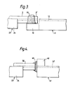
- the potential area of contact between the end face of the optical fibre 32 and the end face of the substrate of the integrated optic device or chip 41 is increased by mounting on the uppermost surface of the substrate a supporting body 48 which overlies the substrate and which has a side face that is substantially co-planar with the side face of the substrate in which the end faces of the optical waveguides 42,43,44... are exposed.
- transparent curable adhesive 49 is introduced between the end face of the optical fibre and the end faces of the substrate and overlying supporting block 48.
- the apparatus illustrated in Figures 1 and 2 can be used to effect permanent connections between the optical fibres 32,33,34... of an optical fibre ribbon and the optical waveguides 42,43,44... of an integrated optic device or chip 41 using the technique illustrated in Figure 4 but, in this case, in effecting accurate axial alignment of the core of each optical fibre in turn and the corresponding optical waveguide, the integrated optic device or chip 41 is so clamped by the clamp 30 that it is fixed and the clamping device 23 is moved with respect to the integrated optic device or chip until the axes of the core of the optical fibre and the corresponding optical waveguide are in axial alignment.
- the improved method of the present invention has the very important advantage that it provides for sequential permanent connection of the optical fibres of a length of optical fibre ribbon with the optical waveguides of an integrated optic device or chip in such a way that each optical fibre of the ribbon is free to move lengthwise to a limited extent with respect to the other optical fibres of the ribbon and that, during permanent connection of any optical fibre with an optical waveguide, the risk that any other optical fibre of the ribbon will be prematurely partially permanently connected to the integrated optic device or chip during such permanent connection of said optical fibre and optical waveguide is substantially reduced.
Landscapes
- Physics & Mathematics (AREA)
- General Physics & Mathematics (AREA)
- Optics & Photonics (AREA)
- Optical Couplings Of Light Guides (AREA)
- Mechanical Coupling Of Light Guides (AREA)
- Light Guides In General And Applications Therefor (AREA)
- Laser Surgery Devices (AREA)
- Optical Integrated Circuits (AREA)
Priority Applications (1)
| Application Number | Priority Date | Filing Date | Title |
|---|---|---|---|
| AT87309916T ATE76202T1 (de) | 1986-11-10 | 1987-11-10 | Kupplung zwischen optischen fasern und optischen wellenleitern. |
Applications Claiming Priority (2)
| Application Number | Priority Date | Filing Date | Title |
|---|---|---|---|
| GB8626816 | 1986-11-10 | ||
| GB868626816A GB8626816D0 (en) | 1986-11-10 | 1986-11-10 | Jointing optical fibres & waveguides |
Publications (3)
| Publication Number | Publication Date |
|---|---|
| EP0274199A2 true EP0274199A2 (fr) | 1988-07-13 |
| EP0274199A3 EP0274199A3 (en) | 1988-07-27 |
| EP0274199B1 EP0274199B1 (fr) | 1992-05-13 |
Family
ID=10607078
Family Applications (1)
| Application Number | Title | Priority Date | Filing Date |
|---|---|---|---|
| EP87309916A Expired - Lifetime EP0274199B1 (fr) | 1986-11-10 | 1987-11-10 | Couplage entre fibres optiques et guides d'ondes optiques |
Country Status (6)
| Country | Link |
|---|---|
| EP (1) | EP0274199B1 (fr) |
| AT (1) | ATE76202T1 (fr) |
| DE (1) | DE3779087D1 (fr) |
| ES (1) | ES2031519T3 (fr) |
| GB (2) | GB8626816D0 (fr) |
| GR (1) | GR3004709T3 (fr) |
Cited By (1)
| Publication number | Priority date | Publication date | Assignee | Title |
|---|---|---|---|---|
| US20110110622A1 (en) * | 2009-11-10 | 2011-05-12 | Furukawa Electric Co., Ltd. | Hybrid integrated optical module |
Families Citing this family (1)
| Publication number | Priority date | Publication date | Assignee | Title |
|---|---|---|---|---|
| EP2542929A1 (fr) | 2010-03-02 | 2013-01-09 | BAE Systems PLC | Fibre optique fixée sur des substrats |
Family Cites Families (1)
| Publication number | Priority date | Publication date | Assignee | Title |
|---|---|---|---|---|
| GB8417911D0 (en) * | 1984-07-13 | 1984-08-15 | British Telecomm | Connecting waveguides |
-
1986
- 1986-11-10 GB GB868626816A patent/GB8626816D0/en active Pending
-
1987
- 1987-11-10 AT AT87309916T patent/ATE76202T1/de not_active IP Right Cessation
- 1987-11-10 DE DE8787309916T patent/DE3779087D1/de not_active Expired - Lifetime
- 1987-11-10 GB GB8726300A patent/GB2197727B/en not_active Expired - Lifetime
- 1987-11-10 EP EP87309916A patent/EP0274199B1/fr not_active Expired - Lifetime
- 1987-11-10 ES ES198787309916T patent/ES2031519T3/es not_active Expired - Lifetime
-
1992
- 1992-05-26 GR GR920401045T patent/GR3004709T3/el unknown
Cited By (2)
| Publication number | Priority date | Publication date | Assignee | Title |
|---|---|---|---|---|
| US20110110622A1 (en) * | 2009-11-10 | 2011-05-12 | Furukawa Electric Co., Ltd. | Hybrid integrated optical module |
| US8503843B2 (en) * | 2009-11-10 | 2013-08-06 | Furukawa Electric Co., Ltd. | Hybrid integrated optical module |
Also Published As
| Publication number | Publication date |
|---|---|
| GB2197727B (en) | 1990-01-10 |
| GB8726300D0 (en) | 1987-12-16 |
| ATE76202T1 (de) | 1992-05-15 |
| GR3004709T3 (fr) | 1993-04-28 |
| EP0274199B1 (fr) | 1992-05-13 |
| DE3779087D1 (de) | 1992-06-17 |
| GB8626816D0 (en) | 1986-12-10 |
| EP0274199A3 (en) | 1988-07-27 |
| ES2031519T3 (es) | 1992-12-16 |
| GB2197727A (en) | 1988-05-25 |
Similar Documents
| Publication | Publication Date | Title |
|---|---|---|
| US4950048A (en) | Optical connector ferrule | |
| US4276113A (en) | Winged V-groove fiber optic clamp and splicer | |
| US4017013A (en) | Multiple fiber end preparation | |
| EP0191064B1 (fr) | Connecteurs de fibres optiques et articles s'y rapportant | |
| US4029390A (en) | Optical fiber group splicing technique and apparatus employing unique foldable holder | |
| EP0637390B1 (fr) | Connecteur de fibres optiques s'utilisant sans adhesif | |
| US4980007A (en) | Methods of fabricating an optical fiber ribbon | |
| US5076881A (en) | Apparatus for fabricating an optical fiber ribbon | |
| US4725297A (en) | Splicing optical fiber ribbon method and apparatus | |
| US6280099B1 (en) | Optical fiber wavelength filter and manufacturing method for the same | |
| JPS5942847B2 (ja) | 光ファイバ接続装置 | |
| US4720161A (en) | Optical fiber coupler-distributer, and method of manufacture | |
| GB2118539A (en) | Precision cleaving of optical fibres | |
| US20170052321A1 (en) | Fused expanded beam connector | |
| EP1312955B1 (fr) | Procédé de couplage pour des fibres optiques | |
| US5216741A (en) | Method of positioning and fixing optical fibres in a row of optical fibres and a coupling device provided with such a row of fibres | |
| JPS61258205A (ja) | 光フアイバ屈曲装置 | |
| EP0274199A2 (fr) | Couplage entre fibres optiques et guides d'ondes optiques | |
| KR20010022335A (ko) | 평면 광학장치 커넥터 및 이의 제조방법 | |
| US7192196B2 (en) | Optical fiber connection component, optical fiber connection structure, and optical fiber connection method | |
| CN88101887A (zh) | 光波导管用的多路连结器 | |
| JP2687145B2 (ja) | 光ファイバ接続具の製造方法 | |
| US5550943A (en) | Unitary, double-ended connector for optical fibres | |
| AU619594B2 (en) | Optical fibre plug pin | |
| JP3062237B2 (ja) | 偏波面保存ファイバ整列用保持体及び同ファイバの整列方法 |
Legal Events
| Date | Code | Title | Description |
|---|---|---|---|
| PUAI | Public reference made under article 153(3) epc to a published international application that has entered the european phase |
Free format text: ORIGINAL CODE: 0009012 |
|
| PUAL | Search report despatched |
Free format text: ORIGINAL CODE: 0009013 |
|
| AK | Designated contracting states |
Kind code of ref document: A2 Designated state(s): AT BE CH DE ES FR GB GR IT LI NL SE |
|
| RHK1 | Main classification (correction) |
Ipc: G02B 6/26 |
|
| AK | Designated contracting states |
Kind code of ref document: A3 Designated state(s): AT BE CH DE ES FR GB GR IT LI NL SE |
|
| 17P | Request for examination filed |
Effective date: 19881109 |
|
| 17Q | First examination report despatched |
Effective date: 19910207 |
|
| RBV | Designated contracting states (corrected) |
Designated state(s): AT BE CH DE ES FR GR IT LI NL SE |
|
| ITF | It: translation for a ep patent filed | ||
| GRAA | (expected) grant |
Free format text: ORIGINAL CODE: 0009210 |
|
| AK | Designated contracting states |
Kind code of ref document: B1 Designated state(s): AT BE CH DE ES FR GR IT LI NL SE |
|
| REF | Corresponds to: |
Ref document number: 76202 Country of ref document: AT Date of ref document: 19920515 Kind code of ref document: T |
|
| ET | Fr: translation filed | ||
| REF | Corresponds to: |
Ref document number: 3779087 Country of ref document: DE Date of ref document: 19920617 |
|
| PGFP | Annual fee paid to national office [announced via postgrant information from national office to epo] |
Ref country code: AT Payment date: 19921013 Year of fee payment: 6 |
|
| PGFP | Annual fee paid to national office [announced via postgrant information from national office to epo] |
Ref country code: BE Payment date: 19921026 Year of fee payment: 6 |
|
| PGFP | Annual fee paid to national office [announced via postgrant information from national office to epo] |
Ref country code: GR Payment date: 19921111 Year of fee payment: 6 |
|
| PGFP | Annual fee paid to national office [announced via postgrant information from national office to epo] |
Ref country code: NL Payment date: 19921130 Year of fee payment: 6 |
|
| REG | Reference to a national code |
Ref country code: ES Ref legal event code: FG2A Ref document number: 2031519 Country of ref document: ES Kind code of ref document: T3 |
|
| REG | Reference to a national code |
Ref country code: GR Ref legal event code: FG4A Free format text: 3004709 |
|
| PLBE | No opposition filed within time limit |
Free format text: ORIGINAL CODE: 0009261 |
|
| STAA | Information on the status of an ep patent application or granted ep patent |
Free format text: STATUS: NO OPPOSITION FILED WITHIN TIME LIMIT |
|
| 26N | No opposition filed | ||
| PG25 | Lapsed in a contracting state [announced via postgrant information from national office to epo] |
Ref country code: AT Effective date: 19931110 |
|
| PG25 | Lapsed in a contracting state [announced via postgrant information from national office to epo] |
Ref country code: BE Effective date: 19931130 |
|
| BERE | Be: lapsed |
Owner name: BICC P.L.C. Effective date: 19931130 |
|
| PG25 | Lapsed in a contracting state [announced via postgrant information from national office to epo] |
Ref country code: GR Free format text: THE PATENT HAS BEEN ANNULLED BY A DECISION OF A NATIONAL AUTHORITY Effective date: 19940531 |
|
| PG25 | Lapsed in a contracting state [announced via postgrant information from national office to epo] |
Ref country code: NL Effective date: 19940601 |
|
| NLV4 | Nl: lapsed or anulled due to non-payment of the annual fee | ||
| REG | Reference to a national code |
Ref country code: GR Ref legal event code: MM2A Free format text: 3004709 |
|
| EAL | Se: european patent in force in sweden |
Ref document number: 87309916.2 |
|
| PGFP | Annual fee paid to national office [announced via postgrant information from national office to epo] |
Ref country code: FR Payment date: 20001018 Year of fee payment: 14 |
|
| PGFP | Annual fee paid to national office [announced via postgrant information from national office to epo] |
Ref country code: SE Payment date: 20001019 Year of fee payment: 14 Ref country code: DE Payment date: 20001019 Year of fee payment: 14 |
|
| PGFP | Annual fee paid to national office [announced via postgrant information from national office to epo] |
Ref country code: CH Payment date: 20001020 Year of fee payment: 14 |
|
| PGFP | Annual fee paid to national office [announced via postgrant information from national office to epo] |
Ref country code: ES Payment date: 20001211 Year of fee payment: 14 |
|
| PG25 | Lapsed in a contracting state [announced via postgrant information from national office to epo] |
Ref country code: SE Free format text: LAPSE BECAUSE OF NON-PAYMENT OF DUE FEES Effective date: 20011111 Ref country code: ES Free format text: LAPSE BECAUSE OF NON-PAYMENT OF DUE FEES Effective date: 20011111 |
|
| PG25 | Lapsed in a contracting state [announced via postgrant information from national office to epo] |
Ref country code: LI Free format text: LAPSE BECAUSE OF NON-PAYMENT OF DUE FEES Effective date: 20011130 Ref country code: CH Free format text: LAPSE BECAUSE OF NON-PAYMENT OF DUE FEES Effective date: 20011130 |
|
| EUG | Se: european patent has lapsed |
Ref document number: 87309916.2 |
|
| PG25 | Lapsed in a contracting state [announced via postgrant information from national office to epo] |
Ref country code: DE Free format text: LAPSE BECAUSE OF NON-PAYMENT OF DUE FEES Effective date: 20020702 |
|
| REG | Reference to a national code |
Ref country code: CH Ref legal event code: PL |
|
| PG25 | Lapsed in a contracting state [announced via postgrant information from national office to epo] |
Ref country code: FR Free format text: LAPSE BECAUSE OF NON-PAYMENT OF DUE FEES Effective date: 20020730 |
|
| REG | Reference to a national code |
Ref country code: FR Ref legal event code: ST |
|
| REG | Reference to a national code |
Ref country code: FR Ref legal event code: ST |
|
| REG | Reference to a national code |
Ref country code: ES Ref legal event code: FD2A Effective date: 20021213 |
|
| PG25 | Lapsed in a contracting state [announced via postgrant information from national office to epo] |
Ref country code: IT Free format text: LAPSE BECAUSE OF NON-PAYMENT OF DUE FEES;WARNING: LAPSES OF ITALIAN PATENTS WITH EFFECTIVE DATE BEFORE 2007 MAY HAVE OCCURRED AT ANY TIME BEFORE 2007. THE CORRECT EFFECTIVE DATE MAY BE DIFFERENT FROM THE ONE RECORDED. Effective date: 20051110 |