EP0274647A1 - Procédé et dispositif de transmission d'un signal numérique de faible débit dans un créneau temporel d'un signal multiplexé dans le temps prévu pour un plus haut débit - Google Patents
Procédé et dispositif de transmission d'un signal numérique de faible débit dans un créneau temporel d'un signal multiplexé dans le temps prévu pour un plus haut débit Download PDFInfo
- Publication number
- EP0274647A1 EP0274647A1 EP87117833A EP87117833A EP0274647A1 EP 0274647 A1 EP0274647 A1 EP 0274647A1 EP 87117833 A EP87117833 A EP 87117833A EP 87117833 A EP87117833 A EP 87117833A EP 0274647 A1 EP0274647 A1 EP 0274647A1
- Authority
- EP
- European Patent Office
- Prior art keywords
- input
- output
- clock
- digital signal
- khz
- Prior art date
- Legal status (The legal status is an assumption and is not a legal conclusion. Google has not performed a legal analysis and makes no representation as to the accuracy of the status listed.)
- Granted
Links
- 238000000034 method Methods 0.000 title claims abstract description 26
- 230000005540 biological transmission Effects 0.000 title claims abstract description 14
- 238000006243 chemical reaction Methods 0.000 claims description 6
- 239000003990 capacitor Substances 0.000 claims description 5
- 230000003111 delayed effect Effects 0.000 claims description 5
- 238000005070 sampling Methods 0.000 abstract description 12
- 230000001360 synchronised effect Effects 0.000 description 3
- 230000001934 delay Effects 0.000 description 2
- 230000015572 biosynthetic process Effects 0.000 description 1
- 238000012217 deletion Methods 0.000 description 1
- 230000037430 deletion Effects 0.000 description 1
- 230000000694 effects Effects 0.000 description 1
- 230000003993 interaction Effects 0.000 description 1
- 239000013589 supplement Substances 0.000 description 1
- 230000007704 transition Effects 0.000 description 1
Images


Classifications
-
- H—ELECTRICITY
- H04—ELECTRIC COMMUNICATION TECHNIQUE
- H04L—TRANSMISSION OF DIGITAL INFORMATION, e.g. TELEGRAPHIC COMMUNICATION
- H04L25/00—Baseband systems
- H04L25/02—Details ; arrangements for supplying electrical power along data transmission lines
- H04L25/05—Electric or magnetic storage of signals before transmitting or retransmitting for changing the transmission rate
-
- H—ELECTRICITY
- H04—ELECTRIC COMMUNICATION TECHNIQUE
- H04J—MULTIPLEX COMMUNICATION
- H04J3/00—Time-division multiplex systems
- H04J3/16—Time-division multiplex systems in which the time allocation to individual channels within a transmission cycle is variable, e.g. to accommodate varying complexity of signals, to vary number of channels transmitted
Definitions
- the invention relates to a method and an arrangement for transmitting a digital signal in a time segment of the pulse frame of a time-division multiplex signal, for which a higher bit rate is made available for transmission in this time segment than the digital signal has.
- a digital signal primary multiplex device is known from the magazine telcom report, 2 (1979) Supplement digital transmission technology, pages 46-51, in which thirty-two synchronous 64 kbit / s signals can be combined to form a 2048 kbit / s time division multiplex signal.
- the object of the invention is to provide a method and an arrangement with which, instead of a 64 kbit / s signal, a digital signal with a bit rate between 0.6 and 19.2 kbit / s can be transmitted losslessly and with as little circuit complexity as possible can. No character distortion should occur with synchronous transmission.
- this object is achieved according to the invention in that the first digital signal is oversampled on the transmission side with a first clock associated with this time segment, that the second digital signal obtained from the oversampling is transmitted in time-division multiplexed signal and that on the receiving side after demultiplexing the second Digital signal is sampled with a second clock corresponding to its bit rate, with the exception of prohibited phase position ranges, if not observed, double sampling would occur.
- the second digital signal is delayed by a period of the first clock and further processed as a third digital signal
- the second digital signal is delayed by two periods of the first clock and is referred to as a fourth digital signal to form a pulse that blocks the forbidden phase position ranges and the second and fourth digital signals are subjected to an antivalence combination.
- FIG. 1 shows a digital signal DS1 with a bit rate of 19.2 kbit / s. This is sampled by a clock T1 with a frequency of 64 kHz, which results in a digital signal DS2 which is transmitted. At the receiving end, this is scanned by a clock T2 with a frequency of 19.2 kHz, the arrows denoting the effective edges. With T2a and T2b there are two Phase positions of the clock T2 designated. Flawless sampling of the digital signal DS2 is possible with the clock T2a. When sampling by the clock T2b, bit errors BF arise from an occasional double sampling.
- FIG. 2 shows the digital signal DS2 and two phase positions T2c and T2d of the clock T2, which include the hatched area of phase positions in which double scans are possible. These areas are referred to as prohibited phase position areas VB.
- FIG. 3 shows a method for obtaining a pulse P, the pulses of which cover the prohibited phase position ranges VB.
- the digital signal DS2 is shifted once to obtain a digital signal DS3 by a period of the clock T1 and on the other hand to generate a digital signal DS4 by two periods of the clock T1.
- the pulse P is derived from the digital signals DS2 and DS4 by an antivalence combination.
- the digital signal DS3 is further processed instead of the digital signal DS2.
- the prohibited phase angle ranges VB are shown below.
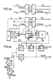
- FIG. 4a shows an arrangement on the transmission side for carrying out the method according to the invention.
- the arrangement contains a shift register 3 for serial-parallel conversion, a shift register 5 for parallel-serial conversion and a line bundle 4 connecting both shift registers 3 and 5.
- a digital signal DS1 with a bit rate of 19.2 kbit / s is applied to input 1, this is implemented in series-parallel with clock T1 at a frequency of 64 kHz at input 2 and fed to shift register 5. There it is read out with the clock T3 of a frequency of 2048 kHz at input 8 when a channel selection signal for one of the thirty-one channels of the 2048 kbit / s time-division multiplex signal in which data transmission is possible is present at input 7.
- the digital signal DS2 is sent out via the output 6.
- FIG. 4b shows an arrangement at the receiving end for carrying out the method according to the invention.
- This arrangement contains shift registers 11, 13 and 17, an exclusive NOR gate 21, an up / down counter 22, a logic 23, D flip-flops 30 and 31, frequency dividers 33, 34, 37 and 38 and a changeover switch 36 .
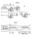
- Figure 5 shows the logic 23 in detail. It contains AND gates 40, 42 and 47, an inverter 41, D flip-flops 43, 44, 45 and 48 and an exclusive OR gate 46.
- a digital signal DS2 received and separated in a demultiplexer is fed to the shift register 11 via the input 9 in FIG. 4b, where it is converted in series-parallel with the clock T3 at the input 10 and entered into the shift register 13 via the connecting line bundle 12. From this it is read out when a channel selection signal is present at input 15 with the clock T1 at input 16 via output 14 and is also entered into the shift register 17 with the clock T1.
- the delays described with reference to FIG. 3 take place there.
- the pulse P appears, which has the effect of a window for the clock T2 in its pulse pauses.
- the clock T2 is generated from the clock T3 at the input 39 of the frequency 2048 kHz by first dividing it in the frequency divider 38 to a frequency of 1536 kHz and then depending on the position of the switch 36 directly or after another division in the frequency divider 37 to a frequency of 307.2 kHz is passed to the inputs of the frequency dividers 33 and 34, which divide in a ratio of 2 n : 1.
- frequencies of 0.75 kHz, 1.5 kHz, 3 kHz, 6 kHz, 12 kHz, 0.6 kHz, 1.2 kHz, 2.4 kHz, 4.8 kHz, 9.6 kHz can be used and generate 19.2 kHz. The latter is selected in the exemplary embodiment.
- bit errors BF can occur during the transmission of the digital signal DS2, it does not make sense to react with an immediate resynchronization of the query time each time the sampling time falls within a prohibited phase position range, especially since this range is also changed by the bit errors BF.
- the up / down counter 22 was therefore provided, which is clocked by the scanning edge. Its counting direction depends on the window around the data edges. If the pulse P is in the logic "L" state (low level), which is possible in the case of double scanning, counting up takes place. If the pulse P is in the logic "H” state (high level), in which no errors are possible, the counting down takes place.
- the up / down counter 22 counts up until a count value "9" is reached. At this value, the max / min output and thus the input 26 change to the logic state "H". Now, on the one hand, the sampling frequency is re-synchronized and, on the other hand, an initial count value is loaded into the up / down counter.
- the pulse P forming the window is located at the input 25 of the inverter 41.
- the inverted signal is thus present at the output of the inverter 41 and thus at an input of the AND gate 40
- Pulse and at the input 26 of this AND gate 40 a pulse both at the count "0" of the up / down counter 22 and at its count "9". Both lie in the event of negative events Inputs at a logic state "H”, then this also occurs at the output of the AND gate 40.
- the output 28 of the AND gate 42 which leads to the clock control (enable) input of the up / down counter 22, then receives a logic state "H” if the logic state at the input 25 is "H" and at entrance 26 is "H". This is the case when errors are impossible due to the pulse P and the count value of the up / down counter 22 has the count value "0". In the event of negative events, however, the output 28 assumes a logic state "L".
- the Q output also receives the logic "H” and the clock T3 Output gives a logic state "L” to output 27 and via this to the set (load) input of the up / down counter 22.
- the logic state "H” at the Q output flips the D flip-flop 44 so that whose Q output also reaches logic "H”.
- the digital signal DS3 present at the input 24 is differentiated in the interaction of the D flip-flop 45 and the exclusive OR gate 46.
- the D flip-flop 45 delays the digital signal DS3 with the clock T3. If there is a logic state "H" at both inputs of the AND gate 47, as occurs when the up / down counter 22 overflows, this state is then converted to the inverted clock synchronized D flip-flop 48 switched through to output 29. There, this state causes a reset of the D flip-flop 44 and the frequency divider 33.
- the frequency divider 33 is erased with any data edge. After the deletion process, the pulse pause of the clock T2 follows and then the transition from the pulse pause to the pulse. This is therefore approximately half a period away from the data edge triggering the process.
- the initial value is loaded to quickly with a new synchronization, which in turn could lead to double scans ler to reach the count "9" so that a new synchronization process is made possible.
- FIG. 6 shows a further arrangement on the receiving side for carrying out the method according to the invention. Compared to that in FIG. 4b, this additionally contains a changeover switch 50, a resistor 51, a switch 52 and a capacitor 54.
- the allowed scanning range is reduced in the window.
- a digital signal further delayed at the output 49 of the shift register 17 than that at the output 20 is applied to the exclusive NOR gate 21 via the changeover switch 50.
- FIG. 7 shows the digital signal DS3, the changed pulse P, the clock T2 with the maximum permissible frequency of 5.3 kHz and the capacitor voltage UC at the measuring point 53.
Landscapes
- Engineering & Computer Science (AREA)
- Computer Networks & Wireless Communication (AREA)
- Signal Processing (AREA)
- Power Engineering (AREA)
- Time-Division Multiplex Systems (AREA)
- Synchronisation In Digital Transmission Systems (AREA)
- Radar Systems Or Details Thereof (AREA)
- Burglar Alarm Systems (AREA)
- Communication Control (AREA)
- Measurement Of Unknown Time Intervals (AREA)
Priority Applications (1)
| Application Number | Priority Date | Filing Date | Title |
|---|---|---|---|
| AT87117833T ATE70929T1 (de) | 1986-12-19 | 1987-12-02 | Verfahren und anordnung zur uebertragung eines digitalsignals niederer bitrate in einem fuer eine hoehere bitrate vorgesehenen zeitabschnitt eines zeitmultiplexsignals. |
Applications Claiming Priority (2)
| Application Number | Priority Date | Filing Date | Title |
|---|---|---|---|
| DE3643561 | 1986-12-19 | ||
| DE3643561 | 1986-12-19 |
Publications (2)
| Publication Number | Publication Date |
|---|---|
| EP0274647A1 true EP0274647A1 (fr) | 1988-07-20 |
| EP0274647B1 EP0274647B1 (fr) | 1991-12-27 |
Family
ID=6316660
Family Applications (1)
| Application Number | Title | Priority Date | Filing Date |
|---|---|---|---|
| EP87117833A Expired - Lifetime EP0274647B1 (fr) | 1986-12-19 | 1987-12-02 | Procédé et dispositif de transmission d'un signal numérique de faible débit dans un créneau temporel d'un signal multiplexé dans le temps prévu pour un plus haut débit |
Country Status (11)
| Country | Link |
|---|---|
| US (1) | US4887261A (fr) |
| EP (1) | EP0274647B1 (fr) |
| JP (1) | JPS63166330A (fr) |
| AT (1) | ATE70929T1 (fr) |
| AU (1) | AU586939B2 (fr) |
| BR (1) | BR8706947A (fr) |
| CA (1) | CA1285339C (fr) |
| DE (1) | DE3775535D1 (fr) |
| ES (1) | ES2028037T3 (fr) |
| GR (1) | GR3003995T3 (fr) |
| NO (1) | NO875275L (fr) |
Cited By (4)
| Publication number | Priority date | Publication date | Assignee | Title |
|---|---|---|---|---|
| EP0731584A3 (fr) * | 1995-03-02 | 1996-11-06 | Bosch Gmbh Robert | Méthode de transmission de données utiles |
| WO2002101938A3 (fr) * | 2001-06-12 | 2003-09-25 | Infineon Technologies Ag | Procede et configuration de circuit pour la transmission de donnees d'un systeme fonctionnant avec une premiere horloge a un systeme fonctionnant avec une deuxieme horloge |
| RU2396721C1 (ru) * | 2009-01-11 | 2010-08-10 | Открытое акционерное общество "Концерн "Созвездие" | Стартстопная система связи |
| RU2396722C1 (ru) * | 2009-04-01 | 2010-08-10 | Открытое акционерное общество "Концерн "Созвездие" | Стартстопная система связи |
Families Citing this family (5)
| Publication number | Priority date | Publication date | Assignee | Title |
|---|---|---|---|---|
| FR2625054B1 (fr) * | 1987-12-18 | 1990-05-04 | Trt Telecom Radio Electr | Dispositif de transformation de paquets de donnees en un multiplex regulier pour systeme de transmission utilisant le principe d'a.m.r.t. |
| US5477364A (en) * | 1989-07-21 | 1995-12-19 | British Telecommunications Public Limited Company | Data transmission on optical networks |
| GB9714215D0 (en) * | 1997-07-04 | 1997-09-10 | Amp Italia | Data transmission method |
| US6845274B2 (en) * | 2001-01-24 | 2005-01-18 | Koninklijke Philips Electronics N.V. | Communication port control module for lighting systems |
| KR101193329B1 (ko) | 2012-01-30 | 2012-10-19 | (주)미래시스템 | 다중채널 실시간 전기적인 신호를 전송하는 방법 |
Citations (4)
| Publication number | Priority date | Publication date | Assignee | Title |
|---|---|---|---|---|
| DE1462579A1 (de) * | 1966-10-11 | 1969-02-06 | Fujitsu Ltd | Schaltung zur Umwandlung von Zeitmultiplexsignalen |
| US3548309A (en) * | 1967-09-14 | 1970-12-15 | Bell Telephone Labor Inc | Data rate converter |
| DE2521731B1 (de) * | 1975-05-15 | 1976-10-07 | Siemens Ag | Verfahren und anordnung zur sendeseitigen asynchronen uebernahme, uebertragung und empfangsseitigen uebergabe digitaler signale |
| US4053708A (en) * | 1976-06-17 | 1977-10-11 | Bell Telephone Laboratories, Incorporated | Asynchronous sample pulse generator |
Family Cites Families (4)
| Publication number | Priority date | Publication date | Assignee | Title |
|---|---|---|---|---|
| FR1486795A (fr) * | 1965-07-16 | 1967-10-05 | ||
| US4230911A (en) * | 1978-08-28 | 1980-10-28 | International Telephone And Telegraph Corporation | Carrier terminal unit |
| JPS5913443A (ja) * | 1982-07-14 | 1984-01-24 | Fuji Xerox Co Ltd | 非同期接続装置 |
| DE3327380A1 (de) * | 1983-07-29 | 1985-02-07 | Siemens AG, 1000 Berlin und 8000 München | Verfahren zur bitraten-tranformation von digitalsignalen |
-
1987
- 1987-11-17 JP JP62288609A patent/JPS63166330A/ja active Granted
- 1987-12-02 AT AT87117833T patent/ATE70929T1/de not_active IP Right Cessation
- 1987-12-02 EP EP87117833A patent/EP0274647B1/fr not_active Expired - Lifetime
- 1987-12-02 DE DE8787117833T patent/DE3775535D1/de not_active Expired - Lifetime
- 1987-12-02 ES ES198787117833T patent/ES2028037T3/es not_active Expired - Lifetime
- 1987-12-03 US US07/128,158 patent/US4887261A/en not_active Expired - Fee Related
- 1987-12-16 NO NO875275A patent/NO875275L/no unknown
- 1987-12-17 CA CA000554582A patent/CA1285339C/fr not_active Expired - Lifetime
- 1987-12-18 AU AU82698/87A patent/AU586939B2/en not_active Ceased
- 1987-12-21 BR BR8706947A patent/BR8706947A/pt not_active IP Right Cessation
-
1992
- 1992-03-11 GR GR910402034T patent/GR3003995T3/el unknown
Patent Citations (4)
| Publication number | Priority date | Publication date | Assignee | Title |
|---|---|---|---|---|
| DE1462579A1 (de) * | 1966-10-11 | 1969-02-06 | Fujitsu Ltd | Schaltung zur Umwandlung von Zeitmultiplexsignalen |
| US3548309A (en) * | 1967-09-14 | 1970-12-15 | Bell Telephone Labor Inc | Data rate converter |
| DE2521731B1 (de) * | 1975-05-15 | 1976-10-07 | Siemens Ag | Verfahren und anordnung zur sendeseitigen asynchronen uebernahme, uebertragung und empfangsseitigen uebergabe digitaler signale |
| US4053708A (en) * | 1976-06-17 | 1977-10-11 | Bell Telephone Laboratories, Incorporated | Asynchronous sample pulse generator |
Non-Patent Citations (1)
| Title |
|---|
| BELL SYSTEM TECHNICAL JOURNAL, Band 61, Nr. 9, Teil 3, November 1982, Seiten 2721-2740, American Telephone and Telegraph Co., Murrax Hill New Jersey, US; T.J. APRILLE et al.: "Dataport - Channel units for digital data system subrates" * |
Cited By (6)
| Publication number | Priority date | Publication date | Assignee | Title |
|---|---|---|---|---|
| EP0731584A3 (fr) * | 1995-03-02 | 1996-11-06 | Bosch Gmbh Robert | Méthode de transmission de données utiles |
| US6009109A (en) * | 1995-03-02 | 1999-12-28 | Robert Bosch Gmbh | Process for transmission of digital application data |
| WO2002101938A3 (fr) * | 2001-06-12 | 2003-09-25 | Infineon Technologies Ag | Procede et configuration de circuit pour la transmission de donnees d'un systeme fonctionnant avec une premiere horloge a un systeme fonctionnant avec une deuxieme horloge |
| US7260734B2 (en) | 2001-06-12 | 2007-08-21 | Infineon Technologies Ag | Method and circuit for transmitting data between systems having different clock speeds |
| RU2396721C1 (ru) * | 2009-01-11 | 2010-08-10 | Открытое акционерное общество "Концерн "Созвездие" | Стартстопная система связи |
| RU2396722C1 (ru) * | 2009-04-01 | 2010-08-10 | Открытое акционерное общество "Концерн "Созвездие" | Стартстопная система связи |
Also Published As
| Publication number | Publication date |
|---|---|
| BR8706947A (pt) | 1988-07-26 |
| US4887261A (en) | 1989-12-12 |
| DE3775535D1 (de) | 1992-02-06 |
| NO875275D0 (no) | 1987-12-16 |
| CA1285339C (fr) | 1991-06-25 |
| NO875275L (no) | 1988-06-20 |
| GR3003995T3 (fr) | 1993-03-16 |
| ES2028037T3 (es) | 1992-07-01 |
| ATE70929T1 (de) | 1992-01-15 |
| JPS63166330A (ja) | 1988-07-09 |
| AU8269887A (en) | 1988-06-23 |
| JPH0371825B2 (fr) | 1991-11-14 |
| AU586939B2 (en) | 1989-07-27 |
| EP0274647B1 (fr) | 1991-12-27 |
Similar Documents
| Publication | Publication Date | Title |
|---|---|---|
| DE69106012T2 (de) | Rahmensynchronisierungsanordnung. | |
| DE2705780C3 (de) | Wiederholungsvorrichtung zum Empfang und Senden von Datensignalen | |
| EP0345564B1 (fr) | Méthode et dispositif de récupération d'une horloge bit d'un signal de télécommunication numérique | |
| EP0036605B1 (fr) | Système MIC avec dispositif de chiffrement du côté de la transmission et dispositif de déchiffrement du côté de la réception | |
| DE69229668T2 (de) | Synchrone Schaltung | |
| DE2838757A1 (de) | Schnittstellenschaltung fuer zeitmultiplexleitungen von nachrichtenvermittlungsanlagen | |
| DE3442613C2 (fr) | ||
| EP0274647B1 (fr) | Procédé et dispositif de transmission d'un signal numérique de faible débit dans un créneau temporel d'un signal multiplexé dans le temps prévu pour un plus haut débit | |
| EP0029607B1 (fr) | Système multiplex à division de temps | |
| EP0363513B1 (fr) | Procedé et dispositif de réception d'un signal numérique binaire | |
| EP0085337B1 (fr) | Système de télécommunications numériques | |
| DE69116494T2 (de) | Rahmensynchronisierungsanordnung | |
| DE2616380B2 (de) | Schaltungsanordnung zur Synchronisierung eines Emgabetaktes mit einem Ausgabetakt bei einem Pufferspeicher für digitale Daten | |
| EP0010662B1 (fr) | Appareil de multiplexage | |
| EP0103163A2 (fr) | Dispositif pour le démultiplexage synchrone d'un signal multiplex à division de temps | |
| EP0419895B1 (fr) | Méthode d'alimentation d'horloge pour les systèmes multiplexes | |
| DE2622107B1 (de) | Verfahren und Anordnung zur digitalen Nachrichtenuebertragung | |
| DE3230027A1 (de) | Synchronisieranordnung | |
| DE2908366C2 (de) | Verfahren und Schaltungsanordnung zur Reduzierung von Phasenschwankungen bei der Taktrückgewinnung in einem digitalen, hierarchisch gegliederten, plesiochronen Nachrichtenübertragungssystem | |
| EP0400398A2 (fr) | Méthode pour recevoir des signaux numériques binaires | |
| DE4041625C2 (fr) | ||
| EP0418641B1 (fr) | Dispositif de synchronisation pour un signal numérique | |
| DE2242639B2 (de) | Zeitmultiplex-telegrafie-system fuer zeichenweise verschachtelung | |
| DE69317242T2 (de) | Rahmen mit mehreren Übertragungsraten und Anordnung zur Multiplexierung von nicht-ganzzahligen Bitraten | |
| DE4434803C1 (de) | Verfahren und Anordnung zur Abtastung eines seriellen Bitstromes |
Legal Events
| Date | Code | Title | Description |
|---|---|---|---|
| PUAI | Public reference made under article 153(3) epc to a published international application that has entered the european phase |
Free format text: ORIGINAL CODE: 0009012 |
|
| AK | Designated contracting states |
Kind code of ref document: A1 Designated state(s): AT BE CH DE ES FR GB GR IT LI NL SE |
|
| 17P | Request for examination filed |
Effective date: 19890109 |
|
| 17Q | First examination report despatched |
Effective date: 19910306 |
|
| GRAA | (expected) grant |
Free format text: ORIGINAL CODE: 0009210 |
|
| AK | Designated contracting states |
Kind code of ref document: B1 Designated state(s): AT BE CH DE ES FR GB GR IT LI NL SE |
|
| REF | Corresponds to: |
Ref document number: 70929 Country of ref document: AT Date of ref document: 19920115 Kind code of ref document: T |
|
| REF | Corresponds to: |
Ref document number: 3775535 Country of ref document: DE Date of ref document: 19920206 |
|
| ET | Fr: translation filed | ||
| ITF | It: translation for a ep patent filed | ||
| GBT | Gb: translation of ep patent filed (gb section 77(6)(a)/1977) | ||
| REG | Reference to a national code |
Ref country code: ES Ref legal event code: FG2A Ref document number: 2028037 Country of ref document: ES Kind code of ref document: T3 |
|
| PLBE | No opposition filed within time limit |
Free format text: ORIGINAL CODE: 0009261 |
|
| STAA | Information on the status of an ep patent application or granted ep patent |
Free format text: STATUS: NO OPPOSITION FILED WITHIN TIME LIMIT |
|
| REG | Reference to a national code |
Ref country code: GR Ref legal event code: FG4A Free format text: 3003995 |
|
| PG25 | Lapsed in a contracting state [announced via postgrant information from national office to epo] |
Ref country code: GB Effective date: 19921202 |
|
| 26N | No opposition filed | ||
| PGFP | Annual fee paid to national office [announced via postgrant information from national office to epo] |
Ref country code: BE Payment date: 19921216 Year of fee payment: 6 |
|
| PGFP | Annual fee paid to national office [announced via postgrant information from national office to epo] |
Ref country code: SE Payment date: 19921218 Year of fee payment: 6 |
|
| PGFP | Annual fee paid to national office [announced via postgrant information from national office to epo] |
Ref country code: FR Payment date: 19921221 Year of fee payment: 6 |
|
| PGFP | Annual fee paid to national office [announced via postgrant information from national office to epo] |
Ref country code: NL Payment date: 19921231 Year of fee payment: 6 |
|
| PGFP | Annual fee paid to national office [announced via postgrant information from national office to epo] |
Ref country code: DE Payment date: 19930218 Year of fee payment: 6 |
|
| PGFP | Annual fee paid to national office [announced via postgrant information from national office to epo] |
Ref country code: CH Payment date: 19930323 Year of fee payment: 6 |
|
| GBPC | Gb: european patent ceased through non-payment of renewal fee |
Effective date: 19921202 |
|
| PGFP | Annual fee paid to national office [announced via postgrant information from national office to epo] |
Ref country code: GR Payment date: 19931119 Year of fee payment: 7 |
|
| PGFP | Annual fee paid to national office [announced via postgrant information from national office to epo] |
Ref country code: AT Payment date: 19931124 Year of fee payment: 7 |
|
| PG25 | Lapsed in a contracting state [announced via postgrant information from national office to epo] |
Ref country code: SE Effective date: 19931203 |
|
| PGFP | Annual fee paid to national office [announced via postgrant information from national office to epo] |
Ref country code: ES Payment date: 19931210 Year of fee payment: 7 |
|
| PG25 | Lapsed in a contracting state [announced via postgrant information from national office to epo] |
Ref country code: LI Effective date: 19931231 Ref country code: CH Effective date: 19931231 Ref country code: BE Effective date: 19931231 |
|
| BERE | Be: lapsed |
Owner name: SIEMENS A.G. Effective date: 19931231 |
|
| PG25 | Lapsed in a contracting state [announced via postgrant information from national office to epo] |
Ref country code: NL Effective date: 19940701 |
|
| NLV4 | Nl: lapsed or anulled due to non-payment of the annual fee | ||
| PG25 | Lapsed in a contracting state [announced via postgrant information from national office to epo] |
Ref country code: FR Effective date: 19940831 |
|
| REG | Reference to a national code |
Ref country code: CH Ref legal event code: PL |
|
| PG25 | Lapsed in a contracting state [announced via postgrant information from national office to epo] |
Ref country code: DE Effective date: 19940901 |
|
| REG | Reference to a national code |
Ref country code: FR Ref legal event code: ST |
|
| PG25 | Lapsed in a contracting state [announced via postgrant information from national office to epo] |
Ref country code: AT Effective date: 19941202 |
|
| PG25 | Lapsed in a contracting state [announced via postgrant information from national office to epo] |
Ref country code: ES Free format text: LAPSE BECAUSE OF EXPIRATION OF PROTECTION Effective date: 19941203 |
|
| EUG | Se: european patent has lapsed |
Ref document number: 87117833.1 Effective date: 19940710 |
|
| PG25 | Lapsed in a contracting state [announced via postgrant information from national office to epo] |
Ref country code: GR Free format text: THE PATENT HAS BEEN ANNULLED BY A DECISION OF A NATIONAL AUTHORITY Effective date: 19950630 |
|
| REG | Reference to a national code |
Ref country code: GR Ref legal event code: MM2A Free format text: 3003995 |
|
| REG | Reference to a national code |
Ref country code: ES Ref legal event code: FD2A Effective date: 20010301 |
|
| PG25 | Lapsed in a contracting state [announced via postgrant information from national office to epo] |
Ref country code: IT Free format text: LAPSE BECAUSE OF NON-PAYMENT OF DUE FEES;WARNING: LAPSES OF ITALIAN PATENTS WITH EFFECTIVE DATE BEFORE 2007 MAY HAVE OCCURRED AT ANY TIME BEFORE 2007. THE CORRECT EFFECTIVE DATE MAY BE DIFFERENT FROM THE ONE RECORDED. Effective date: 20051202 |