EP0274894B1 - Corona-Aufladevorrichtung - Google Patents
Corona-Aufladevorrichtung Download PDFInfo
- Publication number
- EP0274894B1 EP0274894B1 EP19870311271 EP87311271A EP0274894B1 EP 0274894 B1 EP0274894 B1 EP 0274894B1 EP 19870311271 EP19870311271 EP 19870311271 EP 87311271 A EP87311271 A EP 87311271A EP 0274894 B1 EP0274894 B1 EP 0274894B1
- Authority
- EP
- European Patent Office
- Prior art keywords
- corona
- charging device
- generating means
- pins
- wire
- Prior art date
- Legal status (The legal status is an assumption and is not a legal conclusion. Google has not performed a legal analysis and makes no representation as to the accuracy of the status listed.)
- Expired
Links
Images

Classifications
-
- H—ELECTRICITY
- H01—ELECTRIC ELEMENTS
- H01T—SPARK GAPS; OVERVOLTAGE ARRESTERS USING SPARK GAPS; SPARKING PLUGS; CORONA DEVICES; GENERATING IONS TO BE INTRODUCED INTO NON-ENCLOSED GASES
- H01T19/00—Devices providing for corona discharge
- H01T19/04—Devices providing for corona discharge having pointed electrodes
-
- G—PHYSICS
- G03—PHOTOGRAPHY; CINEMATOGRAPHY; ANALOGOUS TECHNIQUES USING WAVES OTHER THAN OPTICAL WAVES; ELECTROGRAPHY; HOLOGRAPHY
- G03G—ELECTROGRAPHY; ELECTROPHOTOGRAPHY; MAGNETOGRAPHY
- G03G15/00—Apparatus for electrographic processes using a charge pattern
- G03G15/02—Apparatus for electrographic processes using a charge pattern for laying down a uniform charge, e.g. for sensitising; Corona discharge devices
- G03G15/0291—Apparatus for electrographic processes using a charge pattern for laying down a uniform charge, e.g. for sensitising; Corona discharge devices corona discharge devices, e.g. wires, pointed electrodes, means for cleaning the corona discharge device
-
- G—PHYSICS
- G03—PHOTOGRAPHY; CINEMATOGRAPHY; ANALOGOUS TECHNIQUES USING WAVES OTHER THAN OPTICAL WAVES; ELECTROGRAPHY; HOLOGRAPHY
- G03G—ELECTROGRAPHY; ELECTROPHOTOGRAPHY; MAGNETOGRAPHY
- G03G2215/00—Apparatus for electrophotographic processes
- G03G2215/02—Arrangements for laying down a uniform charge
- G03G2215/026—Arrangements for laying down a uniform charge by coronas
- G03G2215/028—Arrangements for laying down a uniform charge by coronas using pointed electrodes
Definitions
- the present invention relates to a corona charging device for depositing electrons or negative ions onto an adjacent surface. More particularly, (but not exclusively) it is directed to a corona charging arrangement usable in a xerographic reproduction system for generating a flow of ions onto an adjacent imaging surface for altering or charging the electrostatic charge thereon.
- electrostatic latent image may then be developed and the developed image transferred to a support surface to form a final copy of the original document.
- corona devices are used to perform a variety of other functions in the xerographic process.
- corona devices aid in the transfer of an electrostatic toner image from a reusable photoreceptor to a transfer member, the tacking and detacking of paper to the imaging member, the conditioning of the imaging surface prior to, during, and after the deposition of toner thereon to improve the quality of the xerographic copy produced thereby.
- corona discharge device for use in reproduction systems of the above type is shown generally in US-A-2,836,725 in which a conductive corona electrode in the form of an elongated wire is connected to a corona generating D. C. voltage.
- the wire is partially surrounded by a conductive shield which is usually electrically grounded.
- the surface to be charged is spaced from the wire on the side opposite the shield and is mounted on a grounded substrate.
- a corona device of the above type may be biased in a manner taught in US-A-2,879,395 wherein an A.C. corona generating potential is applied to the conductive wire electrode and a D.C. potential is applied to the conductive shield partially surrounding the electrode to regulate the flow of ions from the electrode to the surface to be charged.
- Other biasing arrangements are known in the prior art and will not be discussed in great detail herein.
- a first problem has been the inability of such devices to deposit relatively uniform negative charge on an imaging surface.
- the charge density varies greatly along the length of the wire resulting in a corresponding variation in the magnitude of charge deposited on associated portions of an adjacent surface to be charged.
- This problem is visually verified as glow spots along the length of the corona wire when negative corona potentials are applied as contrasted to the more uniform corona glow when positive potentials are applied.
- the nonuniformity is believed to result from the fact that negative corona is initiated by high field stripping of electrons from the surface of the wire and sustained in large measure by secondary emission processes at the surface. This secondary emission process is easily affected by surface contamination which typically occurs from chemical growths on these surfaces.
- Positive ion bombardment also is believed to contribute to the nonuniformity problem by partially cleaning portions of the wire, which cleaned portions become emitters of relatively high current with respect to the remainder of the wire.
- US-A-4,086,650 suggests the use of a corona discharge device that includes an A. C. corona discharge electrode located adjacent a conductive shield with the electrode being covered with relatively thick dielectric material so as to substantially prevent the flow of conduction current therethrough.
- the delivery of charge to a photoconductive surface is accomplished by means of displacement current or capacitance coupling through the dielectric material.
- EP-A-0 102-569 shows a large variety of corotrons with wire shaped corona discharge electrodes 3, 4 and 5 in Figure 3 disposed on the surface of a cylinder.
- US-A-4,353,970 discloses a bare wire coronode attached directly to the outside of a glass coated secondary electrode in Figure 5.
- Point coronodes are shown in an electrode arrangement in Figure 10 with their points sticking out away from between two glass plates.
- a corona discharge electrode in contact with or closely spaced from a conductive shield electrode is shown in US-A-4,057,723.
- the discharge electrode includes a conductive wire coated with a relatively thick dielectric material.
- the dielectric is preferably glass, but can be an organic dielectric.
- US-A-4,341,463 discloses two sets of wire coronodes with shields spaced equidistantly around each coronode. The two sets of coronodes are spaced in parallel and not in alternating fashion.
- US-A-4,339,782 a barb coronode with a ring shaped shield spaced equidistantly around the barb tip is shown.
- the shield is perpendicular to the barb and not in the same plane as the barb.
- US-A-4,591,713 discloses a barb coronode with a shield perpendicular to the barb.
- column 6, lines 10 - 12 coronodes of a shieldless corotron are disclosed as taking the form of thin conductive strips which are suitably painted or etched on an appropriate insulating material such as glass or plastic.
- US-A-4,511,244 discloses cleaning a corona wire by generating resistance heating through applying a small EMF directly to the coronode.
- Japanese Patent No. 59-58453 suggests placing a resistor on the back side of a shield which supports a coronode, thereby to heat the air around the coronode and a photosensitive surface being charged in order to try and stabilize the electrified state on the photoreceptor.
- the present invention provides a D.C corona charging device as defined in claim 1.
- An embodiment of the invention comprises a flat scorotron that improves mechanical tolerance, offers low manufacturing costs, greater reliability, requires little maintenance, is easily serviced and includes humidity control means.
- the flat scorotron comprises pin electrodes and reference electrodes coplanar on the surface of the insulating substrate. Self biasing of the configuration is limited, since charging of the insulating substrate will quickly shut off charge flow to it, but will not quench the corona emissions from the pin coronodes.
- An optional heater can be placed on the insulator in order to reduce relative humidity in the region of the coronodes.
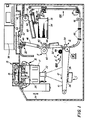
- FIG. 1 schematically depicts the various components of an illustrative electrophotographic copying machine incorporating the improved corona charging device of the present invention therein.
- the illustrative electrophotographic printing machine employs a belt 10 having a photoconductive surface thereon.
- the photoconductive surface is made from a selenium alloy.
- Belt 10 moves in the direction of arrow 12 to advance successive portions of the photoconductive surface through the various processing stations disposed about the path of movement thereof.
- a corona generating device in accordance with the present invention charges the photoconductive surface to a relatively high substantially uniform potential.
- the charged portion of the photoconductive surface is advanced through imaging station B.
- a document handling unit indicated generally by the reference numeral 15, positions original document 16 facedown over exposure system 17.
- the exposure system, indicated generally by reference numeral 17 includes lamp 20 which illuminates document 16 positioned on transparent platen 18.
- the light rays reflected from document 16 are transmitted through lens 22.
- Lens 22 focuses the light image of original document 16 onto the charged portion of the photoconductive surface of belt 10 to selectively dissipate the charge thereof.
- This records an electrostatic latent image on the photoconductive surface which corresponds to the information areas contained within the original document.
- belt 10 advances the electrostatic latent image recorded on the photoconductive surface to development station C.
- Platen 18 is mounted movably and arranged to move in the direction of arrows 24 to adjust the magnification of the original document being reproduced.
- Lens 22 moves in synchronism therewith so as to focus the light image of original document 16 onto the charged portions of the photoconductive surface of belt 10.
- Document handling unit 15 sequentially feeds documents from a stack of documents placed by the operator in a normal forward collated order in a document stacking and holding tray.
- the documents are fed from the holding tray in seriatim, to platen 18.
- the document handling unit recirculates documents back to the stack supported on the tray.
- the document handling unit is adapted to serially sequentially feed the documents, which may be of various sizes and weights of paper or plastic containing information to be copied. The size of the original document disposed in the holding tray and the size of the copy sheet are measured.
- a pair of magnetic brush developer rollers indicated generally by the reference numerals 26 and 28, advance a developer material into contact with the electrostatic latent image.
- the latent image attracts toner particles from the carrier granules of the developer material to form a toner powder image on the photoconductive surface of belt 10.
- belt 10 advances the toner powder image to transfer station D.
- transfer station D a copy sheet is moved into contact with the toner powder image.
- Transfer station D includes a corona generating device 30 which sprays ions onto the backside of the copy sheet. This attracts the toner powder image from the photoconductive surface of belt 10 to the sheet.
- conveyor 32 advances the sheet to fusing station E.
- the copy sheets are fed from tray 34 to transfer station D.
- the tray senses the size of the copy sheets and sends an electrical signal indicative thereof to a microprocessor within controller 38.
- the holding tray of document handling unit 15 includes switches thereon which detect the size of the original document and generate an electrical signal indicative thereof which is transmitted also to a microprocessor controller 38.
- Fusing station E includes a fuser assembly, indicated generally by the reference numeral 40, which permanently affixes the transferred powder image to the copy sheet.
- fuser assembly 40 includes a heated fuser roller 42 and backup roller 44. The sheet passes between fuser roller 42 and backup roller 44 with the powder image contacting fuser roller 42. In this manner, the powder image is permanently affixed to the sheet.
- conveyor 46 transports the sheets to gate 48 which functions as an inverter selector.
- gate 48 the copy sheets will either be deflected into a sheet inverter 50 or bypass sheet inverter 50 and be fed directly onto a second decision gate 52.
- copy sheets which bypass inverter 50 turn a 90° corner in the sheet path before reaching gate 52.
- Gate 48 directs the sheets into a face up orientation so that the imaged side which has been transferred and fused is face up. If inverter path 50 is selected, the opposite is true, i.e., the last printed face is facedown.
- Second decision gate 52 deflects the sheet directly into an output tray 54 or deflects the sheet into a transport path which carries it on without inversion to a third decision gate 56.
- Gate 56 either passes the sheets directly on without inversion into the output path of the copier, or deflects the sheets into a duplex inverter roll transport 58.
- Inverting transport 58 inverts and stacks the sheets to be duplexed in a duplex tray 60 when gate 56 so directs.
- Duplex tray 60 provides intermediate or buffer storage for those sheets which have been printed on one side and on which an image will be subsequently printed on the side opposed thereto, i.e., the copy sheets being duplexed. Due to the sheet inverting by rollers 58, these buffer set sheets are stacked in duplex tray 60 facedown. They are stacked in duplex tray 60 on top of one another in the order in which they are copied.
- the previously simplexed sheets in tray 60 are fed to conveyor 59 seriatim by bottom feeder 62 back to transfer station D for transfer of the toner powder image to the opposed side of the sheet.
- Conveyors 100 and 66 advance the sheet along a path which produces an inversion thereof.
- the proper or clean side of the copy sheet is positioned in contact with belt 10 at transfer station D so that the toner powder image thereon is transferred thereto.
- the duplex sheets are then fed through the same path as the previously simplexed sheets to be stacked in tray 54 for subsequent removal by the printing machine operator.
- Cleaning station F includes a rotatably mounted fibrous brush 68 in contact with the photoconductive surface of belt 10. These particles are cleaned from the photoconductive surface of belt 10 by the rotation of brush 68 in contact therewith.
- a discharge lamp (not shown) floods the photoconductive surface with light to dissipate any residual electrostatic charge remaining thereon prior to the charging thereof for the next successive imaging cycle.
- the wide-spread belief is that as an insulating surface approaches a corona wire, it collects charge, builds up its potential, and supresses the potential gradients around the wire, thereby shutting down corona.
- the fields can be made to prevent ion deposits on the insulating surface, so that its potential does not build up enough to suppress corona substantially.
- a 1.5 mil (0.038 mm) diameter wire can deliver corona currents to a ground plane 1.5mm away, even when the wire is taped to a plexiglas sheet.
- a 10 megohm resistor was connected in between a 2 inch (5.08cm) length of the wire and a power supply.
- corona current to the plate measured about 50 ⁇ A per inch (2.54 cm) in length. With positive voltage, the corona appeared very uniform along the wire. With negative polarity, corona was comparable to that obtained with a wire spanning an open space.
- a charging device of this type carries all conducting elements in one plane, namely, on the surface of a printed circuit board or glass.
- the coronode can be shaped to have "barbs" like sawtooth points to give corona beads at controlled regular intervals.
- the corona points can be made closer together, for example, about 1.5mm or so. This carries significant advantages of ease of manufacture (no stringing and tensioning of fine wires), unlimited length without sagging or singing of wires, durability (no fragile wires to break), and easy maintenance (a single surface can be cleaned with alcohol).
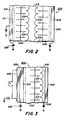
- a flat scorotron 200 is shown that comprises high voltage bus bars 205 and 210 connected to corona lines 212 through overlapping resistor member 230.
- a screen or reference electrode 215 is disclosed for potential leveling purposes and has a low voltage applied to it.
- the whole device is fabricated on a susbstrate 220 such as a printed circuit board or glass using photolithographic techniques.
- a charging device in accordance with the present invention is fabricated by providing a copper clad printed circuit board with a photosensitive overcoating. The printed circuit board is then exposed to a photographic pattern of the conductive elements of the device, such as, the reference electrode, lines or wire(s) and bus bar(s).
- the board is then developed and etched to produce a composite of the conductive elements on the insulating surface.
- Resistive material is then deposited on the board to provide a connection between the bus bar(s) and lines or wire(s).
- the resistive material preferably has a resistance in the range of about 106 to 1010 ohms per square.
- the purpose of connecting each coronode separately to the high voltage D.C. power supply is to prevent arcing, but more importantly to maintain uniform independent corona emission from each coronode with application of sufficiently high potential to the bus bar. For example, the use of a single resistor between the power supply and the bus bar with direct connection of each coronode line to the bus bar results in corona emission from only one coronode tip.
- a high voltage D.C. is preferably applied to the bus bar(s) and a relatively low voltage of approximately (1000 V) applied to the screen or reference electrode. This voltage is adjustable to provide the proper surface potential for charging a receiver.
- a scorotron made by the above described technique in which pin coronodes and a control electrode are positioned coplanar on the surface of an insulator is shown in Figure 2.
- self-biasing of this device is limited, for charging of the insulating substrate will quickly shut off charge flow to it, but will not quench the corona emissions from the pin coronodes.
- high voltage negative, D.C. voltage bus bar(s) 205 and 210 are connected to individual pin electrodes or lines 212 by overlapping current limiting resistive material 230 which preferably has a resistivity range of between about 106 and 1010 ohms.
- a corona is created at the individual pin tips, and is used for charging a photoreceptor surface in scorotron fashion.
- a control electrode 215 has a low voltage applied to it in order to control and predict the potential on the photoreceptor surface.
- Pins 212 extend toward concave, semi-circular portions of electrode and develop a plasma at their tip when biased against a reference.
- the pins are preferably spaced 6 mm on center and 3 mm from the concave, semi-circular portions of the electrode whose boundaries are concentric with each pin.
- the flat scorotron on glass 200 will operate in some high humidity conditions with less efficiency than desired.
- the glass substrate takes in just sufficient moisture to become conducting enough to reduce the potential gradients around the pin ends.
- Improvements have been shown by overcoating the device with very thin hydrophobic films, such as fluorocarbons, silicone resins, etc. However, they do not stand up over long periods of time to the corona chemistry of ionized air.
- a striking effective solution to problems with humidity is to attach a low watt heater, e.g., a resistor, to the back of the device. By heating the device with resistor 211 to about 50° to 60° C, the corona becomes more uniform and stable.
- FIG. 3 An alternative embodiment of the present invention is shown in Figure 3 as flat scorotron 300.
- This scorotron is quite similar to scorotron 200 of Figure 2 except that only one row of pins is shown.
- An insulating substrate 220 has a heating element 330 attached to its back surface and corona pins 212, reference electrode 315, high negative D.C. voltage bus bar 210 etched into its top surface.
- High voltage bus bar 210 is connected to pins 212 by way of resistive material 230 while power supply 308 is directly connected to reference electrode 315.
- Heating element 330 adapts the device for effective and efficient use in a wide range of relative humidities. It is believed that D.C. pins or lines 212 have never been used, before the devices of the present invention, on the surface of an insulator because it was thought that the surface adjacent the pins would charge up, suppressing corona,or requiring higher voltages and producing arcs.
- a novel charging flat scorotron is shown as 80 that comprises an insulator 81 that supports a high voltage bus bar 83 energized by power supply 88 and connected to a corona wire 82 through an overlapping resistor member 85.
- An optional screen or reference electrode 87 is disclosed for potential leveling purposes and has a low voltage applied to it.
- the whole device is fabricated on a thin insulating substrate such as a printed circuit board or glass using photolithographic techniques.
- a charging device in accordance with the present invention is fabricated by providing a copper clad printed circuit board with a photosensitive overcoating.
- the printed circuit board is then exposed to a photographic pattern of the conductive elements of the device, such as, the screen, wire(s) and bus bar.
- the board is then developed and etched to produce a composite of the conductive elements on the insulating surface.
- Resistive material is then deposited on the board to provide a connection between the bus bar and lines or wire(s).
- the resistive material preferably has a resistance in the range of about 106 to 1010 ohms per square. Once the resistive material is on the board, it is ready for use in any of the stations of a machine requiring negative ion production.
- a high voltage D.C. is preferably applied to the bus bar and a relatively low voltage (1000V) applied to the screen. This voltage is adjustable to provide the proper surface potential for charging a receiver.
- a scorotron in which pin coronodes and screen electrodes are coplanar on the surface of an insulator 91 is shown in Figures 5 and 6.
- self-biasing of this device is limited, for charging of the insulating substrate will quickly shut off charge flow to it, but will not quench the corona emissions from the pin coronodes.
- a high voltage negative, D.C. voltage bus bar 95 is connected to individual pin electrodes or lines 93 by current limiting resistive material 94 which preferably has a resistivity range of between about 106 and 1010 ohms.
- a corona is created at the individual pins which is used for charging the surface of a photoreceptor 96 in scorotron fashion.
- a control screen or electrode 92 has a low voltage applied to it in order to control and predict the potential on the photoreceptor surface.
- Pins 93 extend toward concave, semi-circular portions of reference electrode 92 and develop a plasma at their tip when biased against a reference.
- the scorotron device includes a low watt heater attached to a surface thereof to eliminate relative humidity sensitivity and stabilize performance.
- the scorotron device includes a plurality of conductive lines on a top surface of an insulating substrate that are connected to a high voltage negative source of voltage through an overlapping resistive material that enhances corona from the tip, or free end of each line.
- the lines face a charge control electrode that has portions that are concentric with the tip or free end of each line. A small voltage is applied to the control electrode.
- a plurality of lines are shown facing and offset from each other while being separated by a reference electrode in order to control charging streaks.
- a flat scorotron that includes pin coronodes and a reference electrode positioned coplanar on the surface of an insulator with the reference electrode serving to control the amount of charge going to a receiver.
- a line coronode is disposed on a flat, insulating, substrate and connected to a high voltage source through current-limiting resistive material.
- a reference electrode having a low voltage applied to it can be included with this device if desired.
Landscapes
- Physics & Mathematics (AREA)
- Engineering & Computer Science (AREA)
- Plasma & Fusion (AREA)
- General Physics & Mathematics (AREA)
- Electrostatic Charge, Transfer And Separation In Electrography (AREA)
Claims (8)
- Gleichstrom-Corona-Ladevorrichtung zum Übertragen einer gleichförmigen Coronaentladung auf eine Aufnahmeoberfläche mit:
einem isolierenden Substrat (22; 81; 91);
einer Corona-Erzeugungsvorrichtung (212; 82; 93); und
einer Hochspannungserzeugungsvorrichtung (288; 88), die mit der Corona-Erzeugungsvorrichtung verbunden ist;
dadurch gekennzeichnet, daß eine Widerstandsmaterialvorrichtung (230; 85; 94) zwischen der Hochspannungserzeugungsvorrichtung und der Corona-Erzeugungsvorrichtung angeschlossen ist und daß die Corona-Erzeugungsvorrichtung und die Widerstandsmaterialvorrichtung auf einer Oberfläche des Substrats angeordnet sind. - Corona-Ladevorrichtung nach Anspruch 1, die außerdem eine vorgespannte Elektrodenvorrichtung (215; 315; 87; 92) umfaßt, die mit der Corona-Ladevorrichtung koplanar ist und geeignet ist, das durch die Corona-Erzeugungsvorrichtung auf die Aufnahmeoberfläche gebrachte Potential zu regeln.
- Corona-Ladevorrichtung nach Anspruch 1 oder 2, die außerdem eine Heizvorrichtung (211) umfaßt, die auf einer Oberfläche, vorzugsweise einer Bodenfläche, des isolierenden Substrats angeordnet ist und geeignet ist, die Einflüsse der relativen Feuchte auf die Ladevorrichtung zu minimieren.
- Corona-Ladevorrichtung nach einem der vorhergehenden Ansprüche, wobei die Vorrichtung im wesentlichen flach ist.
- Corona-Ladevorrichtung nach einem der vorhergehenden Ansprüche, wobei die Corona-Erzeugungsvorrichtung eine Mehrzahl leitfähiger Stifte umfaßt.
- Corona-Ladevorrichtung nach Anspruch 5, mit wenigsten zwei Reihen dieser Stift.
- Corona-Ladevorrichtung nach Anspruch 6, wobei die wenigstens zwei Stiftreihen einzelne Stifte einer Reihe gestaffelt bezüglich einzelner Stifte einer anderen Reihe besitzen.
- Corona-Ladevorrichtung nach einem der Ansprüche 5 bis 7 zusammen mit Anspruch 2, wobei die Elektrodenvorrichtung konkave, halbkreisförmige Bereiche besitzt, die an Endbereichen der Stifte angrenzend angeordnet sind.
Applications Claiming Priority (2)
| Application Number | Priority Date | Filing Date | Title |
|---|---|---|---|
| US94505586A | 1986-12-22 | 1986-12-22 | |
| US945055 | 1986-12-22 |
Publications (2)
| Publication Number | Publication Date |
|---|---|
| EP0274894A1 EP0274894A1 (de) | 1988-07-20 |
| EP0274894B1 true EP0274894B1 (de) | 1992-06-03 |
Family
ID=25482549
Family Applications (1)
| Application Number | Title | Priority Date | Filing Date |
|---|---|---|---|
| EP19870311271 Expired EP0274894B1 (de) | 1986-12-22 | 1987-12-22 | Corona-Aufladevorrichtung |
Country Status (3)
| Country | Link |
|---|---|
| EP (1) | EP0274894B1 (de) |
| JP (1) | JPS63167383A (de) |
| DE (1) | DE3779604T2 (de) |
Families Citing this family (4)
| Publication number | Priority date | Publication date | Assignee | Title |
|---|---|---|---|---|
| US5361123A (en) * | 1993-08-23 | 1994-11-01 | Xerox Corporation | Microcontroller based xerographic charge device power supply |
| US7187534B2 (en) | 2002-08-29 | 2007-03-06 | Xerox Corporation | Uniform charge device with reduced edge effects |
| US6909867B2 (en) | 2002-08-29 | 2005-06-21 | Xerox Corporation | Uniform charge device with reduced edge effects |
| CN101729963B (zh) * | 2008-10-31 | 2013-03-20 | 宏达国际电子股份有限公司 | 对驻电振膜进行充电的连续式充电设备及其相关方法 |
Family Cites Families (2)
| Publication number | Priority date | Publication date | Assignee | Title |
|---|---|---|---|---|
| DE2064545C3 (de) * | 1970-12-30 | 1980-06-19 | Hoechst Ag, 6000 Frankfurt | Vorrichtung zum elektrostatischen Auf- oder Entladen von Oberflächen eines Materials |
| US4057723A (en) * | 1976-01-23 | 1977-11-08 | Xerox Corporation | Compact corona charging device |
-
1987
- 1987-12-15 JP JP31730987A patent/JPS63167383A/ja active Pending
- 1987-12-22 EP EP19870311271 patent/EP0274894B1/de not_active Expired
- 1987-12-22 DE DE19873779604 patent/DE3779604T2/de not_active Expired - Fee Related
Also Published As
| Publication number | Publication date |
|---|---|
| DE3779604D1 (de) | 1992-07-09 |
| EP0274894A1 (de) | 1988-07-20 |
| JPS63167383A (ja) | 1988-07-11 |
| DE3779604T2 (de) | 1993-02-04 |
Similar Documents
| Publication | Publication Date | Title |
|---|---|---|
| EP0274895B1 (de) | Corona-Aufladevorrichtung | |
| EP0010375B1 (de) | Elektrostatographisches Gerät | |
| US4401383A (en) | Transfer device for use in retention type electrophotographic copying machine | |
| JPS60158582A (ja) | コロナ帯電装置 | |
| US5028779A (en) | Corona charging device | |
| JPS58220160A (ja) | 静電的分離装置およびその方法 | |
| EP0274894A1 (de) | Corona-Aufladevorrichtung | |
| US5043579A (en) | Uniform charging device | |
| US4564282A (en) | Corona charging device | |
| IL31765A (en) | Method and device for the electrostatic charging of surfaces | |
| US4454559A (en) | Control for a corona discharge device | |
| JPH0715608B2 (ja) | 残留トナー除去方法及び装置 | |
| US3122634A (en) | Controlled charging in xerographic copying apparatus | |
| JPH0690568B2 (ja) | 電子写真用帯電装置 | |
| US5666601A (en) | Resistive ion source charging device | |
| US5105223A (en) | Screened blade scorotron | |
| US3640249A (en) | Transfer apparatus | |
| US3954333A (en) | Transfer roll having means for monitoring and controlling the resistivity thereof | |
| JP4017201B2 (ja) | モジュラー充電装置 | |
| EP0816933B1 (de) | Xerographische Vorrichtung und Verfahren zum Aufladen und zur Übertragung | |
| EP0147206A2 (de) | Skorotron mit verteilter Koronawicklung | |
| JP2668951B2 (ja) | 帯電装置用電極素子及びその製造方法 | |
| US5075703A (en) | Ribbon coronode | |
| US4833492A (en) | Charge neutralization for plain paper electrography | |
| US4249064A (en) | Heat fixing device for electrographic apparatus |
Legal Events
| Date | Code | Title | Description |
|---|---|---|---|
| PUAI | Public reference made under article 153(3) epc to a published international application that has entered the european phase |
Free format text: ORIGINAL CODE: 0009012 |
|
| AK | Designated contracting states |
Kind code of ref document: A1 Designated state(s): DE FR GB |
|
| 17P | Request for examination filed |
Effective date: 19890119 |
|
| 17Q | First examination report despatched |
Effective date: 19910213 |
|
| GRAA | (expected) grant |
Free format text: ORIGINAL CODE: 0009210 |
|
| AK | Designated contracting states |
Kind code of ref document: B1 Designated state(s): DE FR GB |
|
| REF | Corresponds to: |
Ref document number: 3779604 Country of ref document: DE Date of ref document: 19920709 |
|
| ET | Fr: translation filed | ||
| PLBE | No opposition filed within time limit |
Free format text: ORIGINAL CODE: 0009261 |
|
| STAA | Information on the status of an ep patent application or granted ep patent |
Free format text: STATUS: NO OPPOSITION FILED WITHIN TIME LIMIT |
|
| 26N | No opposition filed | ||
| PGFP | Annual fee paid to national office [announced via postgrant information from national office to epo] |
Ref country code: FR Payment date: 19951212 Year of fee payment: 9 |
|
| PGFP | Annual fee paid to national office [announced via postgrant information from national office to epo] |
Ref country code: GB Payment date: 19951213 Year of fee payment: 9 |
|
| PGFP | Annual fee paid to national office [announced via postgrant information from national office to epo] |
Ref country code: DE Payment date: 19951222 Year of fee payment: 9 |
|
| PG25 | Lapsed in a contracting state [announced via postgrant information from national office to epo] |
Ref country code: GB Effective date: 19961222 |
|
| GBPC | Gb: european patent ceased through non-payment of renewal fee |
Effective date: 19961222 |
|
| PG25 | Lapsed in a contracting state [announced via postgrant information from national office to epo] |
Ref country code: FR Effective date: 19970829 |
|
| PG25 | Lapsed in a contracting state [announced via postgrant information from national office to epo] |
Ref country code: DE Effective date: 19970902 |
|
| REG | Reference to a national code |
Ref country code: FR Ref legal event code: ST |