EP0275143A2 - Dispositif de lecture d'images - Google Patents
Dispositif de lecture d'images Download PDFInfo
- Publication number
- EP0275143A2 EP0275143A2 EP88300054A EP88300054A EP0275143A2 EP 0275143 A2 EP0275143 A2 EP 0275143A2 EP 88300054 A EP88300054 A EP 88300054A EP 88300054 A EP88300054 A EP 88300054A EP 0275143 A2 EP0275143 A2 EP 0275143A2
- Authority
- EP
- European Patent Office
- Prior art keywords
- level
- white
- intervals
- image signal
- levels
- Prior art date
- Legal status (The legal status is an assumption and is not a legal conclusion. Google has not performed a legal analysis and makes no representation as to the accuracy of the status listed.)
- Ceased
Links
Images


Classifications
-
- H—ELECTRICITY
- H04—ELECTRIC COMMUNICATION TECHNIQUE
- H04N—PICTORIAL COMMUNICATION, e.g. TELEVISION
- H04N1/00—Scanning, transmission or reproduction of documents or the like, e.g. facsimile transmission; Details thereof
- H04N1/40—Picture signal circuits
- H04N1/403—Discrimination between the two tones in the picture signal of a two-tone original
-
- H—ELECTRICITY
- H04—ELECTRIC COMMUNICATION TECHNIQUE
- H04N—PICTORIAL COMMUNICATION, e.g. TELEVISION
- H04N1/00—Scanning, transmission or reproduction of documents or the like, e.g. facsimile transmission; Details thereof
- H04N1/40—Picture signal circuits
- H04N1/40056—Circuits for driving or energising particular reading heads or original illumination means
Definitions
- This invention concerns an image reading device used in electronic print boards, facsimile machines or the like, in particular a device capable of detecting that the light source for illuminating the source document is off.
- a conventional image reader of this type is shown in block diagram of Figure 1.
- 1 represents a lamp for lighting the source document P
- 2 represents a shading plate which smoothes the light intensity distribution of the reflected light L from the source document P
- 3 an image formation lens
- 4 a line sensor which includes a line of photoelectric conversion elements and produces an image signal A.
- 5 is an amplifier for amplifying the image signal read by line sensor 4 to produce an amplified image signal B
- 6 is a comparator which compares the amplified image signal B with a slice level D to produce a series of binary pixel signals
- 7 is a counter for counting the binary signals of a value "1”
- 8 is a control circuit
- 9 is memory
- 10 is D/A converter.
- the image signal produced by line sensor 4 is amplified by amplifier 5, becoming the amplified image signal B, and is input into comparator 6.
- Image signal B is then converted to binary signals F through comparison with slice level D produced by D/A converter 10.
- the peak of one line of image signal is determined and a threshold level to be used in the subsequent actual image reading is determined from the peak thus determined. This is done in the following manner.
- actual image reading means the process of reading data from the area of the source document on which image (characters, symbols, pictures etc. to be processed) has been written.
- the "threshold level” means the slice level D used during actual image reading.
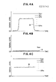
- Figures 2A and 2B are graphs showing relationship between slice levels and the image signals.
- control circuit 8 calls the maximum value of the slice level information (these slice levels are used for finding the peak of the image signal) stored earlier in memory 9; then it inputs into comparator 6 the slice level information E, which is converted at D/A converter 10, receiving the reference voltage Vco, into an analog signal D of a value of slice level VP1.
- line sensor 4 reads one line of an image, and image signal B is input into comparator 6.
- the image signal B is compared with slice level VP1, and is output as binary signals F consisting of "1" and "0" bits.
- Binary signals F of a value "1" are counted by counter 7; the result of counting, G, is then input into control circuit 8.
- control circuit 8 calls from memory 9 slice level information, e.g., VP2, which is one step lower than the previously called slice level information, e.g., VP1. In this way, the control circuit repeats the same operation, gradually decreasing the slice level information until the count value G becomes equal to or greater than the defined value.
- slice level VPj is the largest slice value which gives the count value G of not less than the defined value. Then the slice level VPj is recognized as the peak level and control circuit 8 raises a carry flag, calls from memory 9 the threshold level SLj information corresponding to peak level VPj, sets SLj as threshold level D, then performs actual image reading.
- FIG. 3 Another example of a conventional system uses the configuration shown in block diagram of Figure 3.
- the system in this example differs from that Figure 1 in that it has peak-hold circuit 11 for holding the peak value produced by amplifier 5, and that it varies reference voltage V VAR to be input into D/A converter 10 according to output from peak-hold circuit 11.
- V VAR reference voltage
- This enables the system to lower the threshold level when the light emission intensity from lamp 1 diminishes due to the aging changes or ambient temperature changes.
- This enables the system to set threshold level D consistent with the level of image signal B to enhance the fidelity with which source document P is read.
- the above conventional systems have the following problems.
- the conventional system of Figure 1 is capable of detecting the condition of lamp 1 not lit. However, if the light emission intensity of lamp 1 changes due to the aging or a decrease in the ambient temperature, since threshold level D remains at a fixed level, threshold level D will become inappropriate, resulting in decreased fidelity of image reading relative to the source document image.
- An object of this invention is to provide an image reading device capable of high-fidelity reading of source document images as well as capable of detecting the condition of light source not lit.
- An image reading device comprises a light source for illuminating a medium to be read, a line sensor including a line of photoelectric conversion elements, receiving light from the medium and producing an image signal, means for determining white levels for respective intervals into which said line of photoelectric conversion element are divided, means setting threshold levels for the respective intervals on the basis of said white levels for the respective intervals, means comparing the image signal with said threshold levels to produce a series of binary signals, and means for detecting the condition of light source not lit on the basis of relative magnitude between the white levels for the intervals.
- such detection is made on the basis of the diference between the maximum and minimum of the white levels for the intervals.
- the detection is made on the basis of the white levels for the intervals that adjacent each other and located in a predefined region.
- This embodiment is an image reader used in an electronic print board.
- the electronic print board of this embodiment uses a fluorecent lamp 1 as shown in Fig. 1 to illuminate a source document (medium to be read) which in this embodiment is a movable screen P on which characters, symbols and pictures are written and light reflected from the movable screen P is focused by an image forming lens 3 on a line image sensor such as a linear CCD (charge-coupled device) 4 having a line of multiple, e.g., 1280 photoelectric conversion elements by which the optical input is converted into an electric signal called video or image signal.
- the image signal is compared with a slice level to produce a series of binary pixel signals.
- the binary pixel signals indicate black or white of respective pixels during actual image reading.
- the line sensor comprises 1280 photoelectric conversion elements. This means that the entire height (dimension in the direction parallel to the line) of the screen P consists in effect of 1280 pixels.
- the entire line is evenly divided into n, e.g., 10 sections or intervals and each section consists of 128 pixels.
- the highest of pixel signals (samples of image signal corresponding to respective pixels) within each interval is regarded as the white level for the interval and a threshold level for the interval is determined based on this white level.
- the term “highest” means "m-th highest” where m is a natural number.
- the white level is represented as a digital value of 7 bits, i.e., of 128 steps.
- a line sensor 4 receives reflected light from a screen (recording medium) P on which letters, symbols and/or or pictures are written, and converts the light into electric signal to produce an image signal A by scanning.
- An amplifier 5 amplifies the image signal A to produce an amplified image signal B, which is input to a peak-hold circuit 11 and a comparator 6.
- Peak-hold circuit 11 holds the peak value of the input that has been applied to it, and its output C is input to a reference voltage terminal Vref of a D/A (digital-to-analog) converter 10 to be used as the reference voltage. Supplied to the input data terminal of D/A converter 10 is digital data E from a circuit 8.
- Control circuit 8 has memory 8a which, similar to memory 9 shown in Figure 1, stores a table providing correspondence between white levels and threshold levels. Then, control circuit 8 calls from the correspondence table the threshold level information corresponding to the white level, transferring threshold level E to D/A converter 10.
- D/A converter 10 converts the digital slice level information E into analog slice level signal D using the output (peak value) from the peak-hold circuit 11 as the reference voltage Vref.
- the output D of D/A converter 10 is supplied to the comparator 6 as a threshold level D to be used during the process of actual image reading.
- the output D from the D/A converter is also used as a slice level during the process of determining the white level.
- comparator 6 compares the image signal B with the slice leve D to convert the image signal into a series of binary (pixel) signals F of "1" or "0” depending on whether or not the image signal B is larger than the slice level D.
- the binary signals F are input to arithmetic circuit 12 having functions of multiple (e.g., 10) counters, which are sequentially enabled by the controller 8.
- the counters are alloted to the respective intervals or sections, and each counter is enabled when the pixel signals of the corresponding interval are processed.
- the control circuit 8 in cooperation with each counter serves to determine white level for each interval as defined by the tenth highest value of the pixel signals within the corresponding interval. This is done by the binary search method. More particulary, the slice level for each interval is initially set at the middle, i.e., 128/2.
- Each counter counts the number of "1" pixels in each interval by being enabled while the binary signals of that interval are produced.
- the optimum slice level is thus determined while 6 lines are scanned. This slice level remaining in the counter at the end of the binary search is detected and stored in the control circuit 8, and gives the tenth highest value of the pixel signals and is used as the white level. The reason that the first highest value of the pixel signals is not used as the white level is that there can be a noise which gives rise to especially bright spot which should be ignored.
- the control circuit 8 multiplies the white level with a coefficient, typically having a value between 0.65 and 0.75, e.g. 0.7, to produce a threshold level that should be used during processing of effective data, i.e., data from the area of which the image is to be read and processed.
- a coefficient typically having a value between 0.65 and 0.75, e.g. 0.7
- This multiplication is implemented by use of the memory 8a in the form of a table.
- control circuit 8 sequentially selects the threshold level corresponding to the interval of which the pixel signals are being processed.
- signal "1" at the output of the comparator 6 signifies white (or bright) and "0" signifies black (or dark).
- the peak-hold circuit 11, the D/A converter 10, the arithmetic circuit 12 and the control circuit 8 in combination form a threshold level definition circuit 20 which sets the threshold levels to be input into comparator 6 for actual image reading.
- the image reader of this embodiment is further provided with a maximum value detection circuit 13 which detects the maximum of the white levels of all the intervals and a minimum value detection circuit 14 which detects the minimum of the white levels of all the intervals.
- the maximum value detection circuit 13 and the minimum value detection circuit 14 in combination with the control circuit 8 form a light source "off" detector circuit 30 for lamp 1.
- lamp "off" detector circuit 30 determines that lamp 1 is not lit by the following process.
- the white level information are supplied to maximum value detection circuit 13 and minimum value detection circuit 14.
- control circuit 8 determines that lamp 1 is not lit if the difference between the maximum of the white levels detected by maximum value detection circuit 13 and the minimum of the white levels detected by the minimum value detection circuit 14 is less than the specified value.
- a slice level S is set for the purpose of determining white levels for intervals 1 - n into which the photoelectric convention elements of line sensor 4 are divided. This slice level is identical for all the intervals and is at the middle of the full range (e.g., 128/2).
- Step 2 reads one line of image, and outputs binary signals F by determining whether a given image signal is "1" or "0", based on slice level D set at the above value. Then, arithmetic circuit 12 counts for the intervals 1 - n the number of value "1" bits present.
- step 10 determination is made whether the maximum value Dmax and the minimum value Dmin of the defined white levels set for intervals 1 - n are at least equal to DEF.
- the output value Dmax from maximum value detection circuit 13 occurs near the center where the light intensity is high, and the output value Dmin from minimum value detection circuit 14 occurs toward the edges where the light intensity is low.
- step 10 If the determination at step 10 is positive, then control is transferred to step 11, where a level amounting to 65 to 75% of white levels VP are called from memory 8a and set as threshold levels D, after which actual image reading is performed.
- image signal B, white level VP, and reference voltage Vref converge in the vicinity of OV, as shown in Figure 6B.
- Figure 6C which is an enlargement of Figure 6b along the length of signal level
- the difference Dmax - Dmin becomes very small. Consequently, the condition Dmax - Dmin ⁇ DEF results, and the determination by step 10 becomes negative.
- control is transferred to step 12, where the reading process is cancelled, and the fact that the light source is not lit is indicated by means of an indicator lamp, not shown, or other means.
- this embodiment has a configuration where each line of the image read is split into n intervals, for each interval the white level of an image signal is detected, threshold level D is set according to the detected white level, and at the same time the difference between the maximum and minimum values of the detected white levels is determined, to find whether the light source is lit or not lit. Consequently, as long as light enters even only one interval of the line sensor, the system can determine that the light source is lit.
- the system has a circuit configuration where output signals from the peak-hold circuit are input into the D/A converter as reference voltage, so that even if there is variation in the light intensity from the light source due to the aging changes or change in ambient temperature, images of the source document can be read with good fidelity.
- the device splits each line into n intervals, sets a white level for each interval, and determines whether or not the light source is lit on the basis of the difference between the maximum and minimum values of the white levels detected in the n intervals for a line, the device can determine that the light source is lit, as long as light enters the reading means even in a single interval.
- the device does not mistake the condition of "not lit” for "lit”, and is capable of accurately determining the condition of "not lit”.
- the output signals from the peak-hold circuit are input into the D/A converter as reference electric potential, even if there is variation in the light intensity from the light source due to the aging changes or a change in ambient temperature, high-fidelity reading of images from the source document is possible.
- Fig. 8 shows another embodiment of the invention.
- a control circuit 18 is provided in place of the control circuit 8 of Fig. 5.
- the control circuit 18 has the same functions as the control circuit 8 with regard to determination of the white levels for respective intervals and providing the threshold levels during actual image reading.
- the control circuit 18 differs from the control circuit 8 in the manner of light source "off” detection. Specifically, the control circuit 18 performs the light source "off” detection on the basis of relative magnitudes between white levels for the intervals which are adjacent to each other and located in a predefined region. For instance, where the pattern of the levels of an image signal is generally high at the center and is decreased toward the edges, the control circuit applies all or predetermined ones of the following conditions:
- intervals 2 through J lie on the left of the central interval of maximum light intensity
- intervals K through n-1 lie on the right of it
- intervals 1 and n are intervals with no light input.
- predefined value in conditions (3) and (4) are so set as to be exceeded if any significant amount of light is input in that interval.
- Control circuit 18 determines that the light source is "lit” if the applied conditions are all true, and "not” lit” if any of the conditions is false.
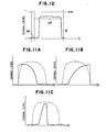
- Figure 9A shows white levels VP obtained by the above series of operations when the light source is lit; image signal B; and reference voltage Vref of D/A converter 16, output from peak-hold circuit 11.
- Intervals 2 through n-1 receive light when the light source remains lit; intervals 1 and n receive no light.
- the white level detected for the intervals 1 and n are about the same as the dark output level of image signal B.
- control circuit 18 Based on the white level of image signal B determined for each interval, control circuit 18 sets threshold level D which is analogous to white level VP of image signal by reference to a correspondence table similar to that in memory 8a in Fig.5, and starts actual reading.
- the output signals from image signal B obtained with the light source lit, reflect characteristics of the light source and lens, forming a pattern in which light intensity is high at the center and decreases toward the edges.
- An example of this effects is illustrated as an image signal B in Figure 9A.
- white levels VP representing the m-th highest pixel signals in respective intervals, show a pattern which is high at the center and decreasing toward the right and the left.
- Figure 9A shows an example of white levels VP.
- the white levels VP of image signal B obtained with the light source not lit represent dark output levels having a very low voltage, forming a generally flat pattern with effects of noise.
- this circuit When flat image signal B is input into peak-hold circuit 11, this circuit outputs a voltage approximately equal to the white levels VP of image signal B; this output, then, is input as reference voltage Vref of D/A converter 10.
- Control circuit 18 searches for white levels VP of image signal B between reference voltage Vref and zero volts, and sets threshold levels D.
- Figure 9B shows reference voltage Vref, image signal B, and white levels VP reflecting the condition of the light source which is not lit.
- Figure 9C is an enlargement of the voltage between reference voltage Vref and zero volts.
- image signal B is shown as a straight line, in actuality it fluctuates up and down due to noise and other effects.
- Peak-hold circuit 11 holds the maximum of image signal B as it fluctuates up and down.
- the follow-up-type binarization circuit detects white levels VP of image signal B for respective intervals. As shown in Figure 9C, white levels thus detected undergo random variations from one interval to another due to effects of random noise.
- the detected white levels of the intervals not receiving light is the dark output level shown for intervals 1 and n in Figure 9A.
- Such dark output levels are considerably lower than reference voltage Vref output from the peak-hold circuit, i.e., the detectable maximum level.
- reference voltage Vref output from the peak-hold circuit with the light source off is about the same as image signal B which has become a dark output level, so that the level for intervals 1 and n may not be detected as a low level.
- reference voltage Vref of D/A converter 10 depends on the peak level of image signal B, even if the absolute level of image signal B is the same, if Vref is high, the absolute level is treated as a low level; if Vref is low, it is treated as a high level. Thus, image signal B is always detected on a relative basis.
- control circuit 18 For each image signal B obtained after the start of reading but before the start of actual data reading, control circuit 18 detects a white level for each interval. It reduces the white levels with a certain ratio from the detected white levels to determine threshold levels D analogous to white levels VP. When it finishes detecting the white levels of image signal B for respective intervals, control circuit 18 uses the following conditions:
- intervals 2 through J lie to the left of the central interval of maximum light intensity
- intervals K through n-1 lie to the right of it
- intervals 1 and n are intervals receiving no light input.
- the predefined value in the condition (3) and (4) are chosen to be exceeded when any significant amount of light enters these intervals.
- Control circuit 18 applies either all of the above conditions or previously specified ones of the above conditions to the white levels detected for the intervals; it determines that the light source is "lit” if the applied conditions are all true, and "not lit” if any of the conditions is false.
- an interval can be set up for the region of no light. Then, given a detected white level, a condition similar to condition (3) or (4), "with a detected white level less than or equal to a specified level” can applied to obtain similar results. If the "specified level” with which the detected white level is compared is varied in proportion to the reference level Vref, i,e., the peak level over the entire line, such judgement on the basis of the conditions (3) and (4) is considered a form of judgement on the basis of relative magnitude of the white levels between intervals.
- the reference voltage Vref of the D/A converter shown in Figure 8 may be held constant. Yet, it can be detected the light source is not lit, by applying the conditions (1) and (2) above.
- the invention is featured in that the condition of the light source not lit is detected on the basis of white levels of the image signal for the respective intervals.
- the white levels are utilized directly for this purpose, i.e., without intervening processing.
- the invention is not limited to such a situation but should be construed to cover such a situation where the white levels are converted into corresponding values, which are then utilized for the detection of light source "off" condition.
- the threshold levels for the respective intervals which are determined on the basis of the respective white levels may be used for the detection of light source "off" condition.
- the embodiment described eliminates the need for incorporating into the device photosensors and other dedicated components for detecting the light source "off” condition, and makes it possible to detect the light source "off” condition through the use of a binarization circuit.
- the device is capable of detecting the light source "off" condition unaffected by changes in light intensity from the light source due to the aging changes or temperature variation.
Landscapes
- Engineering & Computer Science (AREA)
- Multimedia (AREA)
- Signal Processing (AREA)
- Image Input (AREA)
- Facsimile Image Signal Circuits (AREA)
- Facsimile Scanning Arrangements (AREA)
Applications Claiming Priority (4)
| Application Number | Priority Date | Filing Date | Title |
|---|---|---|---|
| JP3337/87 | 1987-01-12 | ||
| JP62003337A JPS63172565A (ja) | 1987-01-12 | 1987-01-12 | 光源不点灯検出装置 |
| JP319327/87 | 1987-12-16 | ||
| JP62319327A JPH01160165A (ja) | 1987-12-16 | 1987-12-16 | 画像読取装置 |
Publications (2)
| Publication Number | Publication Date |
|---|---|
| EP0275143A2 true EP0275143A2 (fr) | 1988-07-20 |
| EP0275143A3 EP0275143A3 (fr) | 1990-10-17 |
Family
ID=26336896
Family Applications (1)
| Application Number | Title | Priority Date | Filing Date |
|---|---|---|---|
| EP19880300054 Ceased EP0275143A3 (fr) | 1987-01-12 | 1988-01-06 | Dispositif de lecture d'images |
Country Status (3)
| Country | Link |
|---|---|
| US (1) | US4876605A (fr) |
| EP (1) | EP0275143A3 (fr) |
| CA (1) | CA1285063C (fr) |
Cited By (3)
| Publication number | Priority date | Publication date | Assignee | Title |
|---|---|---|---|---|
| US4876605A (en) * | 1987-01-12 | 1989-10-24 | Oki Electric Industry Co., Ltd. | Image reading device |
| GB2289183A (en) * | 1994-04-07 | 1995-11-08 | Fujitsu Ltd | White level information correction apparatus |
| EP0539022B1 (fr) * | 1991-09-20 | 1998-04-15 | Toa Medical Electronics Co., Ltd. | Analyseur de particules |
Families Citing this family (10)
| Publication number | Priority date | Publication date | Assignee | Title |
|---|---|---|---|---|
| JPH0286266A (ja) * | 1988-09-21 | 1990-03-27 | Fuji Xerox Co Ltd | 画像読取装置 |
| JPH0732447B2 (ja) * | 1989-05-16 | 1995-04-10 | シャープ株式会社 | 読取装置 |
| JP2776923B2 (ja) * | 1989-11-27 | 1998-07-16 | 株式会社リコー | 原稿読取装置 |
| US5170267A (en) * | 1990-09-28 | 1992-12-08 | Xerox Corporation | Raster input scanner (RIS) with diagnostic mode to predict and verify illumination optical performance |
| US5377282A (en) * | 1991-09-19 | 1994-12-27 | International Business Machines Corporation | Optical inspection system utilizing dynamic analog-to-digital thresholding |
| US5726771A (en) * | 1994-10-31 | 1998-03-10 | Hewlett-Packard Company | System and method for optimizing tonal resolution in an optical scanner |
| US7651474B2 (en) * | 1999-10-01 | 2010-01-26 | Caridianbct, Inc. | Method and apparatus for leukoreduction of red blood cells |
| US20080022872A1 (en) * | 2006-07-28 | 2008-01-31 | The Procter & Gamble Company | Apparatus for perforating printed or embossed substrates |
| JP4345834B2 (ja) * | 2007-03-28 | 2009-10-14 | セイコーエプソン株式会社 | 画像処理装置、印刷装置および画像処理方法 |
| EP2445180B1 (fr) | 2010-10-22 | 2015-06-17 | BlackBerry Limited | Procédé et système pour placer un appel d'urgence vers une entreprise à partir d'un dispositif de communication mobile |
Family Cites Families (14)
| Publication number | Priority date | Publication date | Assignee | Title |
|---|---|---|---|---|
| US4325086A (en) * | 1979-04-20 | 1982-04-13 | Canon Kabushiki Kaisha | Recording device |
| US4516174A (en) * | 1980-03-10 | 1985-05-07 | Ricoh Company, Ltd. | Video signal regulating apparatus |
| JPS5784670A (en) * | 1980-11-17 | 1982-05-27 | Fujitsu Ltd | Video signal read-in system |
| JPS57150277A (en) * | 1981-03-13 | 1982-09-17 | Fuji Xerox Co Ltd | Image signal processing circuit |
| US4481666A (en) * | 1981-12-18 | 1984-11-06 | Kowa Company, Ltd. | Reading-out apparatus |
| JPS58202666A (ja) * | 1982-05-21 | 1983-11-25 | Ricoh Co Ltd | 2値化方式 |
| EP0132841B1 (fr) * | 1983-07-25 | 1987-11-04 | Hitachi, Ltd. | Circuit de traitement de signal pour une caméra de télévision |
| US4709274A (en) * | 1983-08-29 | 1987-11-24 | Canon Kabushiki Kaisha | Image processing apparatus |
| JPS6059867A (ja) * | 1983-09-12 | 1985-04-06 | Canon Inc | 2値化装置 |
| JPS60162377A (ja) * | 1984-02-01 | 1985-08-24 | Sharp Corp | フアクシミリ,ocr等における調光装置 |
| JPS60214154A (ja) * | 1984-04-09 | 1985-10-26 | Sharp Corp | 画像読取装置 |
| JPS6184967A (ja) * | 1984-10-03 | 1986-04-30 | Oki Electric Ind Co Ltd | スライスレベル決定回路 |
| US4763200A (en) * | 1985-04-11 | 1988-08-09 | Minolta Camera Kabushiki Kaisha | Image output apparatus |
| US4876605A (en) * | 1987-01-12 | 1989-10-24 | Oki Electric Industry Co., Ltd. | Image reading device |
-
1987
- 1987-12-31 US US07/140,509 patent/US4876605A/en not_active Expired - Fee Related
-
1988
- 1988-01-06 EP EP19880300054 patent/EP0275143A3/fr not_active Ceased
- 1988-01-08 CA CA000556153A patent/CA1285063C/fr not_active Expired - Fee Related
Cited By (5)
| Publication number | Priority date | Publication date | Assignee | Title |
|---|---|---|---|---|
| US4876605A (en) * | 1987-01-12 | 1989-10-24 | Oki Electric Industry Co., Ltd. | Image reading device |
| EP0539022B1 (fr) * | 1991-09-20 | 1998-04-15 | Toa Medical Electronics Co., Ltd. | Analyseur de particules |
| GB2289183A (en) * | 1994-04-07 | 1995-11-08 | Fujitsu Ltd | White level information correction apparatus |
| GB2289183B (en) * | 1994-04-07 | 1998-03-04 | Fujitsu Ltd | White level information correction apparatus |
| US5732165A (en) * | 1994-04-07 | 1998-03-24 | Fujitsu Limited | White level information correction apparatus for image reading apparatus and image reading apparatus with white level information correction apparatus |
Also Published As
| Publication number | Publication date |
|---|---|
| US4876605A (en) | 1989-10-24 |
| EP0275143A3 (fr) | 1990-10-17 |
| CA1285063C (fr) | 1991-06-18 |
Similar Documents
| Publication | Publication Date | Title |
|---|---|---|
| US4903143A (en) | Image processing apparatus | |
| US5293430A (en) | Automatic image segmentation using local area maximum and minimum image signals | |
| US4554583A (en) | Shading correction device | |
| US4876605A (en) | Image reading device | |
| US5097520A (en) | Method of obtaining optimum threshold values | |
| US5699454A (en) | Image processing apparatus | |
| US4850029A (en) | Adaptive threshold circuit for image processing | |
| JP3334385B2 (ja) | 画像読み取り装置および読み取り方法 | |
| US4853793A (en) | Circuit for converting a video signal produced by a line image sensor into a binary signal on the basis of reference levels determined for sections of the line image sensor using respective counters | |
| US6411735B1 (en) | Method and apparatus for distinguishing between noisy continuous tone document types and other document types to maintain reliable image segmentation | |
| EP0195925A2 (fr) | Procédé pour transformer des niveaux de gris d'images | |
| US4881188A (en) | Binary coding circuit | |
| JP3215146B2 (ja) | 画像処理装置 | |
| US20030011828A1 (en) | High-speed calibration method and system for an image-capture apparatus | |
| EP0569063B1 (fr) | Décalage automatique et contrÔle d'amplification dans un analyseur de documents | |
| JPH03143012A (ja) | 2値化回路、中間レベル検出回路及びピーク包絡線検出回路 | |
| JP3027400B2 (ja) | 画像2値化回路 | |
| JP2552315B2 (ja) | 画像読取装置 | |
| JP2752527B2 (ja) | 中間調処理回路 | |
| JP3130556B2 (ja) | 画像読取装置 | |
| JPS631249A (ja) | 画像読取装置 | |
| JP2740366B2 (ja) | 画像信号のコントラスト強調方法およびこれを用いた画像信号の2値化装置 | |
| JPS6339141B2 (fr) | ||
| JPH0618439B2 (ja) | 画像処理装置 | |
| JPH0575849A (ja) | 画像領域識別装置 |
Legal Events
| Date | Code | Title | Description |
|---|---|---|---|
| PUAI | Public reference made under article 153(3) epc to a published international application that has entered the european phase |
Free format text: ORIGINAL CODE: 0009012 |
|
| AK | Designated contracting states |
Kind code of ref document: A2 Designated state(s): FR GB SE |
|
| PUAL | Search report despatched |
Free format text: ORIGINAL CODE: 0009013 |
|
| AK | Designated contracting states |
Kind code of ref document: A3 Designated state(s): FR GB SE |
|
| 17P | Request for examination filed |
Effective date: 19901215 |
|
| 17Q | First examination report despatched |
Effective date: 19921106 |
|
| STAA | Information on the status of an ep patent application or granted ep patent |
Free format text: STATUS: THE APPLICATION HAS BEEN REFUSED |
|
| 18R | Application refused |
Effective date: 19931018 |