EP0275920A2 - Récepteur optique hétérodyne comportant un coupleur optique et un amplificateur électronique - Google Patents
Récepteur optique hétérodyne comportant un coupleur optique et un amplificateur électronique Download PDFInfo
- Publication number
- EP0275920A2 EP0275920A2 EP88100399A EP88100399A EP0275920A2 EP 0275920 A2 EP0275920 A2 EP 0275920A2 EP 88100399 A EP88100399 A EP 88100399A EP 88100399 A EP88100399 A EP 88100399A EP 0275920 A2 EP0275920 A2 EP 0275920A2
- Authority
- EP
- European Patent Office
- Prior art keywords
- output
- receiver according
- input
- coupler
- receiver
- Prior art date
- Legal status (The legal status is an assumption and is not a legal conclusion. Google has not performed a legal analysis and makes no representation as to the accuracy of the status listed.)
- Granted
Links
Images

Classifications
-
- H—ELECTRICITY
- H04—ELECTRIC COMMUNICATION TECHNIQUE
- H04B—TRANSMISSION
- H04B10/00—Transmission systems employing electromagnetic waves other than radio-waves, e.g. infrared, visible or ultraviolet light, or employing corpuscular radiation, e.g. quantum communication
- H04B10/60—Receivers
- H04B10/61—Coherent receivers
Definitions
- the invention relates to an optical superimposed receiver according to the preamble of patent claim 1.
- a receiver of the type mentioned is known for example from IEE Colloquium on Advances in Coherent Optic Devices and Technologies, Savoy Place, London, GB, March 1985 and from ECOC '86, pp. 395-398.
- an optical ASK multiport homodyne receiver is described, in which the transmit and oscillator signals are brought together via an optical coupler in the form of a 3 ⁇ 3 coupler, with a different relative phase shift of the two incident signals at the outputs of this coupler .
- the relative phase difference between the three mixed signal components which can be taken from the 3 ⁇ 3 coupler must be 120 ° in each case and the coupler is not easy to manufacture.
- the three mixed signal components are fed to three separate amplifiers of the electronic amplifier part.
- 90 ° hybrids for example, homodyne receivers (see Journ. Of Lightwave Technology, LT-3 (1985), pp. 1238-1247 and multiport receivers (see also Electron. Lett. 21 (1985) pp. 867-868)
- Optical hybrids for free beam propagation are known (see also AEÜ 37 (1983) pp. 203-206), in which the 90 ° shift of the two orthogonal field strength components of a circularly polarized light source is exploited.
- Overlay system however, one would like to implement all optical components in waveguide technology.
- a 90 ° hybrid has also become known (see Ed 1 Sti / 22.1.1986 also DW Stowe, Paper TUB 5, OFC-83, (New Orleans)), which is realized with four interconnected fiber directional couplers and a phase shifter.
- the object of the invention is to provide an optical heterodyne receiver with an optical coupler device which can be produced relatively easily using integrated waveguide technology and in which the amplitude noise of the oscillator signal of the local oscillator is largely suppressed.
- the coupler device of the receiver according to the invention is a special 90 ° hybrid, in which the phase shift between the two mixed signal components and the phase shift between the other two mixed signal components is also specifically 180 °.
- the two compensating amplifiers of the electronic amplifier part form a so-called "balanced receiver” (see Journ. Of Lightwave Technology, LT-3 (1985) pp. 1110-1122). Accordingly, the receiver according to the invention can essentially be regarded as a combination of an optical 90 ° hybrid with a "balanced receiver” which is novel.
- an actuator and a control device are provided.
- the 90 ° phase difference between the two mixed signal components and the other two mixed signal components at the output gates of the optical 90 ° hybrid is reliably ensured by the readjustment.
- Appropriate choice of control dynamics and control speed can compensate for thermal and mechanical influences.
- a preferred embodiment of the control device which uses the intermediate frequency between the frequency of the transmission signal and the frequency of the local oscillator signal, is specified in claim 3.
- the actuator is preferably arranged according to claim 4 in the coupler device itself.
- the output signal of one of the two compensating amplifiers can be fed via a bandpass filter to a frequency discriminator, which adjusts the local oscillator in terms of the optical frequency.
- a frequency discriminator which adjusts the local oscillator in terms of the optical frequency.
- this coupler device according to claim 6 is specified in claims 7 to 17.
- the 90 ° phase difference can be set in the coupler device in different ways.
- the coupler device can be formed in a substrate made of electro-optical or magneto-optical material.
- the 90 ° phase difference can be set or changed via electrical or magnetic fields, which provides a new type of adjustable coupler device. This case is particularly suitable for the above-mentioned readjustment of the phase difference. It is expedient if the phase shifter consists of an electro-optical or magneto-optical phase modulator.
- the propagation constant of the light in the underlying waveguide section can be changed slightly so long that the desired phase difference is reached.
- this phase difference could also be achieved by waveguides of different lengths, in which the propagation constant of the light is the same.
- the phase shifter would be realized by the applied or etched-off dielectric cover layer or the difference in length.
- the manufacture of the coupler device using planar technology (claim 13) is particularly recommended because it enables a low-drift and stable optical hybrid to be obtained.
- the waveguides can be produced, for example, by ion exchange in glasses (claim 14) or by the diffusion of titanium in LiNbO3.
- the input and output couplers can be directional couplers (claims 7 and 10). Instead of the directional coupler, x-shaped crossovers (claims 9 and 11) can be used, as they are similar to Journ. of Lightwave Technology, LT-3 (1985) pp. 635-642.
- the directional coupler on the input side can also be y-shaped waveguide branches (claim 12).
- the directional couplers on the input side can have asymmetrical divider ratios.
- the division ratio is expediently 1: 1 (claim 8), i.e. they are expediently designed as a 3 dB coupler.
- the divider ratios of the directional couplers on the input side of the coupler device must be optimized in accordance with the data rate and the phase noise of the lasers used (see Journ. Of Lightwave Technology, LT-3 (1985), pp. 1238-1247).
- the division ratio of the two input-side couplers should be as precisely as possible 1: 1 (claim 17), i.e. they should be designed as a 3 dB coupler.
- phase shifter in the coupler device according to claim 6 can be arranged between any output port of an input-side coupler and the assigned input port of the relevant output-side coupler.
- the heterodyne receiver according to the invention can be, for example, an ASK multiport receiver (see claim 18), a PSK homodyne receiver (see claim 19) or else a DPSK heterodyne receiver (see claim 20).
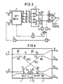
- All of the receivers shown in FIGS. 1 to 3 contain the essential part of the 90 ° hybrid 1 and the electronic amplifier part with the compensating amplifiers 21 and 22, which are designed as differential amplifiers and together form the so-called "balanced receiver".
- the transmission signal E1 is coupled in via the input e1 of the 90 ° hybrid, while the oscillator signal E2 of the local oscillator 3 is input via the other input e2 of the hybrid.
- the transmission signal E1 is a PSK signal.
- the transmission signal is a DPSK or ASK signal.
- the 90 ° hybrid works so that in it the transmission signal E1 and the oscillator signal E2 is mixed in two optical couplers and then four mixed signal components A1 to A4 from the two generated mixed signals are output in parallel at the output gates A1 to A4 of the hybrid, the Mixed signal components A1 and A2 by 180 ° and the mixed signal components A3 and A4 are also 180 ° out of phase with each other.
- the two mixed signal components A1 and A2 are phase-shifted by 90 ° against the two mixed signal components A3 and A4.
- the four mixed signal components A1 to A4 are supplied to assigned optoelectric detectors b1 to b4 and converted there into corresponding electrical signals.
- the electrical signals corresponding to the mixed signal components A1 and A2 are fed to the two inputs of the differential amplifier 21, while the electrical signals corresponding to the mixed signal components A3 and A4 are fed to the differential inputs of the other differential amplifier 22.
- the circuit part connected to the outputs c1 and c2 of the amplifier part 2 with the data output from electron.
- the output signals U21 and U43 of the amplifiers 21 and 22 are rectified by full-wave rectifiers 61 and 62 and then summed up by a summing device 7. The resulting signal contains the complete information of the transmission signal and can then be demodulated.
- This receiver also contains a control device which regulates the phase difference between the two output signals of the two compensating amplifiers 21 and 22 and, in the event of a deviation of the actual value from the setpoint 90 °, via a phase modulator arranged in a 90 ° hybrid, the phase difference back to the setpoint.
- the control signal for the optical phase shifter of the 90 ° hybrid 1 is generated from the two output signals U21 and U43 of the amplifiers 21 and 22. These signals are fed to the multiplier 43 via the bandpass filters 41 and 42 at the center frequency, which corresponds to the intermediate frequency, the output signal of which is integrated via the low-pass filter 44 and fed to the phase shifter.
- This phase shifter extends the 90 ° hybrid to an adjustable hybrid in which the phase difference can be set.
- the output signal from one of the two band-pass filters 41 and 42 is fed to a frequency discriminator 5, which adjusts the local oscillator 3 according to the optical frequency.
- FIG. 4 shows the internal structure of the adjustable hybrid, which is suitable as a 90 ° hybrid for the receivers described above.
- Four optical directional couplers RK1 to RK4 are integrated on the surface of the substrate S made of, for example, LiNbO3 and are guided by the waveguides WL1 to WL4 are connected in a certain way.
- the waveguides of the directional couplers and the connecting waveguides WL1 to WL4 are, for example, Ti-diffused strip waveguides.
- the two left-hand directional couplers RK1, RK2 form the input-side couplers, while the right-hand directional couplers RK3 and RK4 form the two output-side couplers of the hybrid.
- the one output port d1 of the left-hand directional coupler RK1 is only connected to the associated input port d31 of the output-side directional coupler RK3 through the waveguide WL1, while the other output port d2 of the input-side directional coupler RK1 through the waveguide WL2 is only connected to the input port d41 of the other output-side directional coupler is.
- FIG. 4 the type of connection shown in FIG. 4 is only an example. It could also be connected differently, it is important that the four output gates d1 to d4 of the input-side couplers RK1 and RK2 are reversibly and uniquely assigned to the input gates d31, d32, d41 and d42 and that each input-side coupler RK1 and RK2 with the two output sides Couplers RK3 and RK4 is connected.
- the phase of the light guided in the waveguide WL4 can be influenced by the phase modulator PS, by means of which the 90 ° phase difference or also another phase difference can be set.
- the modulator PS is an electro-optical modulator in the present case and consists essentially of two electrodes arranged on both sides of the waveguide WL4 and applied to the substrate S electrodes El 1 and El 2, via which a voltage difference can be applied.
- Such modulators are known from the literature.
- the phase modulator PS can be assigned to the waveguide WL4. It can be arranged such that it does not influence the phase of the light guided in the waveguide 4, but rather the phase of the light guided in any other connecting waveguide.
- control signal can be supplied to one of the two electrodes of the modulator PS, for example the electrode El 1, as the control voltage, while the other electrode El 2 is connected to ground.
- the output gates of the output-side couplers RK3 and RK4 form the four outputs a1 to a4 of the hybrid.
Landscapes
- Physics & Mathematics (AREA)
- Electromagnetism (AREA)
- Engineering & Computer Science (AREA)
- Computer Networks & Wireless Communication (AREA)
- Signal Processing (AREA)
- Optical Communication System (AREA)
- Digital Transmission Methods That Use Modulated Carrier Waves (AREA)
- Optical Integrated Circuits (AREA)
Applications Claiming Priority (2)
| Application Number | Priority Date | Filing Date | Title |
|---|---|---|---|
| DE3701793 | 1987-01-22 | ||
| DE3701793 | 1987-01-22 |
Publications (3)
| Publication Number | Publication Date |
|---|---|
| EP0275920A2 true EP0275920A2 (fr) | 1988-07-27 |
| EP0275920A3 EP0275920A3 (en) | 1990-05-30 |
| EP0275920B1 EP0275920B1 (fr) | 1993-11-03 |
Family
ID=6319309
Family Applications (1)
| Application Number | Title | Priority Date | Filing Date |
|---|---|---|---|
| EP88100399A Expired - Lifetime EP0275920B1 (fr) | 1987-01-22 | 1988-01-13 | Récepteur optique hétérodyne comportant un coupleur optique et un amplificateur électronique |
Country Status (4)
| Country | Link |
|---|---|
| US (1) | US4829598A (fr) |
| EP (1) | EP0275920B1 (fr) |
| JP (1) | JP2519188B2 (fr) |
| DE (1) | DE3885310D1 (fr) |
Cited By (1)
| Publication number | Priority date | Publication date | Assignee | Title |
|---|---|---|---|---|
| EP1986352A3 (fr) * | 2007-04-27 | 2009-04-01 | Fujitsu Limited | Récepteur optique |
Families Citing this family (17)
| Publication number | Priority date | Publication date | Assignee | Title |
|---|---|---|---|---|
| EP0352809B1 (fr) * | 1988-07-29 | 1997-04-16 | Nec Corporation | Récepteur optique hétérodyne à diversité de polarisation avec ajustement de la phase de deux signaux à fréquence intermédiaire pour la commande d'une source optique locale |
| CA1323657C (fr) * | 1989-09-22 | 1993-10-26 | Mohsen Kavenrad | Recepteur homodyne optique mdpd dote d'un amplificateur de lumiere |
| US5060312A (en) * | 1990-03-05 | 1991-10-22 | At&T Bell Laboratories | Polarization independent coherent lightwave detection arrangement |
| US6556326B2 (en) * | 1996-12-20 | 2003-04-29 | Tyco Telecommunications (Us) Inc. | Synchronous amplitude modulation for improved performance of optical transmission systems |
| US20040161245A1 (en) * | 1996-12-20 | 2004-08-19 | Bergano Neal S. | Synchronous amplitude modulation for improved performance of optical transmission systems |
| US6321000B1 (en) * | 1998-12-01 | 2001-11-20 | Nortel Networks Limited | Optical equalizer |
| JPWO2002031965A1 (ja) * | 2000-10-12 | 2004-02-26 | ソニー株式会社 | 復調器およびそれを用いた受信機 |
| US7327913B2 (en) * | 2001-09-26 | 2008-02-05 | Celight, Inc. | Coherent optical detector and coherent communication system and method |
| ITTO20030708A1 (it) * | 2003-09-16 | 2005-03-17 | Istituto Superiore Mario Boella Sul Le Tecnologie | Oscillatore ottico controllato in tensione per un anello |
| US7406269B2 (en) * | 2006-03-10 | 2008-07-29 | Discovery Semiconductors, Inc. | Feedback-controlled coherent optical receiver with electrical compensation/equalization |
| US7809284B2 (en) * | 2006-06-23 | 2010-10-05 | Alcatel-Lucent Usa Inc. | System and method for receiving coherent, polarization-multiplexed optical signals |
| JP2012198292A (ja) * | 2011-03-18 | 2012-10-18 | Fujitsu Ltd | 光ハイブリッド回路及び光受信機 |
| US8849130B2 (en) * | 2011-09-20 | 2014-09-30 | Alcatel Lucent | Coherent optical receivers for colorless reception |
| US9917672B2 (en) | 2013-08-09 | 2018-03-13 | Technical University Of Denmark | Wireless distributed antenna MIMO |
| EP3399671A1 (fr) | 2014-02-07 | 2018-11-07 | Danmarks Tekniske Universitet | Décodage d'une amplitude modulée combinée et signal modulé de fréquence |
| JP6204272B2 (ja) * | 2014-06-05 | 2017-09-27 | 日本電信電話株式会社 | 距離計測装置 |
| JP7380329B2 (ja) * | 2020-02-28 | 2023-11-15 | 富士通オプティカルコンポーネンツ株式会社 | 光回路デバイス、及び光受信機 |
Family Cites Families (4)
| Publication number | Priority date | Publication date | Assignee | Title |
|---|---|---|---|---|
| GB2172766B (en) * | 1985-03-21 | 1988-12-21 | Stc Plc | Optical receiver |
| CA1290019C (fr) * | 1986-06-20 | 1991-10-01 | Hideo Kuwahara | Recepteur de signaux lumineux a dedoublement |
| DE3621734A1 (de) * | 1986-06-28 | 1988-01-07 | Standard Elektrik Lorenz Ag | Optischer ueberlagerungsempfaenger |
| US4718120A (en) * | 1986-11-24 | 1988-01-05 | American Telephone And Telegraph Company, At&T Bell Laboratories | Polarization insensitive coherent lightwave detector |
-
1987
- 1987-12-28 US US07/137,966 patent/US4829598A/en not_active Expired - Fee Related
-
1988
- 1988-01-13 EP EP88100399A patent/EP0275920B1/fr not_active Expired - Lifetime
- 1988-01-13 DE DE88100399T patent/DE3885310D1/de not_active Expired - Fee Related
- 1988-01-20 JP JP63011824A patent/JP2519188B2/ja not_active Expired - Lifetime
Cited By (2)
| Publication number | Priority date | Publication date | Assignee | Title |
|---|---|---|---|---|
| EP1986352A3 (fr) * | 2007-04-27 | 2009-04-01 | Fujitsu Limited | Récepteur optique |
| US8086113B2 (en) | 2007-04-27 | 2011-12-27 | Fujitsu Limited | Optical receiver |
Also Published As
| Publication number | Publication date |
|---|---|
| EP0275920B1 (fr) | 1993-11-03 |
| EP0275920A3 (en) | 1990-05-30 |
| JP2519188B2 (ja) | 1996-07-31 |
| DE3885310D1 (de) | 1993-12-09 |
| JPS63224536A (ja) | 1988-09-19 |
| US4829598A (en) | 1989-05-09 |
Similar Documents
| Publication | Publication Date | Title |
|---|---|---|
| EP0275920B1 (fr) | Récepteur optique hétérodyne comportant un coupleur optique et un amplificateur électronique | |
| DE69214879T2 (de) | Integrierter optischer Modulator und Verfahren zur Bereitstellung eines linear modulierten Lichtsignals | |
| DE69032875T2 (de) | Optische Verteilung von analogen und digitalen Signalen mittels optischen Modulatoren mit komplementären Ausgängen | |
| DE69124036T2 (de) | Lichtquelle für Polarisationsschaltung, optischer Empfänger und kohärentes optisches Übertragungssystem | |
| DE69122285T2 (de) | Polarisationsunabhängige kohärente Lichtwellendetektionsvorrichtung | |
| DE69330531T2 (de) | Kaskadenförmiges optisches modulationssystem mit höher linearität | |
| DE69030634T2 (de) | Empfänger für kohärente optische Übertragung | |
| DE69111184T2 (de) | Verfahren und Vorrichtung zur externes Modulation eines optischen Trägers. | |
| DE69534362T2 (de) | Volloptischer mehrkanaliger TDM-WDM Konverter und volloptischer mehrkanaliger Zeit-Demultiplexer | |
| DE68926195T2 (de) | Stabilisierungsverfahren für eine Frequenztrennung in einer optischen heterodynen oder homodynen Übertragung | |
| DE3689587T2 (de) | Optisches Übertragungssystem und -verfahren mit kohärenter Detektion. | |
| DE69915553T2 (de) | Verfahren zur Kompensation der Polarisationsmodendispersion | |
| EP1141768B1 (fr) | Procede de transformation de polarisation sans derive de tension continue et transformateur de polarisation sans derive de tension continue | |
| DE69312773T2 (de) | Regelbarer Polarisationswandler | |
| DE3243464A1 (de) | Verfahren zur kohaerenten erfassung und demodulation einer sich in irgendeinem polarisationszustand befindenden, phasenmodulierten traegerwelle und vorrichtung zur durchfuehrung des verfahrens | |
| DE2843763A1 (de) | Elektromagnetischer doppelpolarisations-schalter und/oder -modulator | |
| DE2840254C2 (fr) | ||
| EP0260594B1 (fr) | Dispositif pour contrôler la polarisation, en particulier dans un récepteur optique homodyne ou hétérodyne | |
| DE3883492T2 (de) | Verfahren zur Anordnung eines polarisationsrichtenden optoelektronischen Schalters und ein Schalter dafür. | |
| EP0215373A2 (fr) | Procédé et dispositif pour l'évaluation de l'écart de phase et procédé pour le réglage de phase dans un récepteur optique synchrone | |
| DE3307309C2 (fr) | ||
| EP0254231B1 (fr) | Récepteur optique hétérodyne, en particulier pour lumière modulée par déplacement de phase | |
| DE69104228T2 (de) | Integrierte elektrooptische modulationsvorrichtung. | |
| EP0261479B1 (fr) | Récepteur optique hétérodyne | |
| EP0361152A2 (fr) | Dispositif pour générer des ondes optiques polarisées orthogonalement entre elles à partir d'une onde optique d'entrée |
Legal Events
| Date | Code | Title | Description |
|---|---|---|---|
| PUAI | Public reference made under article 153(3) epc to a published international application that has entered the european phase |
Free format text: ORIGINAL CODE: 0009012 |
|
| AK | Designated contracting states |
Kind code of ref document: A2 Designated state(s): DE FR GB IT |
|
| PUAL | Search report despatched |
Free format text: ORIGINAL CODE: 0009013 |
|
| AK | Designated contracting states |
Kind code of ref document: A3 Designated state(s): DE FR GB IT |
|
| 17P | Request for examination filed |
Effective date: 19901130 |
|
| 17Q | First examination report despatched |
Effective date: 19921112 |
|
| GRAA | (expected) grant |
Free format text: ORIGINAL CODE: 0009210 |
|
| AK | Designated contracting states |
Kind code of ref document: B1 Designated state(s): DE FR GB IT |
|
| REF | Corresponds to: |
Ref document number: 3885310 Country of ref document: DE Date of ref document: 19931209 |
|
| ITF | It: translation for a ep patent filed | ||
| GBT | Gb: translation of ep patent filed (gb section 77(6)(a)/1977) |
Effective date: 19940111 |
|
| ET | Fr: translation filed | ||
| PLBE | No opposition filed within time limit |
Free format text: ORIGINAL CODE: 0009261 |
|
| STAA | Information on the status of an ep patent application or granted ep patent |
Free format text: STATUS: NO OPPOSITION FILED WITHIN TIME LIMIT |
|
| 26N | No opposition filed | ||
| PGFP | Annual fee paid to national office [announced via postgrant information from national office to epo] |
Ref country code: GB Payment date: 19951218 Year of fee payment: 9 |
|
| PGFP | Annual fee paid to national office [announced via postgrant information from national office to epo] |
Ref country code: FR Payment date: 19960126 Year of fee payment: 9 |
|
| PGFP | Annual fee paid to national office [announced via postgrant information from national office to epo] |
Ref country code: DE Payment date: 19960321 Year of fee payment: 9 |
|
| PG25 | Lapsed in a contracting state [announced via postgrant information from national office to epo] |
Ref country code: GB Effective date: 19970113 |
|
| GBPC | Gb: european patent ceased through non-payment of renewal fee |
Effective date: 19970113 |
|
| PG25 | Lapsed in a contracting state [announced via postgrant information from national office to epo] |
Ref country code: FR Effective date: 19970930 |
|
| PG25 | Lapsed in a contracting state [announced via postgrant information from national office to epo] |
Ref country code: DE Effective date: 19971001 |
|
| REG | Reference to a national code |
Ref country code: FR Ref legal event code: ST |
|
| PG25 | Lapsed in a contracting state [announced via postgrant information from national office to epo] |
Ref country code: IT Free format text: LAPSE BECAUSE OF NON-PAYMENT OF DUE FEES;WARNING: LAPSES OF ITALIAN PATENTS WITH EFFECTIVE DATE BEFORE 2007 MAY HAVE OCCURRED AT ANY TIME BEFORE 2007. THE CORRECT EFFECTIVE DATE MAY BE DIFFERENT FROM THE ONE RECORDED. Effective date: 20050113 |