EP0276788A2 - Corps fritté en nitrure d'aluminium ayant une couche métallisée et son procédé de fabrication - Google Patents
Corps fritté en nitrure d'aluminium ayant une couche métallisée et son procédé de fabrication Download PDFInfo
- Publication number
- EP0276788A2 EP0276788A2 EP88101015A EP88101015A EP0276788A2 EP 0276788 A2 EP0276788 A2 EP 0276788A2 EP 88101015 A EP88101015 A EP 88101015A EP 88101015 A EP88101015 A EP 88101015A EP 0276788 A2 EP0276788 A2 EP 0276788A2
- Authority
- EP
- European Patent Office
- Prior art keywords
- aluminum
- sintered body
- percent
- weight
- metallized layer
- Prior art date
- Legal status (The legal status is an assumption and is not a legal conclusion. Google has not performed a legal analysis and makes no representation as to the accuracy of the status listed.)
- Granted
Links
Images



Classifications
-
- H—ELECTRICITY
- H10—SEMICONDUCTOR DEVICES; ELECTRIC SOLID-STATE DEVICES NOT OTHERWISE PROVIDED FOR
- H10W—GENERIC PACKAGES, INTERCONNECTIONS, CONNECTORS OR OTHER CONSTRUCTIONAL DETAILS OF DEVICES COVERED BY CLASS H10
- H10W70/00—Package substrates; Interposers; Redistribution layers [RDL]
- H10W70/60—Insulating or insulated package substrates; Interposers; Redistribution layers
- H10W70/62—Insulating or insulated package substrates; Interposers; Redistribution layers characterised by their interconnections
- H10W70/66—Conductive materials thereof
- H10W70/666—Organic materials or pastes
-
- C—CHEMISTRY; METALLURGY
- C04—CEMENTS; CONCRETE; ARTIFICIAL STONE; CERAMICS; REFRACTORIES
- C04B—LIME, MAGNESIA; SLAG; CEMENTS; COMPOSITIONS THEREOF, e.g. MORTARS, CONCRETE OR LIKE BUILDING MATERIALS; ARTIFICIAL STONE; CERAMICS; REFRACTORIES; TREATMENT OF NATURAL STONE
- C04B41/00—After-treatment of mortars, concrete, artificial stone or ceramics; Treatment of natural stone
- C04B41/45—Coating or impregnating, e.g. injection in masonry, partial coating of green or fired ceramics, organic coating compositions for adhering together two concrete elements
- C04B41/50—Coating or impregnating, e.g. injection in masonry, partial coating of green or fired ceramics, organic coating compositions for adhering together two concrete elements with inorganic materials
- C04B41/51—Metallising, e.g. infiltration of sintered ceramic preforms with molten metal
- C04B41/5133—Metallising, e.g. infiltration of sintered ceramic preforms with molten metal with a composition mainly composed of one or more of the refractory metals
-
- C—CHEMISTRY; METALLURGY
- C04—CEMENTS; CONCRETE; ARTIFICIAL STONE; CERAMICS; REFRACTORIES
- C04B—LIME, MAGNESIA; SLAG; CEMENTS; COMPOSITIONS THEREOF, e.g. MORTARS, CONCRETE OR LIKE BUILDING MATERIALS; ARTIFICIAL STONE; CERAMICS; REFRACTORIES; TREATMENT OF NATURAL STONE
- C04B41/00—After-treatment of mortars, concrete, artificial stone or ceramics; Treatment of natural stone
- C04B41/45—Coating or impregnating, e.g. injection in masonry, partial coating of green or fired ceramics, organic coating compositions for adhering together two concrete elements
- C04B41/50—Coating or impregnating, e.g. injection in masonry, partial coating of green or fired ceramics, organic coating compositions for adhering together two concrete elements with inorganic materials
- C04B41/51—Metallising, e.g. infiltration of sintered ceramic preforms with molten metal
- C04B41/5138—Metallising, e.g. infiltration of sintered ceramic preforms with molten metal with a composition mainly composed of Mn and Mo, e.g. for the Moly-manganese method
-
- C—CHEMISTRY; METALLURGY
- C04—CEMENTS; CONCRETE; ARTIFICIAL STONE; CERAMICS; REFRACTORIES
- C04B—LIME, MAGNESIA; SLAG; CEMENTS; COMPOSITIONS THEREOF, e.g. MORTARS, CONCRETE OR LIKE BUILDING MATERIALS; ARTIFICIAL STONE; CERAMICS; REFRACTORIES; TREATMENT OF NATURAL STONE
- C04B41/00—After-treatment of mortars, concrete, artificial stone or ceramics; Treatment of natural stone
- C04B41/80—After-treatment of mortars, concrete, artificial stone or ceramics; Treatment of natural stone of only ceramics
- C04B41/81—Coating or impregnation
- C04B41/85—Coating or impregnation with inorganic materials
- C04B41/88—Metals
-
- H—ELECTRICITY
- H10—SEMICONDUCTOR DEVICES; ELECTRIC SOLID-STATE DEVICES NOT OTHERWISE PROVIDED FOR
- H10H—INORGANIC LIGHT-EMITTING SEMICONDUCTOR DEVICES HAVING POTENTIAL BARRIERS
- H10H20/00—Individual inorganic light-emitting semiconductor devices having potential barriers, e.g. light-emitting diodes [LED]
- H10H20/80—Constructional details
- H10H20/85—Packages
- H10H20/858—Means for heat extraction or cooling
- H10H20/8581—Means for heat extraction or cooling characterised by their material
-
- H—ELECTRICITY
- H10—SEMICONDUCTOR DEVICES; ELECTRIC SOLID-STATE DEVICES NOT OTHERWISE PROVIDED FOR
- H10W—GENERIC PACKAGES, INTERCONNECTIONS, CONNECTORS OR OTHER CONSTRUCTIONAL DETAILS OF DEVICES COVERED BY CLASS H10
- H10W70/00—Package substrates; Interposers; Redistribution layers [RDL]
- H10W70/01—Manufacture or treatment
- H10W70/05—Manufacture or treatment of insulating or insulated package substrates, or of interposers, or of redistribution layers
- H10W70/098—Applying pastes or inks, e.g. screen printing
-
- H—ELECTRICITY
- H10—SEMICONDUCTOR DEVICES; ELECTRIC SOLID-STATE DEVICES NOT OTHERWISE PROVIDED FOR
- H10W—GENERIC PACKAGES, INTERCONNECTIONS, CONNECTORS OR OTHER CONSTRUCTIONAL DETAILS OF DEVICES COVERED BY CLASS H10
- H10W70/00—Package substrates; Interposers; Redistribution layers [RDL]
- H10W70/60—Insulating or insulated package substrates; Interposers; Redistribution layers
- H10W70/67—Insulating or insulated package substrates; Interposers; Redistribution layers characterised by their insulating layers or insulating parts
- H10W70/69—Insulating materials thereof
- H10W70/692—Ceramics or glasses
-
- H—ELECTRICITY
- H10—SEMICONDUCTOR DEVICES; ELECTRIC SOLID-STATE DEVICES NOT OTHERWISE PROVIDED FOR
- H10W—GENERIC PACKAGES, INTERCONNECTIONS, CONNECTORS OR OTHER CONSTRUCTIONAL DETAILS OF DEVICES COVERED BY CLASS H10
- H10W72/00—Interconnections or connectors in packages
- H10W72/30—Die-attach connectors
-
- H—ELECTRICITY
- H10—SEMICONDUCTOR DEVICES; ELECTRIC SOLID-STATE DEVICES NOT OTHERWISE PROVIDED FOR
- H10W—GENERIC PACKAGES, INTERCONNECTIONS, CONNECTORS OR OTHER CONSTRUCTIONAL DETAILS OF DEVICES COVERED BY CLASS H10
- H10W72/00—Interconnections or connectors in packages
- H10W72/50—Bond wires
-
- H—ELECTRICITY
- H05—ELECTRIC TECHNIQUES NOT OTHERWISE PROVIDED FOR
- H05K—PRINTED CIRCUITS; CASINGS OR CONSTRUCTIONAL DETAILS OF ELECTRIC APPARATUS; MANUFACTURE OF ASSEMBLAGES OF ELECTRICAL COMPONENTS
- H05K1/00—Printed circuits
- H05K1/02—Details
- H05K1/09—Use of materials for the conductive, e.g. metallic pattern
- H05K1/092—Dispersed materials, e.g. conductive pastes or inks
-
- H—ELECTRICITY
- H10—SEMICONDUCTOR DEVICES; ELECTRIC SOLID-STATE DEVICES NOT OTHERWISE PROVIDED FOR
- H10W—GENERIC PACKAGES, INTERCONNECTIONS, CONNECTORS OR OTHER CONSTRUCTIONAL DETAILS OF DEVICES COVERED BY CLASS H10
- H10W72/00—Interconnections or connectors in packages
- H10W72/851—Dispositions of multiple connectors or interconnections
- H10W72/874—On different surfaces
- H10W72/884—Die-attach connectors and bond wires
-
- H—ELECTRICITY
- H10—SEMICONDUCTOR DEVICES; ELECTRIC SOLID-STATE DEVICES NOT OTHERWISE PROVIDED FOR
- H10W—GENERIC PACKAGES, INTERCONNECTIONS, CONNECTORS OR OTHER CONSTRUCTIONAL DETAILS OF DEVICES COVERED BY CLASS H10
- H10W90/00—Package configurations
- H10W90/701—Package configurations characterised by the relative positions of pads or connectors relative to package parts
- H10W90/751—Package configurations characterised by the relative positions of pads or connectors relative to package parts of bond wires
- H10W90/754—Package configurations characterised by the relative positions of pads or connectors relative to package parts of bond wires between a chip and a stacked insulating package substrate, interposer or RDL
Definitions
- the present invention relates to an aluminum nitride sintered body which is formed on its surface with a metallized layer of tungsten or molybdenum and a method of manufacturing the same.
- the aluminum nitride sintered body is applied to a package for a semiconductor device etc., to be mounted with a semiconductor element of high calorific power.
- an insulating substrate which is applied to a package for a semiconductor device etc. is prepared by alumina (Al2O3).
- a lead flame is generally prepared by iron-nickel alloy such as Kovar (trade name of Fe-29%Ni-17%Co alloy) or 42 alloy (Fe-42%Ni), to be brazed to a metal layer part of the insulating substrate, which is provided with a circuit, by silver solder or the like, for application to a package for a semiconductor device.
- alumina is excellent in electric insulability and mechanical strength, heat dissipation property thereof is inferior due to small thermal conductivity of 30 W/mK.
- FET field-effect transistor
- another type of insulating substrate is prepared by beryllia (BeO) having high thermal conductivity of 250 W/mK, whereas beryllia is toxic and hence it is troublesome to take safety measures in employment of such an insulating substrate.
- BeO beryllia
- AlN aluminum nitride
- AlN aluminum nitride
- IC semiconductor integrated circuit device
- a substrate for forming an electric circuit such as a power module.
- AlN sintered body is inferior in wetting property with a metal, sufficient adhesive strength cannot be obtained in lamination of a metal layer on the surface thereof for employing the same as a substrate for a semiconductor integrated circuit such as a power transistor.
- various attempts have been made to metallize the surfaces of such AlN sintered compacts, no satisfactory method has been proposed for the present.
- Japanese Patent Laying-Open Gazette No. 121175/1984 discloses a method of metallizing the surface of an aluminum nitride sintered body obtained through the said technique.
- This prior art discloses employment of general molybdenum paste and copper paste, although compositions thereof are not concretely defined.
- Japanese Patent Laying-Open Gazette No. 132580/1986 discloses a method of metallizing a nitride ceramic body which is formed on its surface with a metallized layer prepared by adding Mo, W, Mn etc. to MgO, AlN, Y2O3 or SiO2.
- Japanese Patent Laying-Open Gazette No. 105972/1987 discloses a method of forming a cracked oxide layer on the surface of an aluminum nitride sintered body and thereafter coating a vitreous adhesive agent on the surface of the oxide layer.
- Japanese Patent Laying-Open Gazette No. 75208/1975 discloses a method of metallizing the surface of an aluminum nitride sintered body by oxidizing the surface of the aluminum nitride sintered body and sintering a metal such as Mo, W, Mn or Ti on the surface thereof.
- Japanese Patent Laying-Open Gazette No. 102310/1978 discloses a heat-conductive substrate which comprises a sintered substrate of aluminum nitride system and a metal layer of Mo, W, Mo-W system or Mo-Mn system formed through a metal oxide layer such as an oxide layer containing SiO2, Al2O3, MgO, CaO or Fe2O3, for example, formed on a prescribed surface of the substrate.
- Telefunkeen method of coating paste of tungsten or tungsten-manganese (or molybdenum or molybdenum-manganese) on the surface of a sintered body and firing the same in wet hydrogen or wet H2-N2 mixtured gas at a temperature of 1300 to 1700°C is well known as technique of metallizing a sintered body of aluminum oxide (Al2O3).
- This method is characterized in that the Al2O3 sintered body is fired in a wet atmosphere at a temperature for softening glassy phase in the Al2O3 sintered compact.
- the surface of W and/or Mn is oxidized by such firing, to accelerate sintering of the paste of W or W-Mn.
- Oxides of such materials are dissolved in the glassy phase of the sintered body to improve flowability of glass, whereby the glassy phase is transferred to a porous metallized layer of W or W-Mn.
- the oxides generated by the firing, particularly MnO reacts with Al2O3 and SiO2 contained in the sintered body, to form MnO ⁇ Al2O3 and MnO ⁇ SiO2.
- W is partially oxidized to generate tungsten oxide, which strongly reacts with alumina.
- the metallized layer of W or W-Mn (or Mo or Mo-Mn) is strongly adhered to the Al2O3 sintered body through mechanical and chemical bonding, with adhesive strength of about 4 to 7 Kg/mm2.
- an AlN sintered body can be metallized through the aforementioned Telefunkeen method. According to the method, however, a metallized layer of W or W-Mn formed on the surface of an AlN sintered body has merely low adhesive strength and airtightness thereof is extremely inferior. Possible causes therefor are as follows:
- the metallized layer formed on the surface of an AlN sintered body, which is applied to a substrate for a semiconductor integrated circuit device is small in adhesive strength, the metallized layer is easily peeled through a heat cycle in the manufacturing steps. Further, insufficient airtightness of the metallized layer leads to inferior strength and insufficient sealing property.
- a reaction layer was slightly formed at a firing temperature of at least about 1600°C, whereas the metallized layer thus obtained was extremely porous and adhesive strength thereof was low since the assistant has a high melting point and no liquid phase was formed in the metallized layer.
- the present invention has been proposed to overcome the aforementioned problem by further improving the above described prior art, and an object thereof is to provide an aluminum nitride sintered body formed with a metallized layer of tungsten or molybdenum, which is strongly adhered to the surface of the aluminum nitride sintered body with high thermal conductivity and excellent airtightness, and a method of manufacturing the same.
- the metallized layer contains at least a metal selected from tungsten and molybdenum, at least an aluminum compound selected from a group of aluminum nitride, aluminum oxide and aluminum oxynitride, and calcium oxide.
- a method of forming a metallized layer on the surface of an aluminum nitride sintered body according to the present invention comprises:
- calcium oxide (including that formed by decomposition of CaCO3 or Ca(NO3)2 through firing) has high reactivity with an aluminum compound, to easily react with the aluminum compound contained in the metal paste at a temperature in excess of 1500°C, thereby to form liquid phase of these compounds.
- This liquid phase has high chemical affinity with W or Mo, whereby the same can be sufficiently fired in an inert atmosphere such as nitrogen without employing the firing step performed in a wet atmosphere in the general Telefunkeen method, to obtain an excellent metallized layer.
- the liquid phase has extremely high wetting property and reactivity with an AlN sintered body, whereby the metallized layer is extremely strongly joined with the AlN sintered body.
- the liquid phase penetrates grain boundary phase of W or Mo at a temperature in excess of 1500°C.
- the liquid phase extremely accelerates sintering of W or Mo, so that the metallized layer obtained after firing has excellent airtightness with no pores.
- calcium oxide can be replaced by calcium nitrate or calcium carbonate, which is decomposed in firing to form calcium oxide, whereby similar function/effect is attained.
- powder of a calcium compound and that of an aluminum compound is mixed into paste of tungsten or molybdenum to be coated on the surface of an AlN sintered body, which in turn is fired in an inert atmosphere such as N2 or Ar at a temperature of 1500 to 1800°C, so that CaO reacts with the aluminum compound and the reaction product is softened or molten to accelerate sintering.
- the reaction product simultaneously infiltrates into pores of a metallized layer of tungsten or molybdenum to be formed, thereby to increase mechanical bonding of the metallized layer and improve airtightness thereof.
- the reaction product reacts not only with AlN on the surface of the sintered body but with a sintering assistant component contained in grain boundary phase of AlN while causing mass transfer between the same and the grain boundary phase, thereby to increase adhesive strength of the metallized layer and the AlN sintered body and improve airtightness. Airtightness can be further improved by performing plating on the metallized layer by nickel or the like.
- the metallized layer formed on the surface thereof preferably contains 40 to 98 percent by weight of the metal, 1 to 25 percent by weight of the aluminum compound and 1 to 35 percent by weight of calcium oxide in general, although the above described function/effect can be obtained even if the respective contents of the aluminum compound and calcium oxide are small. If the contents of calcium oxide and the aluminum compound, serving as assistants, are further increased, another problem is caused although no influence is exerted on adhesive strength.
- a solution formed by reaction of the assistants is increased in volume to be deposited on the metal surface of tungsten or molybdenum, whereby plating performed on the metallized layer for improving airtightness may be degraded in adhesive property, to cause adhesive failure.
- the metallized layer may contain 1 to 10 percent by weight of the aluminum compound, being prepared by aluminum oxide, and 1 to 20 percent by weight of calcium oxide in case of employing tungsten as the metal.
- the metallized layer may contain 1 to 10 percent by weight of the aluminum compound, being prepared by aluminum oxide, and 1 to 35 percent by weight of calcium oxide. In such case, excellent adhesive strength and thermal conductivity can be obtained between the aluminum nitride sintered body and the metallized layer.
- the metallized layer to be formed may contain 1 to 10 percent by weight of aluminum oxide and 10 to 20 percent by weight of calcium oxide.
- the metal is prepared by molybdenum and the aluminum compound is prepared by aluminum oxide, the metallized layer to be formed may contain 1 to 10 percent by weight of aluminum oxide and 15 to 35 percent by weight of calcium oxide.
- adhesive strength between the aluminum nitride sintered body and the metallized layer is at least about 7 Kg/mm2.
- a metallized layer containing 1 to 10 percent by weight of aluminum oxide and 3 to 15 percent by weight of calcium oxide in case of preparing the metal and the aluminum compound by tungsten and aluminum oxide respectively, or a metallized layer containing 1 to 7 percent by weight of aluminum oxide and 1 to 35 percent by weight of calcium oxide in case of preparing the metal and the aluminum compound by molybdenum and aluminum oxide respectively, is preferable in view of thermal conductivity, that is to say, thermal resistance.
- the value of thermal resistance is used in order to evaluate thermal properties of a semiconductor device such as a transistor or a diode. This value generally shows that of thermal resistance of the whole including a semiconductor device such as a transistor, metallized layer, AlN sintered body and peripheral parts etc.
- this thermal resistance value varies depending upon conditions such as shape or material of the semiconductor device.
- the thermal resistance value of a metallized layer becomes dominant of that of the integrated semiconductor device. Therefore, the whole thermal resistance of the device depends heavily on the propriety of the metallized layer.
- the step of providing metal paste may be performed by kneading powder of a calcium compound, that of an aluminum compound and metal powder of tungsten or molybdenum, or previously mixing powder of a calcium compound and that of an aluminum compound, firing the mixture to provide a fired substance and kneading powder of the fired substance and metal powder of tungsten or molybdenum.
- the aluminum nitride sintered body obtained according to the present invention is preferably applied to partially form a substrate of a package for a semiconductor device, if the metallized layer formed on its surface is excellent in adhesive strength. Further, the inventive aluminum nitride sintered body formed on its surface with a metallized layer, which is particularly excellent in thermal conductivity, is preferably applied to form a part of a heat sink for a semiconductor device. Further, the inventive aluminum nitride sintered body is preferably applied to form a part of a cap for airtightly sealing a package for a semiconductor device.
- the present invention is directed to improve the technique of forming a metallized layer on the surface of an aluminum nitride sintered body.
- the aluminum nitride sintered body employed in the present invention is obtained by the following method, for example:
- paraffin is added as a binder to powder of aluminum nitride containing 0.01 to 5 percent by weight of yttrium oxide, serving as a sintering assistant, and mixed with the same. Thereafter the mixture is formed in a prescribed configuration and the temperature thereof is raised up to 1950°C in a nitrogen atmosphere. The mixture is held at the said temperature for one hour to be sintered, thereby to obtain a substrate of the aluminum nitride sintered body, which is the object of the present invention.
- the sintered body preferably has thermal conductivity of at least 150 W/mK, in order to sufficiently effectuate the present invention.
- the sintered body preferably has small lattice defect.
- Such a sintered body can be formed by raw materials of high purity through steps avoiding contamination by impurities.
- an aluminum nitride sintered body is first prepared.
- a material for a metallized layer is prepared by kneading powder of a calcium compound, that of an aluminum compound and metal powder of tungsten or molybdenum with addition of an organic binder, to provide metal paste.
- the metal paste thus provided is coated on the surface of the aluminum nitride sintered body.
- This aluminum nitride sintered body is fired in an inert atmosphere at a temperature of 1500 to 1800°C, to be formed with a metallized layer on its surface.
- the step II as shown in Fig. 1 may be performed through a process including steps II and III as shown in Fig. 2.
- a material for a metallized layer is prepared by previously mixing powder of a calcium compound and that of an aluminum compound and firing the same to provide a fired substance.
- the fired substance is pulverized to obtain powder, which is kneaded with metal powder of tungsten or molybdenum with addition of an organic binder, to provide metal paste.
- This metal paste is coated on the surface of an aluminum nitride sintered body.
- a further homogeneous metallized layer can be obtained by providing the metal paste through such steps.
- the previously prepared fired substance of calcium and aluminum compounds is obtained by firing the same at a temperature of 1200 to 1500°C.
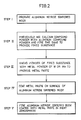
- a method of forming a metallized layer on the surface of the aforementioned aluminum nitride sintered body is performed through the following steps, in case of applying the aluminum nitride sintered body to a package for a semiconductor device etc.: Referring to Fig. 3, an aluminum nitride sintered substrate is first prepared. Then, the metal paste obtained through the aforementioned method is coated on the surface of the aluminum nitride sintered substrate. The metal paste thus coated is subjected to screen printing processing along a predetermined prescribed pattern such as a circuit pattern. The metal paste thus subjected to screen printing is thereafter dried. Then the aluminum nitride sintered substrate is fired in an inert gas atmosphere which is heated to a prescribed temperature.
- the firing step nickel plating is performed on the surface of a metallized layer formed on the aluminum nitride sintered substrate.
- Heat treatment is performed at a temperature of about 900°C to sinter the nickel plating, thereby to improve strength and airtightness of the same.
- Brazing is performed on the nickel plating surface in order to join the aluminum nitride sintered substrate with a lead frame, a heat sink member or the like. Further, gold plating is performed on such junction.
- the aluminum nitride sintered body according to the present invention can be manufactured to be applied to a substrate such as a package for a semiconductor device.
- Fig. 4A is a plan view showing an embodiment of a substrate manufactured through the aforementioned steps to be applied to a package for a semiconductor device
- Fig. 4B is a sectional view of the substrate
- Fig. 4C is a sectional view showing a junction between a lead frame 3 and an aluminum nitride substrate 1 in detail.
- the aluminum nitride substrate 1 being implemented by the inventive aluminum nitride sintered body, is partially formed on its surface with a metallized layer 2 in accordance with the present invention, and the lead frame 3 is joined to the metallized layer 2 through brazing by a brazing metal or the like.
- a semiconductor element 4 such as an FET of high calorific power is carried on a prescribed position of the package for a semiconductor device, to be connected with the metallized layer 2 or the lead frame 3 by a bonding wire 5. Further, a heat sink 6 of Cu-W alloy is mounted on the back surface of the aluminum nitride substrate 1. As shown in Fig. 4C, a plating layer 7 is formed on the metallized layer 2 in the junction between the aluminum nitride substrate 1 and the lead frame 3, while a plating layer 8 is formed at need on the surface of the lead frame 3, in order to stabilize wettability of a brazing metal 9.
- the inventive aluminum nitride sintered body can also be applied to a part of a cap for airtightly sealing a semiconductor device.
- a semiconductor element 4 is carried on an Al2O3 substrate 10.
- a cap formed by a frame 11 of Kovar (trade name of Fe-Ni29%-Co17% alloy) and an aluminum nitride sintered body 1 joined thereon is provided above the semiconductor element 4.
- the aluminum nitride sintered body 1 is formed with a metallized layer 2 on its surface closer to the frame 11.
- a compound 11a such as thermal conductive resin lies between the semiconductor element 4 and the metallized layer 2.
- a heat sink 6 is mounted on the aluminum nitride sintered body 1 to readily dissipate heat generated by the semiconductor element 4.
- the inventive aluminum nitride sintered body can be further applied to a heat sink member.
- a heat sink 6 of Cu-W alloy an aluminum nitride substrate 1 is mounted on a heat sink 6 of Cu-W alloy, and a semiconductor element 4 such as a light emitting diode (LED) or a laser diode (LD) is joined on the aluminum nitride substrate 1.
- the semiconductor element 4 is joined on a metallized layer 2 which is formed on the surface of the aluminum nitride substrate 1.
- the aluminum nitride substrate 1 serves as a heat sink member.
- the inventive aluminum nitride sintered body can also be applied to a substrate for forming an electric circuit such as a hybrid integrated circuit device or a power module.
- Fig. 7 shows an aluminum nitride substrate 1, which is applied to a submount for a semiconductor element in a hybrid semiconductor integrated circuit device (IC).
- IC hybrid semiconductor integrated circuit device
- an Al2O3 substrate 10 is formed on a copper substrate 15.
- a conductor layer 12, serving as an interconnection layer, is formed on the Al2O3 substrate 10, while a resistor 13, a capacitor 14 and the like are assembled between the same to form a circuit.
- the conductor layer 12 and the semiconductor element 4 are joined with each other by a bonding wire 5.
- the semiconductor element 4 is mounted on the copper substrate 15 through the aluminum nitride substrate 1.
- the semiconductor element 4 and the aluminum nitride substrate 1 are joined with each other through a metallized layer 2 which is formed on the surface of the aluminum nitride substrate 1.
- heat generated by the semiconductor element 4 is transferred to the aluminum nitride substrate 1, and further transmitted to the copper substrate 15 provided under the same, to be thus dissipated.
- a substrate of beryllia (BeO) is employed in place of the aluminum nitride substrate 1.
- CaO powder and Al2O3 powder were added to tungsten powder in each ratio as shown in Table 1 and kneaded with an organic binder such as vehicle to provide paste.
- Each paste thus obtained was coated on the surface of each sample prepared by an AlN sintered body and subjected to debinder processing, and thereafter fired in a nitrogen atmosphere at a temperature as shown in Table 1 for 30 minutes, to obtain a metallized layer.
- Nickel plating was performed on the metallized layer of each sample, whose tensile strength was then measured by a soldering method.
- Fig. 8 shows a method of measuring tensile strength. Referring to Fig.
- nickel plating was performed on a prescribed surface part (2 mm by 2 mm) of a metallized layer 2 which was formed on the surface of an aluminum nitride sintered body 1, and thereafter a stainless wire 16, being subjected to nickel plating of 0.8 mm ⁇ , was soldered on the same by a brazing metal 9 such as silver solder.
- the stainless wire 16 was pulled in an arrow direction, to measure the tensile strength. Table 1 also shows the results of such measurement.
- Reference example was prepared by samples fired in wet hydrogen or nitrogen and wet H2-N2 mixtured gas by employing paste similar to the above. Table 1 also shows results of measurement of tensile strength of the reference example.
- Airtightness of the metallized layer in each sample was examined by an He detector. All of the samples fired in accordance with the present invention were excellent in airtightness, while the reference samples were extremely inferior in airtightness. Within reference example, the sample No. 5 of tungsten paste was fired in nitrogen, and the remaining samples were fired in wet hydrogen or nitrogen and wet H2-N2 mixtured gas.
- AlN sintered bodies having metallized layers were prepared similarly to Example 1, except for that CaO was replaced by CaCO3 or Ca(NO3)2.
- the firing condition was one hour under a temperature of 1600°C.
- Table 2 shows results of tensile strength of the samples thus obtained measured similarly to Example 1. It is obvious from Table 2 that the metallized layers formed in accordance with the present invention were excellent in junction strength, similarly to Example 1. Further, the samples of Example 2 were also excellent in airtightness, which was measured similarly to Example 1.
- CaO powder and AlN powder were added to tungsten powder in each ratio as shown in Table 3 and kneaded with an organic binder such as vehicle to provide paste.
- Each paste thus obtained was coated on the surface of each sample prepared by an AlN sintered body and subjected to debinder processing, and thereafter fired in a nitrogen atmosphere at a temperature as shown in Table 3 for 60 minutes, to obtain a metallized layer.
- the metallized layer of each sample was subjected to nickel plating, and tensile strength thereof was measured similarly to Example 1. Table 3 shows the results of such measurement.
- Reference example was prepared by samples fired in wet hydrogen or nitrogen and wet H2-N2 mixtured gas through employment of paste similar to the above.
- Table 3 also shows the results of tensile strength of each reference sample measured in a similar manner to the above.
- Airtightness of each sample was examined by an He detector. All of the samples fired in accordance with the present invention were excellent in airtightness, while all of the reference samples were extremely inferior in airtightness.
- the sample No. 5 of tungsten paste was fired in nitrogen and the remaining samples were fired in wet hydrogen or nitrogen and wet H2-N2 mixtured gas.
- AlN sintered bodies having metallized layers were prepared similarly to Example 3, except for that CaO was replaced by CaCO3 or Ca(NO3)2.
- the firing condition was 120 minutes under a temperature of 1700°C.
- Table 4 shows tensile strength of each sample thus obtained, which was measured similarly to Example 1. It is obvious from Table 4 that all of the metallized layers formed in accordance with the present invention were excellent in junction strength. The samples of Example 4 were also excellent in airtightness, which was measured in a similar manner to Example 3.
- Each paste thus obtained was coated on the surface of each sample prepared by an AlN sintered body and subjected to debinder processing, and thereafter fired in a nitrogen atmosphere at a temperature of 1600°C for 60 minutes, to obtain a metallized layer.
- the metallized layer of each sample was subjected to nickel plating of 2 to 3 ⁇ m in thickness and further subjected to gold plating of 2 to 3 ⁇ m in thickness, and thereafter heat treatment was performed in the atmosphere at a temperature of 450°C for 10 minutes, to examine the status of tarnishing and foaming on the plating surface.
- Table 5 shows the results. Further, appearance inspection was performed by a stereomicroscope of forty magnifications. Symbol A in Table 5 indicates those whose plating surfaces were recognized to be tarnished or foamed in the ratio of 0 to 5 % within 100 samples, symbol B indicates those in the ratio of 5 to 10 % and symbol C indicates those in the ratio of at least 10 %.
- a metallized layer of each composition as shown in Table 5 was formed on the surface of each sample prepared by an AlN sintered body having a prescribed configuration, and a nickel plating layer of 2 to 3 ⁇ m in thickness and a gold plating layer of 2 to 3 ⁇ m in thickness were formed on the same. Thereafter a field-effect high-power transistor was soldered/carried on the surface of the plating layer by a brazing filler metal of Au-Si. A ⁇ V BE method was performed to measure change ⁇ V BE in forward voltage drop V BE across the emitter and the base of the transistor caused by electric power application, thereby to evaluate thermal resistance of the integrated transistor and AlN sintered body. Table 5 also shows the thermal resistance value of each sample.
- Fig. 9B illustrates thermal resistance of each sample integrated with the transistor obtained in Example 5, in terms of relation to contents of Al2O3 and CaO. Referring to Figs. 9A and 9B, numeric values in parentheses represent tensile strength and thermal resistance values respectively.
- each metallized layer containing 1 to 5 percent by weight of aluminum oxide and 1 to 15 percent by weight of calcium oxide had a small degree of tarnishing frequency of gold plating. It is recognized that the plating layer formed on the metallized layer was particularly excellent in adhesive property with the contents of such ranges. Further, it is recognized from Fig. 9A that each metallized layer containing 1 to 10 percent by weight of aluminum oxide and 10 to 20 percent by weight of calcium oxide had junction strength, being evaluated as tensile strength, of at least about 7 Kg/mm2, to implement an aluminum nitride sintered body which is preferably applied to a part of a package substrate for a semiconductor device. According to Fig.
- each AlN sintered body being integrated with a transistor, having a metallized layer containing 1 to 10 percent by weight of aluminum oxide and 3 to 15 percent by weight of calcium oxide had a thermal resistance value of not more than about 1.9°C/W, to implement an AlN sintered body which is suitable for forming a part of a heat sink for a semiconductor device.
- Reference example was formed by firing tungsten paste materials independently containing 7 percent by weight of borosilicate glass, 15 percent by weight of CaO and 8 percent by weight of Al2O3 respectively as assistants in a nitrogen atmosphere and a wet atmosphere similarly to Example 5. Tensile strength of each metallized layer thus obtained was unmeasurable and by far different from a practical level. Further, paste identical in composition to that of Example 5 was fired in a wet atmosphere. Thermal resistance of an AlN sintered body having the metallized layer thus obtained was in excess of 2.5°C/W through measurement in a similar manner to the above.
- Example 5 CaO powder and Al2O3 powder were added to molybdenum powder in each ratio as shown in Table 6 and kneaded with an organic binder such as vehicle, to provide paste.
- Each paste thus obtained was coated on the surface of each sample prepared by an AlN sintered body and subjected to debinder processing, and thereafter fired in a nitrogen atmosphere at a temperature of 1550°C for 30 minutes, to obtain a metallized layer.
- a nickel plating layer of 2 to 3 ⁇ m in thickness and a gold plating layer of 2 to 3 ⁇ m in thickness were formed on the metallized layer of each sample, which was then subjected to heat treatment in the atmosphere at a temperature of 450°C for 10 minutes, to examine the status of tarnishing and foaming on the plating surface.
- Table 6 shows the results of such examination, similarly to Example 5.
- Table 6 also shows the result of measurement of tensile strength of each sample, similarly to Example 5.
- Example 6 shows the result of measurement of thermal resistance with respect to each sample.
- Fig. 10A illustrates measured values of tensile strength thus obtained in terms of relation to contents of Al2O3 and CaO.
- Fig. 10B illustrates thermal resistance values in terms of relation to the contents of Al2O3 and CaO. Numeric values in the parentheses show tensile strength values and thermal resistance values in Figs. 10A and 10B respectively.
- each metallized layer containing 1 to 5 percent by weight of aluminum oxide and 1 to 25 percent by weight of calcium oxide had small tarnishing frequency of gold plating, and was excellent in plating adhesive property.
- each metallized layer containing 1 to 10 percent by weight of aluminum oxide and 15 to 35 percent by weight of calcium oxide shows junction strength, being evaluated as tensile strength, of at least about 7 Kg/mm2, to implement an AlN sintered body which is preferably applied to a part of a substrate of a package for a semiconductor device requiring excellent junction strength.
- each AlN sintered body having a metallized layer containing 1 to 7 percent by weight of aluminum oxide and 1 to 35 percent by weight of calcium oxide shows a thermal resistance value of not more than about 3.0°C/W in integration with a transistor, to implement an AlN sintered body which is preferably applied to a part requiring good thermal conductivity.
- Reference example was formed by firing molybdenum paste materials independently containing 14 percent by weight of borosilicate glass, 18 percent by weight of CaO and 7 percent by weight of Al2O3 respectively as assistants in a nitrogen atmosphere and a wet atmosphere similarly to Example 6. Tensile strength of each metallized layer thus obtained was unmeasurable and by far different from a practical level. Further, paste being identical in composition to that in Example 6 was fired in a wet atmosphere to obtain a metallized layer. Thermal resistance of an AlN sintered body provided with this metallized layer was in excess of 3.5°C/W, as the result of measurement performed similarly to the above.
- Calcium nitrate powder and aluminum oxide powder were fully mixed in the ratio of 30 g to 5 g, and fired in the air at a temperature of 1350°C for three hours.
- the fired substance thus obtained was a mixture of xCaO ⁇ yAl2O3 (x,y: an integer) and CaO, which was then pulverized by a ball mill. 30 percent by weight of the powder thus obtained was blended with 70 percent by weight of molybdenum powder, and an organic binder such as vehicle was added to the same thereby to provide molybdenum paste.
- the molybdenum paste was screen-printed on the surface of an AlN sintered body in a pattern having an area of 2 mm by 2 mm, and then fired in a nitrogen atmosphere at each firing temperature as shown in Table 7 for 120 minutes.
- Nickel plating was performed on the surface of each metallized layer thus obtained, to measure tensile strength similarly to Example 1. After the nickel plating, gold plating was further performed and a field-effect high-power transistor was carried on the same similarly to Example 5, to measure thermal resistance. Table 7 shows the results of such measurement.
- each aluminum compound was prepared by aluminum oxide or aluminum nitride in the aforementioned Examples, a similar function/effect can be attained by employing aluminum oxynitride.
- a metallized layer which is strongly adhered to an aluminum nitride sintered body, can be obtained with high airtightness and excellent thermal conductivity. Further, according to the inventive manufacturing method, firing of metal paste coated on an aluminum nitride sintered body can be performed in an inert atmosphere.
Landscapes
- Chemical & Material Sciences (AREA)
- Engineering & Computer Science (AREA)
- Ceramic Engineering (AREA)
- Inorganic Chemistry (AREA)
- Materials Engineering (AREA)
- Structural Engineering (AREA)
- Organic Chemistry (AREA)
- Ceramic Products (AREA)
- Cooling Or The Like Of Semiconductors Or Solid State Devices (AREA)
Applications Claiming Priority (4)
| Application Number | Priority Date | Filing Date | Title |
|---|---|---|---|
| JP16422/87 | 1987-01-26 | ||
| JP1642287 | 1987-01-26 | ||
| JP16421/87 | 1987-01-26 | ||
| JP1642187 | 1987-01-26 |
Publications (3)
| Publication Number | Publication Date |
|---|---|
| EP0276788A2 true EP0276788A2 (fr) | 1988-08-03 |
| EP0276788A3 EP0276788A3 (en) | 1989-05-31 |
| EP0276788B1 EP0276788B1 (fr) | 1993-01-13 |
Family
ID=26352765
Family Applications (1)
| Application Number | Title | Priority Date | Filing Date |
|---|---|---|---|
| EP88101015A Expired - Lifetime EP0276788B1 (fr) | 1987-01-26 | 1988-01-25 | Corps fritté en nitrure d'aluminium ayant une couche métallisée et son procédé de fabrication |
Country Status (4)
| Country | Link |
|---|---|
| EP (1) | EP0276788B1 (fr) |
| KR (1) | KR930005894B1 (fr) |
| CA (1) | CA1333241C (fr) |
| DE (1) | DE3877370T2 (fr) |
Cited By (8)
| Publication number | Priority date | Publication date | Assignee | Title |
|---|---|---|---|---|
| EP0390598A3 (fr) * | 1989-03-31 | 1991-06-12 | Kabushiki Kaisha Toshiba | Substrat en nitride d'aluminium métallisé |
| EP0433992A1 (fr) * | 1989-12-20 | 1991-06-26 | Sumitomo Electric Industries, Ltd. | Procédé de formation d'une couche métallisée sur un corps fritté de nitrure d'aluminium |
| EP0515061A1 (fr) * | 1991-05-21 | 1992-11-25 | Fujitsu Limited | Procédé pour la fabrication d'un panneau de circuit multi-couche en nitrure d'aluminium |
| EP0463872A3 (en) * | 1990-06-29 | 1993-02-03 | Kabushiki Kaisha Toshiba | Method of manufacturing circuit board and circuit board itself manufactured by said method |
| EP0529752A3 (en) * | 1991-08-22 | 1993-03-31 | W.R. Grace & Co.-Conn. | Via metallization for a1n ceramic electronic package |
| US5292552A (en) * | 1989-12-20 | 1994-03-08 | Sumitomo Electric Industries, Ltd. | Method for forming metallized layer on an aluminum nitride sintered body |
| EP0737657A3 (fr) * | 1995-04-13 | 1997-04-23 | Hoechst Ceram Tec Ag | Procédé pour la fabrication d'un composant métallisé à revêtement métallique à base de céramique en nitrure d'aluminium et le composant à revêtement métallique ainsi obtenu |
| CN119461893A (zh) * | 2024-11-25 | 2025-02-18 | 哈尔滨工业大学(威海) | 一种激光表面改性技术用于连接陶瓷/玻璃与金属的方法 |
Families Citing this family (1)
| Publication number | Priority date | Publication date | Assignee | Title |
|---|---|---|---|---|
| WO2006051881A1 (fr) * | 2004-11-12 | 2006-05-18 | Tokuyama Corporation | Procede de fabrication d'un substrat en nitrure d'aluminium metallise et substrat ainsi obtenu |
Family Cites Families (3)
| Publication number | Priority date | Publication date | Assignee | Title |
|---|---|---|---|---|
| US4695517A (en) * | 1985-05-31 | 1987-09-22 | Ngk Spark Plug Co., Ltd. | Composite layer aluminum nitride base sintered body |
| JPS6265991A (ja) * | 1985-09-13 | 1987-03-25 | 株式会社東芝 | 高熱伝導性セラミツクス基板 |
| EP0235682B2 (fr) * | 1986-02-20 | 1997-11-12 | Kabushiki Kaisha Toshiba | Corps frité à base de nitrure d'aluminium, muni d'une couche métallisée conductrice |
-
1988
- 1988-01-22 CA CA000557216A patent/CA1333241C/fr not_active Expired - Lifetime
- 1988-01-25 EP EP88101015A patent/EP0276788B1/fr not_active Expired - Lifetime
- 1988-01-25 DE DE8888101015T patent/DE3877370T2/de not_active Expired - Lifetime
- 1988-01-25 KR KR1019880000531A patent/KR930005894B1/ko not_active Expired - Lifetime
Cited By (13)
| Publication number | Priority date | Publication date | Assignee | Title |
|---|---|---|---|---|
| US5637406A (en) * | 1989-03-31 | 1997-06-10 | Kabushiki Kaisha Toshiba | Metallized aluminum nitride substrate |
| EP0390598A3 (fr) * | 1989-03-31 | 1991-06-12 | Kabushiki Kaisha Toshiba | Substrat en nitride d'aluminium métallisé |
| US5292552A (en) * | 1989-12-20 | 1994-03-08 | Sumitomo Electric Industries, Ltd. | Method for forming metallized layer on an aluminum nitride sintered body |
| EP0433992A1 (fr) * | 1989-12-20 | 1991-06-26 | Sumitomo Electric Industries, Ltd. | Procédé de formation d'une couche métallisée sur un corps fritté de nitrure d'aluminium |
| EP0463872A3 (en) * | 1990-06-29 | 1993-02-03 | Kabushiki Kaisha Toshiba | Method of manufacturing circuit board and circuit board itself manufactured by said method |
| US5286927A (en) * | 1990-06-29 | 1994-02-15 | Kabushiki Kaisha Toshiba | Method of manufacturing circuit board and circuit board itself manufactured by said method |
| EP0515061A1 (fr) * | 1991-05-21 | 1992-11-25 | Fujitsu Limited | Procédé pour la fabrication d'un panneau de circuit multi-couche en nitrure d'aluminium |
| US5683529A (en) * | 1991-05-21 | 1997-11-04 | Fujitsu Limited | Process of producing aluminum nitride multiple-layer circuit board |
| EP0529752A3 (en) * | 1991-08-22 | 1993-03-31 | W.R. Grace & Co.-Conn. | Via metallization for a1n ceramic electronic package |
| EP0737657A3 (fr) * | 1995-04-13 | 1997-04-23 | Hoechst Ceram Tec Ag | Procédé pour la fabrication d'un composant métallisé à revêtement métallique à base de céramique en nitrure d'aluminium et le composant à revêtement métallique ainsi obtenu |
| US5856028A (en) * | 1995-04-13 | 1999-01-05 | Hoechst Ceramtec Ag | Process for producing a metal-coated, metallized component of aluminum nitride ceramic and metal-coated component obtained thereby |
| US6077564A (en) * | 1995-04-13 | 2000-06-20 | Hoechst Ceramtec Ag | Process for producing a metal-coated, metallized component of aluminum nitride ceramic and metal-coated component obtained thereby |
| CN119461893A (zh) * | 2024-11-25 | 2025-02-18 | 哈尔滨工业大学(威海) | 一种激光表面改性技术用于连接陶瓷/玻璃与金属的方法 |
Also Published As
| Publication number | Publication date |
|---|---|
| DE3877370T2 (de) | 1993-05-06 |
| EP0276788B1 (fr) | 1993-01-13 |
| KR930005894B1 (ko) | 1993-06-25 |
| DE3877370D1 (de) | 1993-02-25 |
| KR880009138A (ko) | 1988-09-14 |
| CA1333241C (fr) | 1994-11-29 |
| EP0276788A3 (en) | 1989-05-31 |
Similar Documents
| Publication | Publication Date | Title |
|---|---|---|
| US5529852A (en) | Aluminum nitride sintered body having a metallized coating layer on its surface | |
| US4965659A (en) | Member for a semiconductor structure | |
| EP0297569B1 (fr) | Support pour appareil semi-conducteur | |
| EP0153737B1 (fr) | Substrat pour circuit à haute thermoconductivité | |
| EP0297511B1 (fr) | Structure de connexion entre des composants pour appareil semi-conducteur | |
| US5033666A (en) | Process for brazing metallized components to ceramic substrates | |
| KR100328407B1 (ko) | 세라믹회로기판 | |
| US4695517A (en) | Composite layer aluminum nitride base sintered body | |
| Iwase et al. | Thick film and direct bond copper forming technologies for aluminum nitride substrate | |
| KR900005842B1 (ko) | 질화 알루미늄 기판 | |
| KR910000336B1 (ko) | 전자기기 장치 | |
| EP0452871A1 (fr) | Corps fritté en nitrure d'aluminium ayant conductibilité thermique et coloration et procédé de sa fabrication | |
| EP0276788B1 (fr) | Corps fritté en nitrure d'aluminium ayant une couche métallisée et son procédé de fabrication | |
| JPH06296084A (ja) | 高熱伝導体及びこれを備えた配線基板とこれらの製造方法 | |
| US4941582A (en) | Hermetically sealed ceramic package | |
| Kurihara et al. | Ag-Pd thick film conductor for AlN ceramics | |
| US4963187A (en) | Metallizing paste for circuit board having low thermal expansion coefficient | |
| JP2523162B2 (ja) | 半導体装置用部材 | |
| EP0433992B1 (fr) | Procédé de formation d'une couche métallisée sur un corps fritté de nitrure d'aluminium | |
| JPS61248302A (ja) | 炭化ケイ素焼結体用メタライズペ−スト | |
| JP2650044B2 (ja) | 半導体装置用部品間の接続構造 | |
| US5292552A (en) | Method for forming metallized layer on an aluminum nitride sintered body | |
| JPS63303881A (ja) | 金属化層が形成された窒化アルミニウム焼結体およびその製造方法 | |
| JPH0748180A (ja) | セラミックス−金属接合体 | |
| US5830570A (en) | Aluminum nitride substrate and process for preparation thereof |
Legal Events
| Date | Code | Title | Description |
|---|---|---|---|
| PUAI | Public reference made under article 153(3) epc to a published international application that has entered the european phase |
Free format text: ORIGINAL CODE: 0009012 |
|
| AK | Designated contracting states |
Kind code of ref document: A2 Designated state(s): DE FR GB IT |
|
| PUAL | Search report despatched |
Free format text: ORIGINAL CODE: 0009013 |
|
| AK | Designated contracting states |
Kind code of ref document: A3 Designated state(s): DE FR GB IT |
|
| 17P | Request for examination filed |
Effective date: 19890613 |
|
| RAP1 | Party data changed (applicant data changed or rights of an application transferred) |
Owner name: SUMITOMO ELECTRIC INDUSTRIES, LIMITED |
|
| 17Q | First examination report despatched |
Effective date: 19910308 |
|
| GRAA | (expected) grant |
Free format text: ORIGINAL CODE: 0009210 |
|
| AK | Designated contracting states |
Kind code of ref document: B1 Designated state(s): DE FR GB IT |
|
| REF | Corresponds to: |
Ref document number: 3877370 Country of ref document: DE Date of ref document: 19930225 |
|
| ITF | It: translation for a ep patent filed | ||
| ET | Fr: translation filed | ||
| PLBE | No opposition filed within time limit |
Free format text: ORIGINAL CODE: 0009261 |
|
| STAA | Information on the status of an ep patent application or granted ep patent |
Free format text: STATUS: NO OPPOSITION FILED WITHIN TIME LIMIT |
|
| 26N | No opposition filed | ||
| REG | Reference to a national code |
Ref country code: GB Ref legal event code: IF02 |
|
| PGFP | Annual fee paid to national office [announced via postgrant information from national office to epo] |
Ref country code: DE Payment date: 20070118 Year of fee payment: 20 |
|
| PGFP | Annual fee paid to national office [announced via postgrant information from national office to epo] |
Ref country code: GB Payment date: 20070124 Year of fee payment: 20 |
|
| PGFP | Annual fee paid to national office [announced via postgrant information from national office to epo] |
Ref country code: IT Payment date: 20070622 Year of fee payment: 20 |
|
| REG | Reference to a national code |
Ref country code: GB Ref legal event code: PE20 |
|
| PGFP | Annual fee paid to national office [announced via postgrant information from national office to epo] |
Ref country code: FR Payment date: 20070109 Year of fee payment: 20 |
|
| PG25 | Lapsed in a contracting state [announced via postgrant information from national office to epo] |
Ref country code: GB Free format text: LAPSE BECAUSE OF EXPIRATION OF PROTECTION Effective date: 20080124 |