EP0276850A2 - Integrierte Halbleiterschaltung mit Struktur gegen Verriegelung - Google Patents
Integrierte Halbleiterschaltung mit Struktur gegen Verriegelung Download PDFInfo
- Publication number
- EP0276850A2 EP0276850A2 EP88101237A EP88101237A EP0276850A2 EP 0276850 A2 EP0276850 A2 EP 0276850A2 EP 88101237 A EP88101237 A EP 88101237A EP 88101237 A EP88101237 A EP 88101237A EP 0276850 A2 EP0276850 A2 EP 0276850A2
- Authority
- EP
- European Patent Office
- Prior art keywords
- region
- power source
- potential
- integrated circuit
- semiconductor integrated
- Prior art date
- Legal status (The legal status is an assumption and is not a legal conclusion. Google has not performed a legal analysis and makes no representation as to the accuracy of the status listed.)
- Withdrawn
Links
Images


Classifications
-
- H—ELECTRICITY
- H10—SEMICONDUCTOR DEVICES; ELECTRIC SOLID-STATE DEVICES NOT OTHERWISE PROVIDED FOR
- H10D—INORGANIC ELECTRIC SEMICONDUCTOR DEVICES
- H10D84/00—Integrated devices formed in or on semiconductor substrates that comprise only semiconducting layers, e.g. on Si wafers or on GaAs-on-Si wafers
- H10D84/80—Integrated devices formed in or on semiconductor substrates that comprise only semiconducting layers, e.g. on Si wafers or on GaAs-on-Si wafers characterised by the integration of at least one component covered by groups H10D12/00 or H10D30/00, e.g. integration of IGFETs
- H10D84/82—Integrated devices formed in or on semiconductor substrates that comprise only semiconducting layers, e.g. on Si wafers or on GaAs-on-Si wafers characterised by the integration of at least one component covered by groups H10D12/00 or H10D30/00, e.g. integration of IGFETs of only field-effect components
- H10D84/83—Integrated devices formed in or on semiconductor substrates that comprise only semiconducting layers, e.g. on Si wafers or on GaAs-on-Si wafers characterised by the integration of at least one component covered by groups H10D12/00 or H10D30/00, e.g. integration of IGFETs of only field-effect components of only insulated-gate FETs [IGFET]
- H10D84/85—Complementary IGFETs, e.g. CMOS
- H10D84/854—Complementary IGFETs, e.g. CMOS comprising arrangements for preventing bipolar actions between the different IGFET regions, e.g. arrangements for latchup prevention
-
- H—ELECTRICITY
- H10—SEMICONDUCTOR DEVICES; ELECTRIC SOLID-STATE DEVICES NOT OTHERWISE PROVIDED FOR
- H10D—INORGANIC ELECTRIC SEMICONDUCTOR DEVICES
- H10D84/00—Integrated devices formed in or on semiconductor substrates that comprise only semiconducting layers, e.g. on Si wafers or on GaAs-on-Si wafers
- H10D84/01—Manufacture or treatment
- H10D84/0123—Integrating together multiple components covered by H10D12/00 or H10D30/00, e.g. integrating multiple IGBTs
- H10D84/0126—Integrating together multiple components covered by H10D12/00 or H10D30/00, e.g. integrating multiple IGBTs the components including insulated gates, e.g. IGFETs
- H10D84/0165—Integrating together multiple components covered by H10D12/00 or H10D30/00, e.g. integrating multiple IGBTs the components including insulated gates, e.g. IGFETs the components including complementary IGFETs, e.g. CMOS devices
- H10D84/0191—Manufacturing their doped wells
-
- H—ELECTRICITY
- H10—SEMICONDUCTOR DEVICES; ELECTRIC SOLID-STATE DEVICES NOT OTHERWISE PROVIDED FOR
- H10D—INORGANIC ELECTRIC SEMICONDUCTOR DEVICES
- H10D89/00—Aspects of integrated devices not covered by groups H10D84/00 - H10D88/00
- H10D89/60—Integrated devices comprising arrangements for electrical or thermal protection, e.g. protection circuits against electrostatic discharge [ESD]
- H10D89/601—Integrated devices comprising arrangements for electrical or thermal protection, e.g. protection circuits against electrostatic discharge [ESD] for devices having insulated gate electrodes, e.g. for IGFETs or IGBTs
- H10D89/711—Integrated devices comprising arrangements for electrical or thermal protection, e.g. protection circuits against electrostatic discharge [ESD] for devices having insulated gate electrodes, e.g. for IGFETs or IGBTs using bipolar transistors as protective elements
-
- H—ELECTRICITY
- H10—SEMICONDUCTOR DEVICES; ELECTRIC SOLID-STATE DEVICES NOT OTHERWISE PROVIDED FOR
- H10D—INORGANIC ELECTRIC SEMICONDUCTOR DEVICES
- H10D89/00—Aspects of integrated devices not covered by groups H10D84/00 - H10D88/00
- H10D89/60—Integrated devices comprising arrangements for electrical or thermal protection, e.g. protection circuits against electrostatic discharge [ESD]
- H10D89/601—Integrated devices comprising arrangements for electrical or thermal protection, e.g. protection circuits against electrostatic discharge [ESD] for devices having insulated gate electrodes, e.g. for IGFETs or IGBTs
- H10D89/811—Integrated devices comprising arrangements for electrical or thermal protection, e.g. protection circuits against electrostatic discharge [ESD] for devices having insulated gate electrodes, e.g. for IGFETs or IGBTs using FETs as protective elements
Definitions
- This invention relates to a complementary MOS semiconductor integrated circuit device, and more particularly to a semiconductor integrated circuit device which can be made effectively free from latch-up at the time of introduction of surge from a power source terminal.
- the latch-up phenomenon occurs at the time of generation of surge not only at a signal output terminal but also at a signal input terminal because of, for example, a diode connected to the input terminal for input protection.
- CMOS TECHNOLOGY OPTIONS T. BATRA et al. American Microsystems, Inc. 3800 Homestead road Santa Clara, CA 95051 IEEE 1982
- a countermeasure is taken by, for example, enhancing the substrate bias at portions near the signal input and output terminals so that the surge may be absorbed into the power source terminal, thus preventing the introduced surge from being transmitted to internal elements.
- the latch-up preventing characteristic with respect to the surge introduced at the power source terminal becomes worse than that with respect to the surge introduced at the other terminal.
- the latch-up phenomenon may easily occur when a surge is introduced via the power source terminal.
- This invention has been made in view of the fact described above, and an object thereof is to provide a semiconductor integrated circuit device having an improved latch-up preventing characteristic with respect to an external surge introduced via a power source.
- a semiconductor integrated circuit device includes a MOS transistor (13) having source and gate electrodes connected to a first node (N1) to which a first power source potential (VDD) is applied and a drain electrode connected to a second node to which a second power source potential (GND) is applied.
- MOS transistor (13) having source and gate electrodes connected to a first node (N1) to which a first power source potential (VDD) is applied and a drain electrode connected to a second node to which a second power source potential (GND) is applied.
- the MOS transistor (13) is kept in the off state in an ordinary operation state in which no surge is generated at the first and second nodes (N1, N2). Therefore, in this case, the MOS transistor (13) is set nonoperative.
- VN a potential difference between the gate and drain electrodes of the MOS transistor (13) which are respectively connected to the first and second nodes (N1, N2) exceeds the threshold voltage (VTH) of the MOS transistor (13)
- VTH threshold voltage
- the MOS transistor (13) is turned on. This creates a current path from the second node (N2) to the first node (N1), thus permitting a surge applied to one of the nodes (N2) to be absorbed in the other node (N1).
- the parasitic bipolar transistor When the source or drain voltage of the MOS transistor (13) rises and if a base current flows into a parasitic PNP or NPN bipolar transistor whose emitter and collector are formed of the source and drain regions of the MOS transistor (13), the parasitic bipolar transistor is turned on. Then, a current path is created between the first and second nodes (N1, N2) due to the collector current flow of the parasitic bipolar transistor, causing a surge applied to one of the first and second nodes (e.g., N2) to be absorbed into the other node (N1). Further, in the case where a large current surge is applied, a collector current flowing in the parasitic bipolar transistor acts as a main surge current.
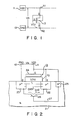
- Fig. 1 is a circuit diagram showing the construction of a first embodiment of this invention.
- Fig. 1 denotes an external connection terminal of the IC to which a high potential or VDD potential, for example, +5V, is applied, and 12 denotes an external connection terminal to which a low potential or GND potential (0 V) is applied.
- VDD potential for example, +5V
- GND potential 0 V
- the source and gate electrodes of enhancement type P channel MOS transistor 13 are connected to VDD terminal 11
- the drain electrode of MOS transistor 13 is connected to GND terminal 12.
- a substrate or the back gate electrode of MOS transistor 13 is connected to terminal 11.
- Fig. 2 is a cross-sectional view showing the construction of a device obtained when the Fig. 1 circuit is formed in an integrated circuit form.
- 21 denotes N-type substrate; 22 and 23, P+-type source and drain regions formed in N-type substrate 21; 24, a gate electrode; and 25, an N+-type region formed for substrate bias in order to apply a VDD potential to substrate 21.
- Gate electrode 24 is placed over a channel between regions 22 and 23, via gate oxide layer (SiO2) 70.
- parasitic PNP transistor 26 having source region 22, drain region 23, and substrate 21, respectively serving as a collector, emitter, and base, is formed in substrate 21. Further, parasitic resistor 27 formed of a resistive component of substrate 21 is connected between the base of parasitic PNP transistor 26 and N+-type region 25. Whether the collector and emitter of parasitic PNP transistor 26 are respectively formed of regions 22 and 23, or regions 23 and 22, is determined by the relation between potentials of regions 22 and 23.
- the potential of source region 22 of transistor 13 is also lowered with decrease in the VDD potential. At this time, the potential of substrate 21 will not change so rapidly as the potential of source region 22 due to the presence of resistor 27.
- V B breakdown voltage
- a breakdown current begins to flow from substrate 21 to source region 22. This causes the potential of substrate 21 to be lowered and the substrate potential tends to approach the source potential which has already been lowered.
- a PN junction current begins to flow from drain region 23 to substrate 21.
- This current is supplied to parasitic PNP transistor 26 as the base current so as to turn on transistor 26, causing collector current icol to flow, as is shown in Fig. 2.
- a PN junction current begins to flow from drain region 23 to substrate 21.
- the current is supplied as a base current to parasitic PNP transistor 26 to turn on transistor 26, causing collector current icol to flow as shown in Fig. 2.
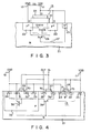
- Fig. 4 is a cross-sectional view of a semiconductor circuit device having a CMOS inverter circuit together with the circuit of Fig. 1.
- 30 denotes a P-type well region formed in an N-type substrate; 31 and 32, source and drain regions of an N channel MOS transistor constituting the CMOS inverter circuit and formed in P-type well (P-well) region 30; 33, a gate electrode of the transistor; 34, a biasing P+-type region for supplying a GND potential to P-type well region 30; 35 and 36, source and drain regions of a P channel MOS transistor constituting the CMOS inverter circuit and formed in N-type substrate 21; and 37, a gate electrode of the transistor.
- a parasitic thyristor will be formed to include parasitic NPN transistor 38, having an emitter, base and collector respectively formed of N+-type region 31, P-type well region 30 and N-type substrate 21, and parasitic PNP transistor 39, having an emitter, base and collector respectively formed of P+-type region 36, N-type substrate 21 and P-type well region 30.
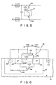
- Fig. 5 is a circuit diagram showing the construction of a second embodiment of this invention.
- 11 and 12 denote external connection terminals to which a VDD potential (high potential) and a GND potential are respectively applied.
- terminal 11 is connected to a drain electrode of enhancement type N channel MOS transistor 14.
- Source and gate electrodes of transistor 14 are connected to terminal 12. Further, a substrate or the back gate electrode of transistor 13 is also connected to terminal 12.
- Fig. 6 is a cross-sectional view showing the construction of an integrated circuit including a P-type well region to form the circuit of Fig. 5.
- 41 denotes an N-type substrate
- 42 a P-type well region formed in substrate 41
- 43 and 44 N+-type source and drain regions of N channel MOS transistor 14 formed in P-type well region 42
- 45 a gate electrode of the transistor
- 46 a biasing P+-type region for setting P-type well region 42 to the GND potential
- 47 a biasing N+-type region for setting N-type substrate 41 to the VDD potential.
- parasitic NPN bipolar transistor 48 having a collector, emitter and base formed of N+-type source and drain regions 43 and 44 and P-type well region 42 is created in P-type well region 42. Further, parasitic resistor 49 formed of resistance component of P-type well region 42 is connected between region 46 and the base of parasitic bipolar transistor 48. In the case, whether the emitter and collector of parasitic NPN transistor 48 are respectively formed of regions 43 and 44, or regions 44 and 43 is determined according to the potential relation between regions 43 and 44.
- a PN junction current begins to flow from P-type well region 42 to drain region 44.
- the current is supplied to parasitic bipolar transistor 48 as the base current to turn on transistor 48, causing collector current icol to flow as shown in Fig. 6.
- the GND potential falls and the potential of source region 43 falls.
- the source potential becomes lower than the potential of P-type well region 42 by forward voltage VF of the PN junction between regions 42 and 43, a forward current starts to flow from P-type well region 42 to source region 43 via the PN junction.
- the current is supplied as a base current to NPN transistor 48 to turn on transistor 48, causing collector current icol* to flow in a direction as shown in Fig. 7.
- Fig. 8 is a cross-sectional view of a semiconductor circuit device having a CMOS inverter circuit together with the circuit of the above embodiment.
- 51 and 52 denote source and drain regions of an N channel MOS transistor constituting the CMOS inverter circuit and formed in P-type well region 42; 53, a gate electrode of the transistor; 54 and 55, source and drain regions of a P channel MOS transistor constituting the CMOS inverter circuit and formed in N-type substrate 41; 56, a gate electrode of the transistor; and 57, a biasing N+-type region for setting N-type substrate 41 to the VDD potential.
- a parasitic thyristor will be formed to include parasitic NPN transistor 58, having an emitter, base and collector respectively formed of N+-type region 51, P-type well region 42 and N-type substrate 41, and parasitic PNP transistor 59, having an emitter, base and collector respectively formed of P+-type region 54, N-type substrate 41 and P-type well region 42.
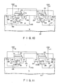
- Fig. 9 is a circuit diagram showing the construction of a third embodiment of this invention.
- P channel MOS transistor 13 in the circuit of the first embodiment and N channel MOS transistor 14 in the circuit of the second embodiment are used.
- Figs. 10 and 11 are cross-sectional views showing the construction of a device obtained when the Fig. 9 circuit is formed in the form of integrated circuit utilizing a P-type well region.
- Fig. 10 shows the cases (1) and (2)
- Fig. 11 shows the cases (3) and (4).
- 21 denotes N-type substrate; 22 and 23, P+-type source and drain regions formed in N-type substrate 21; 24, an gate electrode; and 25, an N+-type region for applying a VDD potential to substrate 21.
- parasitic PNP transistor 26 is formed to have source and drain regions 22 and 23 and substrate 21 as a collector, emitter and base.
- 27 denotes a parasitic resistor
- 42 P-type well region formed in substrate 21; 43 and 44, N+-type source and drain regions of N channel MOS transistor 14 formed in P-type well region 42; 45, a gate electrode of the transistor; 46, a biasing P+-type region for setting P-type well region 42 to the GND potential; 48, a parasitic NPN bipolar transistor having a collector, emitter and base formed of N+-type source and drain regions 43 and 44 and P-type well region 42; and 49, a parasitic resistor formed of resistance component of P-type well region 42.
- the ability of absorbing the surge into the power source terminal can be more enhanced in comparison with the circuits of the first and second embodiments, because two current paths are formed on both the N and P channel circuits between terminals 11 and 12. Therefore, the surge can be absorbed into the power source in a brief time, thereby greatly improving the latch-up preventing characteristic.
- Fig. 12 shows currents flowing in transistors 13 and 14 in the circuit of the embodiment in Fig. 9 when a surge is applied to terminal 11 or 12.
- "o" mark indicates that a current flows
- "x” mark indicates that no current flows.
- a negative surge is applied to the VDD terminal, a channel current, collector current and punch-through current flow in P channel MOS transistor 13, and a channel current and collector current flow in N channel MOS transistor 14.
- Figs. 13 and 14 are circuit diagrams showing the constructions of test circuits for checking whether or not the latch-up phenomenon occurs when a surge is applied to the power source of a CMOS-IC according to this invention in which P channel MOS transistor 13 and N channel MOS transistor 14 are both formed as shown in Fig. 9.
- Fig. 13 shows the test circuit for applying a surge to the VDD terminal, and VDD and GND potentials are externally supplied to terminals 11 and 12 of CMOS-IC 60, respectively.
- switch 61 is first closed to charge capacitor 63 with a capacitance of, for example, 200 pF by means of power source 62. Then, switch 61 is opened and switch 64 is closed to discharge charges in capacitor 63 to terminal 11, thus applying a surge to terminal 11. If, at this time, the latch-up phenomenon occurs, the voltage of power source 62 can be regarded as a surge voltage which has caused the latch-up phenomenon.
- Fig. 14 shows the test circuit for applying a surge to the GND terminal.
- charges stored in capacitor 63 is applied to terminal 12 by closing switch 64, thus making it possible to measure a voltage at terminal 12 which causes the latch-up phenomenon.
- the prior art IC in which protection transistor 13 or 14 used in this invention is not connected between terminals 11 and 12 has been tested by using the test circuit as described above.
- the test result shows that a latch-up phenomenon occurs when the stored voltage of capacitor 63 is lower than 50 V (positive surge) or higher than -50 V (negative surge) in the case of the test circuit of Fig. 13 and also when the stored voltage is lower than 50 V or higher than -50 V in the case of the test circuit of Fig. 14.
- the IC is formed to have two power source terminals, but this invention can be applied to CMOS-ICs having three or more power source terminals.
- the latch-up preventing characteristic with respect to a surge applied to the power source terminal can be improved by connecting at least one of P and N channel MOS transistors between a pair of power source terminals.
- Fig. 15 shows a fourth embodiment of this invention.
- an IC is formed to have three power source terminals which are set at a high potential or VDD potential, low potential or Vssl potential, and semi-low potential or Vss2 potential.
- P and N channel MOS transistors 81 and 82 are connected between external connection terminal 71 to which a high potential or VDD potential is applied and external connection terminal 72 to which a semi-low potential or Vss2 potential is applied
- P and N channel MOS transistors 83 and 84 are connected between external connection terminal 71 and external connection terminal 73 to which a low potential or Vss1 potential is applied
- P and N channel MOS transistors 85 and 86 are connected between external connection terminals 72 and 73.
- the gate electrodes of the MOS transistors are connected to be set at a preset power source potential level which keeps the MOS transistors off when the terminals are set at preset power source potential levels.
- Fig. 16 is a circuit diagram showing the construction of a fifth embodiment of this invention.
- an IC is formed to have four power source terminals which are respectively set at a high potential or VDD1 potential, semi-high potential or VDD2 potential, low potential or Vssl potential, and semi-low potential or Vss1 potential.
- P and N channel MOS transistors 101 and 102 are connected between external connection terminal 91 to which a VDD1 potential is applied and external connection terminal 92 to which a VDD2 potential is applied.
- P and N channel MOS transistors 103 and 104 are connected between external connection terminal 92 and external connection terminal 93 to which a Vss2 potential is applied.
- P and N channel MOS transistors 105 and 106 are connected between external connection terminal 93 and external connection terminal 94 to which a low potential or Vss2 potential is applied.
- P and N channel MOS transistors 107 and 108 are connected between external connection terminals 91 and 93.
- P and N channel MOS transistors 109 and 110 are connected between external connection terminals 91 and 94.
- P and N channel MOS transistors 111 and 112 are connected between external connection terminals 92 and 94.
- the gate electrodes of the MOS transistors are connected to be set at a preset power source potential level which keeps the MOS transistors off when the terminals are set at preset power source potential levels.
- Fig. 17 shows the case in which surge absorbing MOS transistor 14 in Fig. 5 or MOS transistor 13 in Fig. 1 is formed adjacent to power source pad 12 or 11 among a number of pads 201 which are arranged on the peripheral portion of IC chip 200.
- MOS transistor 14 When MOS transistor 14 is placed adjacent to pad 12 in this way, a surge current introduced into pad 12 can be bypassed via MOS transistor 14 before it is fed into wiring 202 in the IC. This effectively protects the operation of the internal circuit (not shown) connected to IC internal wiring 202 from being affected by the surge current.
- Fig. 18 shows the case in which surge absorbing MOS transistor 14 in Fig. 5 or MOS transistor 13 in Fig. 1 is formed under power source pad 12 or 11 among a number of pads 201 which are arranged on the peripheral portion of IC chip 200.
- MOS transistor 14 When MOS transistor 14 is placed under pad 12 in this way, a surge current introduced into pad 12 can be bypassed via MOS transistor 14 before it is fed into the wiring in the IC as in the same manner as described in the embodiment of Fig. 17. This effectively protects the internal circuit of the IC from being affected by the surge current.
- Fig. 19 is a cross-sectional view of the IC having the pattern shown in Fig. 18.
- N+-type source region 213 and N+-type drain region 214 are formed in P-well 212 which is formed in substrate 211.
- Gate electrode 216 of MOS transistor 14 is formed in field oxide film 70.
- Film 70 is formed on the channel which lies between regions 213 and 214.
- P+-type region 215 for biasing the P-well is formed in the boundary between N-type substrate 211 and P-well 212.
- Regions 213 and 215 and electrode 216 are connected to each other via metal wiring layer 217.
- Region 214 is connected to metal wiring layer 218 for the VDD power source. In this case, part of power source pad 12 constitutes wiring layer 217.
- a parasitic thyristor is formed by P+-type region 22, N-type substrate 21, P-well 42, and N+-type region 43 in Fig. 10, in the order of P, N, P, and N.
- the purpose of providing transistors 13 and 14 is to prevent latching-up of parasitic thyristor(s) caused by a surge voltage applied to a power supply circuit, which parasitic thyristor(s) is unintentionally formed at anywhere of the semiconductor integrated circuit. This purpose cannot be achieved if the parasitic thyristor formed of transistors 13 and 14 is inadvertently turned on. In any case, transistors 13 and 14 must operate such that they bypass a surge current supplied to one power supply circuit to another power supply circuit.
- Fig. 20 shows the case in which surge absorbing MOS transistors 13 and 14 of Fig. 9 are arranged on two adjacent sides of IC chip 200.
- 201 denotes a signal pad; 202, a wiring pattern of ground circuit GND; and 203, a wiring pattern of power source circuit VDD.
- P+-type region 22 of Fig. 10 is formed in a position far away from P-well 42.
- the base region of a PNP transistor which is contained in the PNPN structure of a parasitic thyristor formed by a combination of transistors 13 and 14, is physically expanded, or the distance between N region 22 and P-well 42 is materially elongated, so that current amplification factor hfe of said PNP transistor is suppressed to a sufficiently low value, to thereby reduce the tendency of occurring the latching-up.
- Fig. 21 shows the case in which surge absorbing MOS transistors 13 and 14 of Fig. 9 are arranged on two opposite sides of IC chip 200.
- P+-type region 22 is formed in a position far away from P-well 42, to thereby prevent a parasitic thyristor, formed in the combined structure of MOS transistors 13 and 14, from being turned on.
- Fig. 22 shows the case in which two pairs of surge absorbing MOS transistors 13A, 14A and 13B, 14B are respectively arranged on two opposite sides of IC chip 200.
- P+-type region 22 of each pair of the surge absorbing MOS transistors is formed in a position far away from P-well 42 of each pair of the MOS transistors, to thereby prevent a parasitic thyristor, formed in the combined structures of MOS transistors 13A, 14A and 13B, 14B, from being turned on.
- Fig. 23 shows the case in which surge absorbing MOS transistors 13 and 14 of Fig. 9 are arranged on two opposite corners of IC chip 200.
- P+-type region 22 is formed in a position far away from P-well 42, thus preventing a parasitic thyristor, formed in the combined structure of MOS transistors 13 and 14, from being turned on.
- Fig. 23 shows the construction in which surge absorbing MOS transistor 13 (and 14) is formed, using this corner space.
- Fig. 25 shows a sixth embodiment of this invention.
- a bipolar transistor structure is used as the surge absorbing element instead of the MOS transistor structure.
- the cross-sectional structure of Fig. 25 corresponds to that obtained by eliminating gate electrode 45 from the Fig. 6 structure. (The crosssectional structure attained when a surge is applied to the VDD terminal corresponds to that obtained by eliminating gate electrode 45 from the Fig. 7 structure.)
- a channel current in Fig. 12 will not flow and only a collector current and punch-through current will flow at the time of surge absorption.
- Fig. 26 shows a seventh embodiment of this invention.
- the surge absorbing element is formed of two serially connected MOS transistors 14A and 14B.
- Fig. 27 is a cross-sectional view showing the construction of the embodiment of Fig. 26 which is formed in the form of IC.
- N+-type regions 43, 44 and 434 are formed in P-well 42 which is formed in an N-substrate.
- Gate electrodes 45A and 45B of NMOS transistors 14A and 14B are respectively formed over channels between regions 43 and 434 and between 434 and 44.
- P+-type regions 46A and 46B are formed in the boundary between the N-type substrate and P-well 42. Regions 43, 46A, and 46B and electrode 45A are connected to the ground circuit GND, and regions 44 and 47 and electrode 45B are connected to the VDD power source circuit.
- a surge can be absorbed by causing a surge current, fed into the GND circuit (or VDD circuit), to flow into the VDD circuit (or GND circuit), via the two series-connected MOS transistor structures.
- Fig. 28 shows an eighth embodiment of this invention.
- the surge absorbing element is formed of a double-gate MOS transistor 14*.
- Such a MOS transistor of the double-gate structure is used in an erasable programmable ROM (EPROM), electrically erasable programmable ROM (EEPROM) or the like.
- EPROM erasable programmable ROM
- EEPROM electrically erasable programmable ROM
- Fig. 29 is a cross-sectional view of an IC having the EPROM structure as shown in Fig. 28. Even if MOS transistor 14* of the EPROM structure is formed between the GND circuit and VDD circuit in this way, when the same surge application condition as in the case of Fig. 6 is considered, a channel current caused by gate electrode 451 flows in addition to punch-through current ipan and collector current icol of bipolar transistor 48*.
- the magnitude of a channel current flowing in Fig. 29 may differ from that of Fig. 6 due to the presence of floating gate 452, but a surge absorbing effect as large as that in Fig. 6 can be attained in the structure of Fig. 29.
- a semiconductor integrated circuit device can be obtained which can improve the latch-up preventing characteristic with respect to a surge introduced via the power source terminal.
Landscapes
- Metal-Oxide And Bipolar Metal-Oxide Semiconductor Integrated Circuits (AREA)
- Semiconductor Integrated Circuits (AREA)
Applications Claiming Priority (2)
| Application Number | Priority Date | Filing Date | Title |
|---|---|---|---|
| JP1753787 | 1987-01-28 | ||
| JP17537/87 | 1987-01-28 |
Publications (2)
| Publication Number | Publication Date |
|---|---|
| EP0276850A2 true EP0276850A2 (de) | 1988-08-03 |
| EP0276850A3 EP0276850A3 (de) | 1990-06-27 |
Family
ID=11946666
Family Applications (1)
| Application Number | Title | Priority Date | Filing Date |
|---|---|---|---|
| EP88101237A Withdrawn EP0276850A3 (de) | 1987-01-28 | 1988-01-28 | Integrierte Halbleiterschaltung mit Struktur gegen Verriegelung |
Country Status (2)
| Country | Link |
|---|---|
| EP (1) | EP0276850A3 (de) |
| KR (1) | KR920000635B1 (de) |
Cited By (8)
| Publication number | Priority date | Publication date | Assignee | Title |
|---|---|---|---|---|
| US5055903A (en) * | 1989-06-22 | 1991-10-08 | Siemens Aktiengesellschaft | Circuit for reducing the latch-up sensitivity of a cmos circuit |
| FR2680603A1 (fr) * | 1991-08-21 | 1993-02-26 | Samsung Electronics Co Ltd | Dispositif a semi-conducteur a protection contre les tensions electrostatiques. |
| EP0538239A1 (de) * | 1991-10-16 | 1993-04-21 | Austria Mikro Systeme International Aktiengesellschaft | Schaltung zum Spannungsschutz der Speisespannung einer integrierten CMOS-Schaltung |
| EP0675543A3 (de) * | 1994-03-31 | 1996-10-16 | Seiko Instr Inc | Halbleiterbauelement mit einem Schutzmittel und Herstellungsverfahren. |
| EP0820096A2 (de) | 1996-06-28 | 1998-01-21 | Sharp Kabushiki Kaisha | Halbleiteranordnung und Verfahren zur Herstellung |
| EP0774786A3 (de) * | 1995-11-17 | 1999-11-03 | Nec Corporation | CMOS-Halbleiter-Bauteil |
| EP0545604B1 (de) * | 1991-11-29 | 2004-11-10 | Fuji Electric Co. Ltd. | Integrierte Schaltung mit einer hohen Spannungsfestigkeit |
| CN110534512A (zh) * | 2019-09-07 | 2019-12-03 | 电子科技大学 | 一种抗闩锁版图结构 |
Family Cites Families (1)
| Publication number | Priority date | Publication date | Assignee | Title |
|---|---|---|---|---|
| JPS56118371A (en) * | 1980-02-22 | 1981-09-17 | Fujitsu Ltd | Semiconductor integrated circuit device |
-
1988
- 1988-01-28 EP EP88101237A patent/EP0276850A3/de not_active Withdrawn
- 1988-01-28 KR KR1019880000687A patent/KR920000635B1/ko not_active Expired
Cited By (13)
| Publication number | Priority date | Publication date | Assignee | Title |
|---|---|---|---|---|
| US5055903A (en) * | 1989-06-22 | 1991-10-08 | Siemens Aktiengesellschaft | Circuit for reducing the latch-up sensitivity of a cmos circuit |
| FR2680603A1 (fr) * | 1991-08-21 | 1993-02-26 | Samsung Electronics Co Ltd | Dispositif a semi-conducteur a protection contre les tensions electrostatiques. |
| EP0538239A1 (de) * | 1991-10-16 | 1993-04-21 | Austria Mikro Systeme International Aktiengesellschaft | Schaltung zum Spannungsschutz der Speisespannung einer integrierten CMOS-Schaltung |
| EP0545604B1 (de) * | 1991-11-29 | 2004-11-10 | Fuji Electric Co. Ltd. | Integrierte Schaltung mit einer hohen Spannungsfestigkeit |
| US6097064A (en) * | 1994-03-31 | 2000-08-01 | Seiko Instruments Inc. | Semiconductor device and manufacturing method thereof |
| EP0675543A3 (de) * | 1994-03-31 | 1996-10-16 | Seiko Instr Inc | Halbleiterbauelement mit einem Schutzmittel und Herstellungsverfahren. |
| EP0774786A3 (de) * | 1995-11-17 | 1999-11-03 | Nec Corporation | CMOS-Halbleiter-Bauteil |
| EP0820096A2 (de) | 1996-06-28 | 1998-01-21 | Sharp Kabushiki Kaisha | Halbleiteranordnung und Verfahren zur Herstellung |
| EP0820096A3 (de) * | 1996-06-28 | 2000-08-30 | Sharp Kabushiki Kaisha | Halbleiteranordnung und Verfahren zur Herstellung |
| US6255704B1 (en) | 1996-06-28 | 2001-07-03 | Sharp Kabushiki Kaisha | Semiconductor device and method for fabricating the same |
| US6573577B1 (en) | 1996-06-28 | 2003-06-03 | Sharp Kabushiki Kaisha | Semiconductor device and method for fabricating the same |
| US6927463B2 (en) | 1996-06-28 | 2005-08-09 | Sharp Kabushiki Kaisha | Semiconductor device and method for fabricating the same |
| CN110534512A (zh) * | 2019-09-07 | 2019-12-03 | 电子科技大学 | 一种抗闩锁版图结构 |
Also Published As
| Publication number | Publication date |
|---|---|
| EP0276850A3 (de) | 1990-06-27 |
| KR920000635B1 (ko) | 1992-01-17 |
| KR880009448A (ko) | 1988-09-15 |
Similar Documents
| Publication | Publication Date | Title |
|---|---|---|
| KR100240872B1 (ko) | 정전기 방전 보호 회로 및 그것을 구비하는 집적 회로 | |
| US7072157B2 (en) | Electrostatic discharge protection circuit device | |
| US7106562B2 (en) | Protection circuit section for semiconductor circuit system | |
| US4876584A (en) | Electrostatic discharge protection circuit | |
| US6657835B2 (en) | ESD protection circuit for mixed-voltage I/O by using stacked NMOS transistors with substrate triggering technique | |
| US5675469A (en) | Integrated circuit with electrostatic discharge (ESD) protection and ESD protection circuit | |
| US6756642B2 (en) | Integrated circuit having improved ESD protection | |
| US5639680A (en) | Method of making analog multiplexer cell for mixed digital and analog signal inputs | |
| US5525933A (en) | Semiconductor integrated circuit | |
| US20110002072A1 (en) | Input-output interface circuit, integrated circuit device and electronic apparatus | |
| US5883540A (en) | Electrostatic protection circuit of an input/output circuit of a semiconductor device | |
| EP0276850A2 (de) | Integrierte Halbleiterschaltung mit Struktur gegen Verriegelung | |
| KR0145642B1 (ko) | 반도체 장치 | |
| US6218881B1 (en) | Semiconductor integrated circuit device | |
| KR930006943Y1 (ko) | 반도체 칩의 보호회로 | |
| TWI784502B (zh) | 靜電放電防護電路 | |
| JP3499578B2 (ja) | 半導体集積回路 | |
| US6407898B1 (en) | Protection means for preventing power-on sequence induced latch-up | |
| US6833590B2 (en) | Semiconductor device | |
| US6731488B2 (en) | Dual emitter transistor with ESD protection | |
| US6084272A (en) | Electrostatic discharge protective circuit for semiconductor device | |
| US6583475B2 (en) | Semiconductor device | |
| JP3100137B2 (ja) | 半導体集積装置 | |
| KR100554328B1 (ko) | 반도체 장치 | |
| JPS63301558A (ja) | 半導体集積回路装置 |
Legal Events
| Date | Code | Title | Description |
|---|---|---|---|
| PUAI | Public reference made under article 153(3) epc to a published international application that has entered the european phase |
Free format text: ORIGINAL CODE: 0009012 |
|
| 17P | Request for examination filed |
Effective date: 19880128 |
|
| AK | Designated contracting states |
Kind code of ref document: A2 Designated state(s): DE FR GB |
|
| PUAL | Search report despatched |
Free format text: ORIGINAL CODE: 0009013 |
|
| AK | Designated contracting states |
Kind code of ref document: A3 Designated state(s): DE FR GB |
|
| 17Q | First examination report despatched |
Effective date: 19930112 |
|
| RAP1 | Party data changed (applicant data changed or rights of an application transferred) |
Owner name: KABUSHIKI KAISHA TOSHIBA Owner name: TOSHIBA MICRO-ELECTRONICS CORPORATION |
|
| STAA | Information on the status of an ep patent application or granted ep patent |
Free format text: STATUS: THE APPLICATION IS DEEMED TO BE WITHDRAWN |
|
| 18D | Application deemed to be withdrawn |
Effective date: 19951205 |