EP0276854A2 - Halbleiterspeicheranordnung mit verbessertem Spalten-Auswahlschema - Google Patents
Halbleiterspeicheranordnung mit verbessertem Spalten-Auswahlschema Download PDFInfo
- Publication number
- EP0276854A2 EP0276854A2 EP88101243A EP88101243A EP0276854A2 EP 0276854 A2 EP0276854 A2 EP 0276854A2 EP 88101243 A EP88101243 A EP 88101243A EP 88101243 A EP88101243 A EP 88101243A EP 0276854 A2 EP0276854 A2 EP 0276854A2
- Authority
- EP
- European Patent Office
- Prior art keywords
- timing signal
- output terminal
- coupled
- power voltage
- boost circuit
- Prior art date
- Legal status (The legal status is an assumption and is not a legal conclusion. Google has not performed a legal analysis and makes no representation as to the accuracy of the status listed.)
- Granted
Links
Images


Classifications
-
- G—PHYSICS
- G11—INFORMATION STORAGE
- G11C—STATIC STORES
- G11C7/00—Arrangements for writing information into, or reading information out from, a digital store
- G11C7/10—Input/output [I/O] data interface arrangements, e.g. I/O data control circuits, I/O data buffers
- G11C7/1015—Read-write modes for single port memories, i.e. having either a random port or a serial port
- G11C7/103—Read-write modes for single port memories, i.e. having either a random port or a serial port using serially addressed read-write data registers
- G11C7/1033—Read-write modes for single port memories, i.e. having either a random port or a serial port using serially addressed read-write data registers using data registers of which only one stage is addressed for sequentially outputting data from a predetermined number of stages, e.g. nibble read-write mode
-
- G—PHYSICS
- G11—INFORMATION STORAGE
- G11C—STATIC STORES
- G11C7/00—Arrangements for writing information into, or reading information out from, a digital store
- G11C7/22—Read-write [R-W] timing or clocking circuits; Read-write [R-W] control signal generators or management
Definitions
- the present invention relates to a semiconductor memory device, and more particular to a timing signal generator for column selection in a dynamic type semiconductor memory device.
- a dynamic memory device is structured such that a plurality of memory cells are arranged in a matrix form of rows with word lines and columns with a plurality pairs of digit lines and a plurality of sense amplifiers are provided for the plurality pairs of digit lines.
- the plurality pairs of digit lines are coupled to a pair of data bus lines through a plurality pairs of column selection transfer gates, respectively.
- Each pair of transfer gates are controlled by a column decode signal generated by a column decoder.
- the column decoder is generally composed of a NOR gates receiving column address signals, a source-follower transistor and a coupling transistor coupled between an output of the NOR gate and a gate of the source follower transistor.
- the drain of source-follower transistor is supplied with a drive timing signal and the decode signal for controlling the transfer gates is derived from the source of the source-follower transistor.
- the drive timing signal is generated in response to an externally applied chip enable signal ( CE) and takes a boosted level higher than a power voltage V cc . Therefore, the column selection transfer gates are rendered conductive in the non-saturated, triode region so that signal transfer between the data bus lines and the bit lines is effectively performed.
- the above drive timing signal is generated by a known boot-strap circuit and the drive timing signal is capacitively boosted above V cc .
- the drive timing signal has a large internal impedance and its boosted level above V cc gradually falls.
- a wiring for carrying the drive timing signal has a plurality of crossing points with other signal wirings such as the data bus lines.
- the Read-Modify-Write cycle in which a read operation is performed on a selected address and immediately thereafter a write operation is made on the same selected address.
- the drive timing signal is produced during a relatively long period and hence its boosted level inevitably falls below V cc in the write operation due to leakage of the boosted charge and coupling of the drive timing signal wiring with other wirings.
- the level of the drive timing signal is no more of the boosted level above V cc but lower than V cc and therefore the column selection transfer gates are made conductive in the saturated region and their effective conductances are small.
- the drive timing signal generator comprises an output terminal, means receiving a power voltage, a first drive circuit coupled to the output terminal, the first drive circuit making the output terminal approximately at the potential of the power voltage in response to a first timing signal, and a first capacitive boost circuit coupled to the output terminal, the first capacitive boost circuit raising the potential at the output terminal which has been made approximately at the potential of the power voltage, above the power voltage in response to a second timing signal, the second timing signal being generated after the generation of the first timing signal, and a second capacitive boost circuit coupled to the output terminal, the second capacitive boost circuit operatively raising the potential at the output terminal above the power voltage in response to a third timing signal which is generated in a write mode and after generation of the second timing signal.
- FIG. 1 a general structure of a semiconductor memory device is explained.
- a memory cell array 1 includes a plurality of word lines WL arranged in rows, a plurality of digit lines DL arranged in columns and a plurality of memory cells MC.
- a row decoder 2 receive row address signals and operatively selects one of the word lines WL.
- the digit lines are classified into a plurality of groups each including consecutive four digit lines.
- Each group of digit lines DL are coupled to four data bus lines I/O 1 - I/O 4 through four column selection transfer gates such as shown QC1 - QC4.
- the transfer gates QC1 - QC4 .... are controlled by column decoder units YD1 - YDn.
- the column decoder unit YD1 is composed of a NOR gate 4-1 receiving column address signals, a coupling transistor Q, and a source-follower transistor Q 3 .
- the source-follower transistor Q 3 receives at its drain a drive timing signal YSE which is generated by a drive timing signal generator 5.
- the drive timing signal YSE is also applied to the source-follower transistors Q 3 of other decoder units via a wiring 7 extending in the column direction across the data bus lines I/O 1 - 1,0 4. There are stray capacitances C s between the wiring 7 and the respective data bus lines.
- the drive timing signal generator 5 is a boot-strap circuit and the signal YSE is capacitively boosted above V cc .
- a bus selection circuit 3 selectively establishes a signal path between a common bus line CB and one of data bus lines.
- the common bus line CB is connected to a read, write circuit 6 which is controlled between a read mode and a write mode in response to a read-write control signal WE.
- a timing control circuit 4 receives a chip enable signal CE and generates control signals XSE, ⁇ and DSE in a predetermined order for enabling the row decoder 2, the generator 5 and the selection circuit 3, respectively.
- the boosted level of the signal YSE gradually falls according to time elapse and therefore it is difficult to maintain the level of the signal YSE above V cc for a long period. Furthermore, the level of YSE is affected by the levels of the data bus lines I/O 1 - I/O 4 via stray capacitors C s . Therefore, after read out signals from the four digit lines DL are transferred to the data bus lines I/O 1 - 0 4 and change in level at the data bus lines further lowers the level of YSE. Thus, the conductance of the selected transfer gates (QCI - QC4) is lowered.
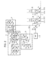
- a drive timing signal generator 5 according to the first embodiment is explained.
- the portions or elements corresponding to those in Fig. 1 are denoted by similar or same references.
- a pair of digit lines DL and DL are provided for each column and the data bus lines I/O1, I/O1 - 1/04, I/O4 and transfer gates QC1, QC'1 - QC4, QC'4 are provided in balanced manner to accord with the pairs of digit lines.
- a flip-flop type sense amplifier SA is provided to each pair of digit lines.
- the drive timing signal generator 5 is basically composed of a boot-strap circuit 11, a first capacitive pull-up circuit 12 and a second capacitive pull-up circuit 13.
- the boot-strap circuit 11 is composed of N-channel field effect transistors (N-MOSTs) Q 1 , to Q22 and a boot capacitor C., and generates an output signal of V cc through N-MOST Q 2 : in response to a precharge signal ⁇ p , and timing signals ⁇ , and ⁇ 2 which are generated in response to the chip enable signal CE .
- N-MOSTs N-channel field effect transistors
- the first capacitive pull-up circuit 12 is composed of N-MOSTs Q 23 to Q 26 and pull-up capacitors C.2 and C 3 , and further raises the V cc level output of the boot-strap circuit 11 above V cc thereby to generate the boosted level of YSE. in response to a timing signal ⁇ 3 generated in accordance with CE .
- the second boot circuit 13 is composed of N-MOSTs Q 30 to Q 33 and boost capacitors C 34 and C. s .
- the circuit 13 receives the precharge signal ⁇ p and a write timing signal o w which is generated in a write operation.
- the circuit 13 further boosts the level of YSE in the write operation in response to the rise of ow.
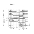
- the chip enable signal CE is changed to the low ("O") level at a time point t c to enable the memory for access. Then the precharge signal ⁇ P is fallen to the low level (ground level) at t.-. Then. the timing signal ⁇ . is raised to the high level at t to enable the circuit 11.
- the N-MOSTs Q 20 and Q 22 are turned off and the potential at N., is raised above V cc . Thus, the signals YSE and YjA are raised to V cc .
- the timing signal ⁇ 2 is then raised at a time point t 13 to V cc level to make N-MOST Q 18 conductive so that the level at node 14 is lowered and N-MOSTs Q,g to Q 22 are made non-conductive. As a result, the V cc level of YSE is maintained under high impedance, floating state.
- the timing signal ⁇ 3 is raised to V cc level so that nodes N. 6 and N., are raised above V cc through capacitors C 2 and C.,.
- the level of YSE is raised to V cc + VT (VT being a threshold voltage of N-MOSTs) or more, and the signal YjA is also raised to V cc + VT or more.
- transfer gate MOSTs QC,, QC', -QC 4 , QC' 4 are rendered conductive in the non-saturated, triode region thereby to provide large conductances between the four pairs of digit lines DL, DL and four pairs of bus lines I/O 1, I/O1 - I/O 4, I/O 4 so that read signals on the above digit lines are transferred to the data bus lines for outputting read information.
- the read/write control signal WE is changed to the low level and a write operation is initiated with respect to the same address on which the previous read operation has achieved.
- new data (low) signal is applied to the data bus line I/O 1 which has been at the high level. This change in potential at 1/0 1 is transmitted to the signal YSE through the stray capacitors C s to lower the level of YSE.
- the timing signal ⁇ w is activated to the high level at t17 so that the circuit 13 boosts the level of YSE above (V cc + VT) by the capacitive boost due to the capacitor C 4 and C 5 .
- the column decode signal YjA is again boosted to the level of (V cc + VT) or more so that the transfer gate N-MOSTs QC1, QC'1 - QC4, QC'4 are conducting in the non-saturated. triode region.
- the data bus lines 1,0 1. I.O 1 - I:O4, I/O 4 are connected to the four pairs of digit lines DL. DL via the large conductance of N-MOSTs QC1. QC'1 - QC4. QC'4 and the states of the sense amplifiers SA are easily inverted according to the new write data through the digit lines DL and DL which are set to D and V cc levels. respectively.
- CE is reset to the high level and the signals ⁇ - ⁇ 3 , and ⁇ w are all changed to the low level at t 20 .
- the precharge signal ⁇ p is raised and the digit lines DL, DL are precharged to terminate the operation.
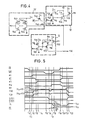
- a drive timing signal generator according to a second embodiment of the invention is featured by a CMOS buffer circuit 11' in place of the boot-strap circuit 11 in Fig. 2.
- the CMOS buffer circuit 11' is composed of P-channel MOSTs (P-MOSTs) Q41, Q43 and N-MOSTs Q42, Q44 to Q46.
- P-MOSTs P-channel MOSTs
- N-MOSTs N-MOSTs
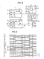
- a drive timing signal generator according to a third embodiment of the invention is featured by a write timing boot-strap circuit 14 and a coupling control circuit composed of N-MOSTs Q 63 -Q 55 . Also in place of 0 ⁇ w, three sequentially generated write timing signals 0 ⁇ W1 -0 ⁇ W3 are employed.
- the circuit 14 is composed of N-MOSTs Q 5 , to Q 62 and a capacitor C s . and has the similar circuit structure to the circuit 11.
- the circuit 14 produces the output of V cc level at a node N56 in response to the high level of 0 ⁇ W1 and renders the high level output at the high impedance, floating state.
- the high level of the output at the node N56 is transmitted to the outputs of the circuits 11, 12 and 13' via N-MOSFET Q 63 made conductive in response to 0 ⁇ W1 via O 64 . Then, when 0 ⁇ W3 goes to high in level, N-MOST Q 65 becomes conductive to make N-MOST Q 63 non-conductive so that the node N 56 is isolated from the outputs (YSE) of the circuits 11, 12 and 13'. While in response to the rise 0 ⁇ W3 , the circuit 13' capacitively boosts the level of YSE above (V cc + VT).
- Fig. 7 Operation of the circuit of Fig. 6 is illustrated in Fig. 7. As is apparent from Fig. 7, after WE goes to the low level at t. s . the timing signals 0 ⁇ W1 , 0 ⁇ W2 and 0 ⁇ W3 are sequentially produced at t 5 , t7 and t s respectively to boost YSE.
- Fig. 8 shows a a drive timing signal generator according to a fourth embodiment of the invention. This embodiment is obtained by adding a write timing CMOS buffer 14' and the coupling control circuit composed of N-MOSTs Q 65; -Q 55 ; to the embodiment of Fig. 4.
- the CMOS buffer 14' generates the V cc level at the node N56' in response to the high level of 0 wi and renders the high level at the node N56' at the high impedance, floating state in response to the low level of ⁇ W2 which is opposite to ⁇ w ⁇ .
- the present invention advantageously produces boosted level of drive timing signal for a long period, particularly for a write period subsequent to a read period.
Landscapes
- Dram (AREA)
- Static Random-Access Memory (AREA)
Applications Claiming Priority (4)
| Application Number | Priority Date | Filing Date | Title |
|---|---|---|---|
| JP19298/87 | 1987-01-28 | ||
| JP62019303A JPS63187493A (ja) | 1987-01-28 | 1987-01-28 | 信号発生回路 |
| JP62019298A JPS63184993A (ja) | 1987-01-28 | 1987-01-28 | 信号発生回路 |
| JP19303/87 | 1987-01-28 |
Publications (3)
| Publication Number | Publication Date |
|---|---|
| EP0276854A2 true EP0276854A2 (de) | 1988-08-03 |
| EP0276854A3 EP0276854A3 (de) | 1991-01-30 |
| EP0276854B1 EP0276854B1 (de) | 1993-10-20 |
Family
ID=26356130
Family Applications (1)
| Application Number | Title | Priority Date | Filing Date |
|---|---|---|---|
| EP88101243A Expired - Lifetime EP0276854B1 (de) | 1987-01-28 | 1988-01-28 | Halbleiterspeicheranordnung mit verbessertem Spalten-Auswahlschema |
Country Status (3)
| Country | Link |
|---|---|
| US (1) | US4878201A (de) |
| EP (1) | EP0276854B1 (de) |
| DE (1) | DE3884975T2 (de) |
Families Citing this family (10)
| Publication number | Priority date | Publication date | Assignee | Title |
|---|---|---|---|---|
| US5185721A (en) * | 1988-10-31 | 1993-02-09 | Texas Instruments Incorporated | Charge-retaining signal boosting circuit and method |
| US5751643A (en) * | 1990-04-06 | 1998-05-12 | Mosaid Technologies Incorporated | Dynamic memory word line driver |
| GB9007791D0 (en) * | 1990-04-06 | 1990-06-06 | Foss Richard C | High voltage boosted wordline supply charge pump and regulator for dram |
| GB2243233A (en) * | 1990-04-06 | 1991-10-23 | Mosaid Inc | DRAM word line driver |
| GB9007790D0 (en) * | 1990-04-06 | 1990-06-06 | Lines Valerie L | Dynamic memory wordline driver scheme |
| KR950009234B1 (ko) * | 1992-02-19 | 1995-08-18 | 삼성전자주식회사 | 반도체 메모리장치의 비트라인 분리클럭 발생장치 |
| US5604704A (en) * | 1994-05-30 | 1997-02-18 | Nec Corporation | Compound semiconductor static random access memory device equipped with precharging circuit controlled by boosted signal |
| US5581506A (en) * | 1994-06-03 | 1996-12-03 | Matsushita Electric Industrial Co., Ltd. | Level-shifter, semiconductor integrated circuit, and control methods thereof |
| KR100482737B1 (ko) * | 1997-12-11 | 2005-08-24 | 주식회사 하이닉스반도체 | 에스램의라이트드라이버회로 |
| US6487060B1 (en) * | 2001-05-30 | 2002-11-26 | Fujitsu Limited | Oxide protection for a booster circuit |
Family Cites Families (11)
| Publication number | Priority date | Publication date | Assignee | Title |
|---|---|---|---|---|
| US4239993A (en) * | 1978-09-22 | 1980-12-16 | Texas Instruments Incorporated | High performance dynamic sense amplifier with active loads |
| US4748349A (en) * | 1978-09-22 | 1988-05-31 | Texas Instruments Incorporated | High performance dynamic sense amplifier with voltage boost for row address lines |
| JPS5916195A (ja) * | 1982-07-19 | 1984-01-27 | Toshiba Corp | 半導体記憶装置 |
| DE3329874A1 (de) * | 1983-08-18 | 1985-03-07 | Siemens AG, 1000 Berlin und 8000 München | Mos-inverterschaltung |
| JPH07113863B2 (ja) * | 1985-06-29 | 1995-12-06 | 株式会社東芝 | 半導体集積回路装置 |
| JPS6252797A (ja) * | 1985-08-30 | 1987-03-07 | Mitsubishi Electric Corp | 半導体記憶装置 |
| US4750155A (en) * | 1985-09-19 | 1988-06-07 | Xilinx, Incorporated | 5-Transistor memory cell which can be reliably read and written |
| US4769784A (en) * | 1986-08-19 | 1988-09-06 | Advanced Micro Devices, Inc. | Capacitor-plate bias generator for CMOS DRAM memories |
| US4769792A (en) * | 1986-10-28 | 1988-09-06 | Kabushiki Kaisha Toshiba | Semiconductor memory device with voltage bootstrap |
| US4752699A (en) * | 1986-12-19 | 1988-06-21 | International Business Machines Corp. | On chip multiple voltage generation using a charge pump and plural feedback sense circuits |
| US4751679A (en) * | 1986-12-22 | 1988-06-14 | Motorola, Inc. | Gate stress test of a MOS memory |
-
1988
- 1988-01-28 US US07/149,269 patent/US4878201A/en not_active Expired - Lifetime
- 1988-01-28 DE DE88101243T patent/DE3884975T2/de not_active Expired - Fee Related
- 1988-01-28 EP EP88101243A patent/EP0276854B1/de not_active Expired - Lifetime
Also Published As
| Publication number | Publication date |
|---|---|
| US4878201A (en) | 1989-10-31 |
| EP0276854B1 (de) | 1993-10-20 |
| DE3884975D1 (de) | 1993-11-25 |
| DE3884975T2 (de) | 1994-02-10 |
| EP0276854A3 (de) | 1991-01-30 |
Similar Documents
| Publication | Publication Date | Title |
|---|---|---|
| US6351423B2 (en) | Semiconductor memory device including sense amplifier circuit differing in drivability between data write mode and data read mode | |
| US4301518A (en) | Differential sensing of single ended memory array | |
| KR0177776B1 (ko) | 고집적 반도체 메모리 장치의 데이타 센싱회로 | |
| US5619162A (en) | Dram using word line potential circuit control | |
| US4161040A (en) | Data-in amplifier for an MISFET memory device having a clamped output except during the write operation | |
| US5274598A (en) | Semiconductor memory having improved sensing arrangement | |
| JP3241280B2 (ja) | ダイナミック型半導体記憶装置 | |
| US4125878A (en) | Memory circuit | |
| US5091885A (en) | Dynamic type random-access memory having improved timing characteristics | |
| EP0069588A2 (de) | Integrierte Halbleiterspeicherschaltung | |
| US4606010A (en) | Dynamic memory device | |
| US4943952A (en) | Semiconductor memory circuit with improved bit lane precharge circuit | |
| EP0145488A2 (de) | Halbleiterspeicheranordnung | |
| US6728152B2 (en) | Sense amplifier for reduction of access device leakage | |
| US5650970A (en) | semiconductor memory device having a flash write function | |
| EP0316902A2 (de) | Halbleiterspeicherschaltung mit einem verbesserten Rückschreibschema | |
| US5323345A (en) | Semiconductor memory device having read/write circuitry | |
| US5818790A (en) | Method for driving word lines in semiconductor memory device | |
| US5014246A (en) | Semiconductor memory device having shared sense amplifier and operating method thereof | |
| US4878201A (en) | Semiconductor memory device having an improved timing signal generator for the column selection circuit | |
| US5148399A (en) | Sense amplifier circuitry selectively separable from bit lines for dynamic random access memory | |
| EP0373672B1 (de) | Halbleiterspeicherschaltung mit einer verbesserten Wiederherstellungssteuerschaltung | |
| US5668485A (en) | Row decoder with level translator | |
| JPH0146957B2 (de) | ||
| US4054865A (en) | Sense latch circuit for a bisectional memory array |
Legal Events
| Date | Code | Title | Description |
|---|---|---|---|
| PUAI | Public reference made under article 153(3) epc to a published international application that has entered the european phase |
Free format text: ORIGINAL CODE: 0009012 |
|
| 17P | Request for examination filed |
Effective date: 19880128 |
|
| AK | Designated contracting states |
Kind code of ref document: A2 Designated state(s): DE FR GB |
|
| PUAL | Search report despatched |
Free format text: ORIGINAL CODE: 0009013 |
|
| AK | Designated contracting states |
Kind code of ref document: A3 Designated state(s): DE FR GB |
|
| 17Q | First examination report despatched |
Effective date: 19920318 |
|
| GRAA | (expected) grant |
Free format text: ORIGINAL CODE: 0009210 |
|
| AK | Designated contracting states |
Kind code of ref document: B1 Designated state(s): DE FR GB |
|
| REF | Corresponds to: |
Ref document number: 3884975 Country of ref document: DE Date of ref document: 19931125 |
|
| ET | Fr: translation filed | ||
| PLBE | No opposition filed within time limit |
Free format text: ORIGINAL CODE: 0009261 |
|
| STAA | Information on the status of an ep patent application or granted ep patent |
Free format text: STATUS: NO OPPOSITION FILED WITHIN TIME LIMIT |
|
| 26N | No opposition filed | ||
| REG | Reference to a national code |
Ref country code: GB Ref legal event code: IF02 |
|
| PGFP | Annual fee paid to national office [announced via postgrant information from national office to epo] |
Ref country code: FR Payment date: 20020110 Year of fee payment: 15 |
|
| PGFP | Annual fee paid to national office [announced via postgrant information from national office to epo] |
Ref country code: GB Payment date: 20020130 Year of fee payment: 15 |
|
| PGFP | Annual fee paid to national office [announced via postgrant information from national office to epo] |
Ref country code: DE Payment date: 20020227 Year of fee payment: 15 |
|
| PG25 | Lapsed in a contracting state [announced via postgrant information from national office to epo] |
Ref country code: GB Free format text: LAPSE BECAUSE OF NON-PAYMENT OF DUE FEES Effective date: 20030128 |
|
| PG25 | Lapsed in a contracting state [announced via postgrant information from national office to epo] |
Ref country code: DE Free format text: LAPSE BECAUSE OF NON-PAYMENT OF DUE FEES Effective date: 20030801 |
|
| GBPC | Gb: european patent ceased through non-payment of renewal fee | ||
| PG25 | Lapsed in a contracting state [announced via postgrant information from national office to epo] |
Ref country code: FR Free format text: LAPSE BECAUSE OF NON-PAYMENT OF DUE FEES Effective date: 20030930 |
|
| REG | Reference to a national code |
Ref country code: FR Ref legal event code: ST |