EP0276897A2 - Verfahren zur Herstellung eines Trägers für optische Scheiben, wobei ein Träger mit einem Verteilungsgradienten der doppelten Refraktion ausgeglüht wird - Google Patents
Verfahren zur Herstellung eines Trägers für optische Scheiben, wobei ein Träger mit einem Verteilungsgradienten der doppelten Refraktion ausgeglüht wird Download PDFInfo
- Publication number
- EP0276897A2 EP0276897A2 EP88200156A EP88200156A EP0276897A2 EP 0276897 A2 EP0276897 A2 EP 0276897A2 EP 88200156 A EP88200156 A EP 88200156A EP 88200156 A EP88200156 A EP 88200156A EP 0276897 A2 EP0276897 A2 EP 0276897A2
- Authority
- EP
- European Patent Office
- Prior art keywords
- substrate
- double refraction
- optical disk
- forming
- annealing
- Prior art date
- Legal status (The legal status is an assumption and is not a legal conclusion. Google has not performed a legal analysis and makes no representation as to the accuracy of the status listed.)
- Granted
Links
- 239000000758 substrate Substances 0.000 title claims abstract description 54
- 230000003287 optical effect Effects 0.000 title claims abstract description 20
- 238000000034 method Methods 0.000 title claims abstract description 18
- 238000009826 distribution Methods 0.000 title claims abstract description 9
- 238000000137 annealing Methods 0.000 title claims description 6
- 229920000515 polycarbonate Polymers 0.000 claims abstract 2
- 239000004417 polycarbonate Substances 0.000 claims abstract 2
- 238000010438 heat treatment Methods 0.000 claims description 9
- 238000002347 injection Methods 0.000 claims description 4
- 239000007924 injection Substances 0.000 claims description 4
- 230000009477 glass transition Effects 0.000 claims description 3
- 238000001746 injection moulding Methods 0.000 claims description 3
- 239000004033 plastic Substances 0.000 description 7
- 239000010410 layer Substances 0.000 description 4
- 238000000465 moulding Methods 0.000 description 4
- 238000003860 storage Methods 0.000 description 3
- 230000015572 biosynthetic process Effects 0.000 description 2
- 229920005668 polycarbonate resin Polymers 0.000 description 2
- 239000004431 polycarbonate resin Substances 0.000 description 2
- 230000002035 prolonged effect Effects 0.000 description 2
- XAGFODPZIPBFFR-UHFFFAOYSA-N aluminium Chemical compound [Al] XAGFODPZIPBFFR-UHFFFAOYSA-N 0.000 description 1
- 229910052782 aluminium Inorganic materials 0.000 description 1
- 230000006835 compression Effects 0.000 description 1
- 238000007906 compression Methods 0.000 description 1
- 230000007423 decrease Effects 0.000 description 1
- 238000000151 deposition Methods 0.000 description 1
- 235000012489 doughnuts Nutrition 0.000 description 1
- 238000001035 drying Methods 0.000 description 1
- 238000005516 engineering process Methods 0.000 description 1
- 230000001747 exhibiting effect Effects 0.000 description 1
- 230000001678 irradiating effect Effects 0.000 description 1
- 238000004519 manufacturing process Methods 0.000 description 1
- 239000000463 material Substances 0.000 description 1
- 238000012986 modification Methods 0.000 description 1
- 230000004048 modification Effects 0.000 description 1
- 230000010287 polarization Effects 0.000 description 1
- 238000002360 preparation method Methods 0.000 description 1
- 239000011241 protective layer Substances 0.000 description 1
- 230000001105 regulatory effect Effects 0.000 description 1
- 238000009877 rendering Methods 0.000 description 1
Images


Classifications
-
- B—PERFORMING OPERATIONS; TRANSPORTING
- B29—WORKING OF PLASTICS; WORKING OF SUBSTANCES IN A PLASTIC STATE IN GENERAL
- B29C—SHAPING OR JOINING OF PLASTICS; SHAPING OF MATERIAL IN A PLASTIC STATE, NOT OTHERWISE PROVIDED FOR; AFTER-TREATMENT OF THE SHAPED PRODUCTS, e.g. REPAIRING
- B29C45/00—Injection moulding, i.e. forcing the required volume of moulding material through a nozzle into a closed mould; Apparatus therefor
- B29C45/17—Component parts, details or accessories; Auxiliary operations
- B29C45/26—Moulds
- B29C45/263—Moulds with mould wall parts provided with fine grooves or impressions, e.g. for record discs
-
- G—PHYSICS
- G11—INFORMATION STORAGE
- G11B—INFORMATION STORAGE BASED ON RELATIVE MOVEMENT BETWEEN RECORD CARRIER AND TRANSDUCER
- G11B7/00—Recording or reproducing by optical means, e.g. recording using a thermal beam of optical radiation by modifying optical properties or the physical structure, reproducing using an optical beam at lower power by sensing optical properties; Record carriers therefor
- G11B7/24—Record carriers characterised by shape, structure or physical properties, or by the selection of the material
- G11B7/241—Record carriers characterised by shape, structure or physical properties, or by the selection of the material characterised by the selection of the material
- G11B7/252—Record carriers characterised by shape, structure or physical properties, or by the selection of the material characterised by the selection of the material of layers other than recording layers
- G11B7/253—Record carriers characterised by shape, structure or physical properties, or by the selection of the material characterised by the selection of the material of layers other than recording layers of substrates
-
- G—PHYSICS
- G11—INFORMATION STORAGE
- G11B—INFORMATION STORAGE BASED ON RELATIVE MOVEMENT BETWEEN RECORD CARRIER AND TRANSDUCER
- G11B7/00—Recording or reproducing by optical means, e.g. recording using a thermal beam of optical radiation by modifying optical properties or the physical structure, reproducing using an optical beam at lower power by sensing optical properties; Record carriers therefor
- G11B7/24—Record carriers characterised by shape, structure or physical properties, or by the selection of the material
- G11B7/26—Apparatus or processes specially adapted for the manufacture of record carriers
- G11B7/263—Preparing and using a stamper, e.g. pressing or injection molding substrates
-
- B—PERFORMING OPERATIONS; TRANSPORTING
- B29—WORKING OF PLASTICS; WORKING OF SUBSTANCES IN A PLASTIC STATE IN GENERAL
- B29C—SHAPING OR JOINING OF PLASTICS; SHAPING OF MATERIAL IN A PLASTIC STATE, NOT OTHERWISE PROVIDED FOR; AFTER-TREATMENT OF THE SHAPED PRODUCTS, e.g. REPAIRING
- B29C45/00—Injection moulding, i.e. forcing the required volume of moulding material through a nozzle into a closed mould; Apparatus therefor
- B29C45/17—Component parts, details or accessories; Auxiliary operations
- B29C45/72—Heating or cooling
- B29C45/73—Heating or cooling of the mould
- B29C2045/7343—Heating or cooling of the mould heating or cooling different mould parts at different temperatures
Definitions
- the present invention relates to a process for producing a disk-shaped substrate adpated for use as substrate for compact disk, video disk, optical recording disk, magnetooptical recording disk or the like.
- an optical disk is prepared by forming, on a face of a substrate 1 of a disk form or doughnut form (in this text a disk form in which a central concentric portion is removed), a recording surface 2 on which information is recorded or which is capable of recording information.
- a recording surface 2 on which information is recorded or which is capable of recording information.
- said information recording surface 2 can be formed by forming a train of pits representing information on the surface of the substrate and depositing thereon a reflective film composed for example of aluminum.
- said information recording surface 2 can be formed by forming a recording layer, capable of optical information recording and reproduction, on the substrate. In this case spiral or concentric guide grooves are often formed on the surface of the substrate. Such recording surface 2 is usually formed in an annular area of a predetermined width on the substrate.
- the information recorded on an optical disk is read by irradiating the disk with a light beam from a side opposite to said recording surface, and converting the change in intensity of the light beam, which is transmitted in the substrate and reflected by the recording surface, into an electrical signal.
- an optical disk it is an important target to reduce the loss in said intensity change, since a large double refraction in the light-transmitting member will reduce the intensity of light emerging from the disk, thus rendering the signal reading more difficult. Consequently in the conventional process, the substrate for optical disk has been so prepared that the double refraction is substantially zero over the entire surface when the substrate is completed.
- the substrate prepared in this manner has been associated with a drawback, even if it is free from double refraction immediately after the preparation of showing considerable double refraction in the vicinity of the external periphery and in an area somewhat distant from said external periphery, as the result of exposure to high temperature in the formation of the reflective film thereon or in the transportation of the optical disk, or as the result of extended storage.
- the object of the present invention is to avoid the above-mentioned drawbacks in the prior technology and to provide a process for producing a substrate for optical disk, in which double refraction is reduced even after heating or prolonged storage.
- the above-mentioned object can be achieved, according to the present invention, by a process of producing a substrate for optical disk, comprising steps of molding a disk-shaped by means of polycarbonate resin with such a gradient distribution of double refraction that the value of said double refraction is in a range from -10 to -30 nm in the vicinity of external periphery and from +10 to +30 nm in the vicinity of center, and annealing thus molded substrate.
- the above-mentioned values of double refraction are usually defined in positions corresponding to the information recording area.
- the above-mentioned molding of substrate is made in such a manner that the double refraction is in a range from -10 to -30 nm at the external periphery of the information recording area and from +10 to +30 nm at the internal periphery of said area.
- the magnitude of the double refraction is measured by a polarization microscope and is considered positive or negative respectively in a compression stress state or a tension stress state in the radial direction of the substrate.
- Figs. 2A to 2C illustrate the process of producing an optical disk substrate according to the present invention.
- a substrate 1 is injection molded by means of molds 3, 4.
- the temperature of the molds is elevated to 110 - 130°C or selected higher by 10 - 20°C at the internal periphery than at the external periphery, in order that the substrate after molding has a double refraction in a range of -10 to -30 nm in the vicinity of the external periphery of the recording area and in a range of +10 to +30 nm in the vicinity of the internal periphery thereof.
- the injection speed may be gradually increased from the internal periphery toward the external periphery.
- the double refraction should remain almost constant on any concentric circle, and, more specifically, the fluctuation on a concentric circle should not exceed 5 nm.
- the substrate is taken out from the molds 3, 4 as shown in Fig. 2B, and is annealed by heating for example in a drying oven 5 as shown in Fig. 2C.
- the heating is preferably conducted at a temperature lower by 10 - 60°C than the glass transition temperature of the plastic substrate, for a period of 1 to 6 hours, but these conditions are suitably regulated according to the plastic material employed and the thickness of the substrate.
- the substrate after annealing shows reduced double refraction at the external and internal peripheries, thus exhibiting limited double refraction over the entire surface.
- An optical disk is prepared by forming a recording layer, a reflective layer, a protective layer etc. on thus molded substrate.
- This substrate scarcely shows increase in the double refraction even by heating at the formation of the recording layer etc. or even after prolonged storage.
- Fig. 3A shows the double refraction in a single pass (double refraction for the light transmitted once through the substrate) of said substrate immediately after molding, wherein the abscissa indicates the distance R from the center of disk, while the ordinate indicates the single-pass double refraction ⁇ n.
- the double refraction preferably decreases gradually from the internal periphery of the recording area toward the external periphery and falls rapidly to the negative range in the vicinity of the external periphery, as shown in Fig. 3A.
- Said plastic substrate was then annealed (6 hours in an oven of 90°C) to obtain an optical disk substrate.
- Fig. 3B shows the double refraction of said substrate after annealing.
- the range of double refraction which was as large as ⁇ 20 nm, could be reduced to ⁇ 10 nm by suitable heat treatment.
- Fig. 3C shows the double refraction of said substrate after it was again placed in an oven of 90°C for 6 hours. It is evident that the double refraction, after suitable heat treatment, no longer changes by repeated heat application.
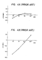
- a similar plastic substrate was prepared by injection molding in the same manner as in the foregoing example, except that the double refraction was maintained low over the entire surface according to the conventional process, as shown in Fig. 4A.
- Fig. 4B shows the double refraction obtained after said plastic substrate was subjected to heat treatment of 6 hours at 90°C.
- the substrated prepared in the conventional process shows an area of undesirably high double refraction after heating.
- the present invention is not limited to the foregoing embodiment but can be used in various applications. For example it is applicable in the production of optical disks in which information is detected by the light transmitted by the recording surface.
- the present invention includes such modifications and applications, as long as it is within the scope and spirit of the appended claims.
Landscapes
- Engineering & Computer Science (AREA)
- Manufacturing & Machinery (AREA)
- Mechanical Engineering (AREA)
- Manufacturing Optical Record Carriers (AREA)
- Injection Moulding Of Plastics Or The Like (AREA)
- Optical Record Carriers And Manufacture Thereof (AREA)
- Processing And Handling Of Plastics And Other Materials For Molding In General (AREA)
Applications Claiming Priority (2)
| Application Number | Priority Date | Filing Date | Title |
|---|---|---|---|
| JP18476/87 | 1987-01-30 | ||
| JP62018476A JPH0757499B2 (ja) | 1987-01-30 | 1987-01-30 | 光デイスク基板の製造法 |
Publications (3)
| Publication Number | Publication Date |
|---|---|
| EP0276897A2 true EP0276897A2 (de) | 1988-08-03 |
| EP0276897A3 EP0276897A3 (en) | 1990-08-22 |
| EP0276897B1 EP0276897B1 (de) | 1994-04-06 |
Family
ID=11972693
Family Applications (1)
| Application Number | Title | Priority Date | Filing Date |
|---|---|---|---|
| EP88200156A Expired - Lifetime EP0276897B1 (de) | 1987-01-30 | 1988-01-29 | Verfahren zur Herstellung eines Trägers für optische Scheiben, wobei ein Träger mit einem Verteilungsgradienten der doppelten Refraktion ausgeglüht wird |
Country Status (4)
| Country | Link |
|---|---|
| US (1) | US4892692A (de) |
| EP (1) | EP0276897B1 (de) |
| JP (1) | JPH0757499B2 (de) |
| DE (1) | DE3888857T2 (de) |
Cited By (1)
| Publication number | Priority date | Publication date | Assignee | Title |
|---|---|---|---|---|
| NL1005502C2 (nl) * | 1997-03-12 | 1998-09-15 | Ict Axxicon Bv | Matrijs voor het vervaardigen van schijfvormige voorwerpen. |
Families Citing this family (4)
| Publication number | Priority date | Publication date | Assignee | Title |
|---|---|---|---|---|
| JPH01160620A (ja) * | 1987-12-18 | 1989-06-23 | Sekisui Chem Co Ltd | 光ディスク基板の製造方法 |
| JP3032587B2 (ja) * | 1990-12-28 | 2000-04-17 | ティーディーケイ株式会社 | 光ディスクの製造方法 |
| US6007878A (en) * | 1993-05-27 | 1999-12-28 | Canon Kabushiki Kaisha | Process for producing an optical recording medium having a protective layer formed using a plasma processing device |
| CN1195313A (zh) * | 1996-05-10 | 1998-10-07 | 索尼株式会社 | 盘基板成形用金属模具及其制造方法以及盘基板 |
Family Cites Families (3)
| Publication number | Priority date | Publication date | Assignee | Title |
|---|---|---|---|---|
| JPS58126119A (ja) * | 1982-01-22 | 1983-07-27 | Mitsubishi Chem Ind Ltd | 光学的特性のすぐれた成形物の製造法 |
| JPS6067124A (ja) * | 1983-09-22 | 1985-04-17 | Daicel Chem Ind Ltd | 高密度情報記録担体用プラスチックディスクの射出成形用スタンパー |
| JPS60155424A (ja) * | 1984-01-26 | 1985-08-15 | Daicel Chem Ind Ltd | 大径のポリカ−ボネ−ト製光デイスク基板およびその製造法 |
-
1987
- 1987-01-30 JP JP62018476A patent/JPH0757499B2/ja not_active Expired - Lifetime
-
1988
- 1988-01-26 US US07/148,687 patent/US4892692A/en not_active Expired - Lifetime
- 1988-01-29 EP EP88200156A patent/EP0276897B1/de not_active Expired - Lifetime
- 1988-01-29 DE DE3888857T patent/DE3888857T2/de not_active Expired - Fee Related
Cited By (3)
| Publication number | Priority date | Publication date | Assignee | Title |
|---|---|---|---|---|
| NL1005502C2 (nl) * | 1997-03-12 | 1998-09-15 | Ict Axxicon Bv | Matrijs voor het vervaardigen van schijfvormige voorwerpen. |
| EP0864411A1 (de) * | 1997-03-12 | 1998-09-16 | Axxicon Moulds Eindhoven B.V. | Form zum Herstellen von scheibenförmigen Gegenständen |
| US6322350B1 (en) | 1997-03-12 | 2001-11-27 | Axxicon Moulds Eindhoven B.V. | Mould for manufacturing disc-like objects |
Also Published As
| Publication number | Publication date |
|---|---|
| DE3888857D1 (de) | 1994-05-11 |
| EP0276897A3 (en) | 1990-08-22 |
| DE3888857T2 (de) | 1994-08-04 |
| EP0276897B1 (de) | 1994-04-06 |
| JPH0757499B2 (ja) | 1995-06-21 |
| JPS63188013A (ja) | 1988-08-03 |
| US4892692A (en) | 1990-01-09 |
Similar Documents
| Publication | Publication Date | Title |
|---|---|---|
| US6246656B1 (en) | Reduced thickness of a light transmissive layer for a high density optical disc | |
| US6221455B1 (en) | Multi-layer optical disc and recording/reproducing apparatus | |
| KR19980080645A (ko) | 광학 기록 매체 및 광디스크 장치 | |
| US5615182A (en) | Magneto-optical disk and the reproducing method thereof | |
| EP0276897B1 (de) | Verfahren zur Herstellung eines Trägers für optische Scheiben, wobei ein Träger mit einem Verteilungsgradienten der doppelten Refraktion ausgeglüht wird | |
| US5180595A (en) | Metal mold for resin substrate for an optical recording medium | |
| US5694379A (en) | Magneto-optical recording medium and recording apparatus therefor | |
| US5883879A (en) | High density optical disc configuration | |
| US6269070B1 (en) | Optical disc having specified track pitch, push-pull signal, and cross-track signal | |
| JP2683520B2 (ja) | 光ディスク基板の製造法 | |
| JPS63220439A (ja) | 光磁気デイスクの製法 | |
| US4876133A (en) | Optical data recording system and method of production of recording medium | |
| JP2685092B2 (ja) | 光情報記録媒体及びその製造方法 | |
| KR100257889B1 (ko) | 광기록 매체 | |
| US7651752B2 (en) | Super resolution optical disc | |
| JPS5960747A (ja) | 磁気光学再生装置 | |
| JPS6265255A (ja) | 光磁気デイスク記録再生装置 | |
| KR100320474B1 (ko) | 고밀도 광디스크 제조 방법 및 재생 방법 | |
| JPH03130948A (ja) | 光情報記録媒体 | |
| JPS6314343A (ja) | 情報記録媒体 | |
| JPS6350936A (ja) | 光デイスク | |
| JP2001229575A (ja) | 光情報記録媒体 | |
| JP2003045083A (ja) | 光記録媒体及び光記録再生装置 | |
| JPS60184885A (ja) | 光学記録媒体 | |
| JPH0944910A (ja) | 光ディスクの製造方法 |
Legal Events
| Date | Code | Title | Description |
|---|---|---|---|
| PUAI | Public reference made under article 153(3) epc to a published international application that has entered the european phase |
Free format text: ORIGINAL CODE: 0009012 |
|
| AK | Designated contracting states |
Kind code of ref document: A2 Designated state(s): DE FR GB IT NL |
|
| PUAL | Search report despatched |
Free format text: ORIGINAL CODE: 0009013 |
|
| AK | Designated contracting states |
Kind code of ref document: A3 Designated state(s): DE FR GB IT NL |
|
| 17P | Request for examination filed |
Effective date: 19901228 |
|
| 17Q | First examination report despatched |
Effective date: 19920522 |
|
| GRAA | (expected) grant |
Free format text: ORIGINAL CODE: 0009210 |
|
| AK | Designated contracting states |
Kind code of ref document: B1 Designated state(s): DE FR GB IT NL |
|
| REF | Corresponds to: |
Ref document number: 3888857 Country of ref document: DE Date of ref document: 19940511 |
|
| ET | Fr: translation filed | ||
| ITF | It: translation for a ep patent filed | ||
| ITTA | It: last paid annual fee | ||
| PLBE | No opposition filed within time limit |
Free format text: ORIGINAL CODE: 0009261 |
|
| STAA | Information on the status of an ep patent application or granted ep patent |
Free format text: STATUS: NO OPPOSITION FILED WITHIN TIME LIMIT |
|
| 26N | No opposition filed | ||
| REG | Reference to a national code |
Ref country code: GB Ref legal event code: IF02 |
|
| PGFP | Annual fee paid to national office [announced via postgrant information from national office to epo] |
Ref country code: FR Payment date: 20060110 Year of fee payment: 19 |
|
| PGFP | Annual fee paid to national office [announced via postgrant information from national office to epo] |
Ref country code: NL Payment date: 20060115 Year of fee payment: 19 |
|
| PGFP | Annual fee paid to national office [announced via postgrant information from national office to epo] |
Ref country code: GB Payment date: 20060125 Year of fee payment: 19 |
|
| PGFP | Annual fee paid to national office [announced via postgrant information from national office to epo] |
Ref country code: DE Payment date: 20060126 Year of fee payment: 19 |
|
| PGFP | Annual fee paid to national office [announced via postgrant information from national office to epo] |
Ref country code: IT Payment date: 20060131 Year of fee payment: 19 |
|
| PG25 | Lapsed in a contracting state [announced via postgrant information from national office to epo] |
Ref country code: DE Free format text: LAPSE BECAUSE OF NON-PAYMENT OF DUE FEES Effective date: 20070801 |
|
| GBPC | Gb: european patent ceased through non-payment of renewal fee |
Effective date: 20070129 |
|
| NLV4 | Nl: lapsed or anulled due to non-payment of the annual fee |
Effective date: 20070801 |
|
| REG | Reference to a national code |
Ref country code: FR Ref legal event code: ST Effective date: 20070930 |
|
| PG25 | Lapsed in a contracting state [announced via postgrant information from national office to epo] |
Ref country code: GB Free format text: LAPSE BECAUSE OF NON-PAYMENT OF DUE FEES Effective date: 20070129 |
|
| PG25 | Lapsed in a contracting state [announced via postgrant information from national office to epo] |
Ref country code: NL Free format text: LAPSE BECAUSE OF NON-PAYMENT OF DUE FEES Effective date: 20070801 |
|
| PG25 | Lapsed in a contracting state [announced via postgrant information from national office to epo] |
Ref country code: FR Free format text: LAPSE BECAUSE OF NON-PAYMENT OF DUE FEES Effective date: 20070131 |
|
| PG25 | Lapsed in a contracting state [announced via postgrant information from national office to epo] |
Ref country code: IT Free format text: LAPSE BECAUSE OF NON-PAYMENT OF DUE FEES Effective date: 20070129 |