EP0279993A2 - Unterdrückungsschaltung von unerwünschten zeitlichen Abschnitten eines variablen Spannungssignals - Google Patents
Unterdrückungsschaltung von unerwünschten zeitlichen Abschnitten eines variablen Spannungssignals Download PDFInfo
- Publication number
- EP0279993A2 EP0279993A2 EP87311386A EP87311386A EP0279993A2 EP 0279993 A2 EP0279993 A2 EP 0279993A2 EP 87311386 A EP87311386 A EP 87311386A EP 87311386 A EP87311386 A EP 87311386A EP 0279993 A2 EP0279993 A2 EP 0279993A2
- Authority
- EP
- European Patent Office
- Prior art keywords
- input
- output
- operational amplifier
- signal
- circuit
- Prior art date
- Legal status (The legal status is an assumption and is not a legal conclusion. Google has not performed a legal analysis and makes no representation as to the accuracy of the status listed.)
- Granted
Links
Images


Classifications
-
- G—PHYSICS
- G11—INFORMATION STORAGE
- G11C—STATIC STORES
- G11C27/00—Electric analogue stores, e.g. for storing instantaneous values
- G11C27/02—Sample-and-hold arrangements
- G11C27/024—Sample-and-hold arrangements using a capacitive memory element
- G11C27/026—Sample-and-hold arrangements using a capacitive memory element associated with an amplifier
-
- H—ELECTRICITY
- H03—ELECTRONIC CIRCUITRY
- H03F—AMPLIFIERS
- H03F1/00—Details of amplifiers with only discharge tubes, only semiconductor devices or only unspecified devices as amplifying elements
- H03F1/30—Modifications of amplifiers to reduce influence of variations of temperature or supply voltage or other physical parameters
- H03F1/303—Modifications of amplifiers to reduce influence of variations of temperature or supply voltage or other physical parameters using a switching device
Definitions
- This invention relates to circuits for removing unwanted temporal portions of voltage varying signals and has particular application to deriving such signals for driving servo-mechanisms where the unprocessed signals contain undesirable portions.
- the present invention is particularly useful for signals in which a desired portion of a signal contains a leg of relatively mild slope and a rapid leg of relatively large opposite slope and has particular application to deriving useful velocity information from "tri-phase servo patterns".
- a circuit for removing unwanted temporal portions of a voltage varying signal on the occurrence of a reset signal and for differentiating a resultant corrected signal with respect to a reference voltage said circuit being characterised by: switch means responsive to said reset signal applied to a first input, said switch means, in operation, being responsive to said reset signal to divert a second input of the switch means to a second output from a first output and thence to return said second input to said first output; input capacitor means for receiving said input signal; first operational amplifier means having positive and negative inputs and an output connected to said second input of said switch means, the positive input being connected to receive a voltage representative of the current through said input capacitor means; storage capacitor means having one side connected to a reference voltage and having its other side in electrical connection to the negative input of the first operational amplifier means and said first output of the switch means; inverting amplifier means connected to receive said second output of the switch means; and second operational amplifier means for receiving said corrected signal from the inverting amplifier means and having a negative input which is connected through
- the negative input of said second operational amplifier means is also connected to a reference voltage through the first resistor and a filter capacitor which is connected between a second resistor and said first resistor, the negative input of said second operational amplifier means being in electrical connection through both said first and second resistors to said input capacitor means, to the output of said inverting amplifier means and to said positive input of said first operational amplifier means.
- the negative input of said second operational amplifier means is in electrical connection with its output via said feedback resistor and a compensating capacitor connected in parallel therewith.
- a third resistor may be connected between said second resistor and said input capacitor means, said input capacitor means being connected through said third resistor with said inverting amplifier means and with said positive input of the first operational amplifier means.
- Said reset signal may be generated from a tri-phase servo signal.
- Said reset signal preferably is generated from the same tri-phase servo signal which is used to generate said input signal.
- a storage resistor is connected in series between said storage capacitor means and said negative input of said first operational amplifier means.
- One side of the storage resistor may be connected to said first output of the switch means and said negative input of the first operational amplifier means and the other side is connected to said storage capacitor means.
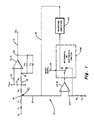
- FIG. 1 is a simplified diagram of a circuit 10 according to the present invention for removing unwanted temporal portions of a voltage varying signal.
- the term "line” used herein is to denote electrical connection via wire or other means.
- An input signal is provided to the circuit 10 at a point S1 charging a capacitor C1 and thence through resistors R1,R2,R3 to a negative input of an operational amplifier U1-A.
- the line between the resistor R3 and the negative input to the operational amplifier U1-A is also linked to a resistor R4 and a capacitor C3 which are connected in parallel between a point 21 and a point 22, on a line 14.
- the combination of the operational amplifier U1-A, the resistor R4 and the capacitor C3 constitutes a differentiator as shown in Figure 3.
- the line 14 is the output of the operational amplifier U1-A provided as output from the circuit 10 at a point S2.
- a positive input line 13 to the operational amplifier U1-A provides a reference voltage and is connected across a capacitor C2 to a point 12 on a signal input line 15. Between resistors R1,R2 on the signal input line, a point 16 connects a line 17 to the positive input of an operational amplifier U1-B.
- the line 17 is also connected to a line 18.
- the negative input of the operational amplifier U1-B is connected to ground (GND) through a resistor R5 and a capacitor C5 on a line 23.
- the output of the operational amplifier U1-B is selectively connected between: (a) a point on the line 23 between the negative input to the operational amplifier U1-B and the resistor R5, and (b) an approximate minus one or inverting amplifier U2.
- the selection is governed by a reset signal provided on a line 19 to a mechanical or electronic switch SW.
- the switch SW directs the output of the operational amplifier U1-B to the amplifier U2.
- the switch is set to provide the output of the operational amplifier U1-B to the line 23.
- the output of the amplifier U2 is provided on the line 18 to its connection to the line 17.
- the input signal charges the capacitor C1 and provides a voltage level V H at a point 16 which represents the charging current through the capacitor C1.
- V H the voltage level at a point 16 which represents the charging current through the capacitor C1.
- the operational amplifier U1-A connected as shown will tend to stabilise itself at a point where the voltage on the negative input is brought up to a voltage level V REF on the positive input. Therefore, the output voltage of the operational amplifier U1-A will tend to be proportional to the voltage level V H . It should be recognised that because the changes in the voltage level V H may be very small (about 0.1 millivolt) any ambient current leakage will affect the circuit performance This fact must be considered in component choice.
- the voltage level V H on the line 17 is provided as a positive input to the operational amplifier U1-B.
- the output of the operational amplifier U1-B is provided to the line 23 as input to the negative input of the operational amplifier U1-B and through the resistor R5 to the capacitor C5 and to ground, or as in a preferred embodiment, may employ a 5 volt reference in place of ground.
- the resistor R5 can provide filtering to the voltage provided to the capacitor C5 if desired.
- the switch SW transfers the output of the operational amplifier U1-B to the amplifier U2.
- the voltage level on the amplifier C5 provides an error voltage to the amplifier U2 which provides a voltage level equal to the voltage level on the capacitor C5 on the line 18 to the line 17 and to the point 16, thus sustaining the voltage level to the negative input of the operational amplifier U1-A during the reset interval.
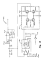
- FIG. 1A A more detailed schematic diagram of the circuit of Figure 1 is provided in Figure 1A in which the resistance and capacitance values are provided and reference made to standard industrial use numbers for designating particular integrated circuit and other component parts.
- the circuit is indicated by reference numeral 10A.
- Resistance, capacitance, and voltage values may be varied in accordance with known principles. Certain characteristics of some of the component parts shown, however, are important to prevent problems with ambient voltage affecting the performance of the differentiation characteristics of the operational amplifier U1-A.
- the amplifier U2 comprises a low leakage, high output impedance inverter amplifier when not operating so transistors Q3,Q4, for instance, must be low leakage transistors.
- the numbers 2N3906 and 2N3904 designates transistors of this type.
- Transistors Q1 and Q2 need not be low leakage transistors.
- the operational amplifier U1-B designated by the industry standard number LF412A (currently available through National Semiconductor Corporation) is a high speed operational amplifier with high input impedance (100 pico amp input), which will have no leakage current to affect the operation of the operational amplifier U1-A, which most likely will be on the same circuit board.
- Figure 4 illustrates a small segment of a possible non-ideal input signal 40.
- This signal will correspond to some portion of a signal WF1 whose waveform is shown in Figure 2. Because this signal is originally generated by digital circuits, it takes on a stairstep form as shown. Due probably primarily to irregularities on the data disk itself, transients or spikes t1,t2,t3 will often be found in the non-ideal input signal. These transients, as well as the stairstep configuration of the input signal 40, will be smoothed and filtered out by the circuit of Figure 1.
- the input signal 40 is indicated with reference to the voltage level V REF in Figure 4.
- reference voltage levels need not be the same DC potential for any of the three points to which they are introduced into the circuit but the potential values must be constant.
- a reference voltage level of 5 volts for the positive input of the operational amplifier was found to be best in practice to achieve the greatest dynamic range for the power supplies used.
- Figure 5 describes by a curve 41 a possible ideal output signal. Segment 42 corresponds to a negative output signal portion indicated by signal WF3 in Figure 2.
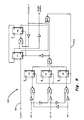
- FIG. 6 there is shown a circuit diagram of a circuit 100 through which the reset signal may be derived from tri-phase signals.
- Three triangle wave signals A,B,C are provided on lines 31,32,33, respectively.
- the triangle waves are derived from tri-phase spaced signals located in a formatted data disk used with the invention described in the aforementioned currently pending U.S. Patent Applications.
- the circuit 100 of Figure 6 provides an output signal from line 36 which forms the signal input at the point S1 of the circuit 10 of Figures 1 and 1A. A detailed representation of this output signal is found in Figure 8 and of the signals A,B,C is found at the top of Figure 7.
- a preferred decode circuit is explained with reference to Figure 9, which generates a reset signal during rapid transition periods in the servo position error signal, but other constructions to accomplish this are possible.
- the bit signals used to generate the reset signal are produced by the circuit 100 which acts in the following manner.
- the three phase signals A,B,C are compared by three comparators U81,U82,U83. Where the signal A on the line 31 is of higher voltage than the signal B on the line 32, the output of a non-inverting buffer circuit U21 is "high” and the output of an inverting circuit U11 is “low”. Otherwise, the reverse is the case.
- the two other comparators U82,U83 and their associated inverting circuits U12,U13 and non-inverting buffer circuits U22,U23 function in the same way for their inputs.
- the signals A,B,C are input into the circuit 100 on lines 31, 32 and 33 respectively.
- typical signals A, B and C are shown with respect to a reference voltage level V REF .
- the signals A,B,C are fed into the positive input of a respective one of the comparators U81,U82,U83.
- One of the other of the three signals A,B,C is input into the negative input of the comparators.
- "LM339" is the industry standard numerical designation for comparators used in a preferred embodiment and they are currently available from National Semiconductor Corporation.
- Each one of the signals A,B,C is also input to two of six analog switches U14 (1-6) to be passed through to inverting and non-inverting differential amplifier input lines 34,35, respectively, to create the servo position error signal SPE on line 36 as shown in Figures 7 and 8.
- the signals A, B and C input to the comparators U81,U82,U83 in turn drive the inverting circuits U11, U12,U13, and also drive the non-inverting buffer circuits U21,U22,U23.
- the output of these circuits provide the proper switching of the analog switches U14 (1-6) .
- Resistance/capacitor pairs 101,102,103 provide hysteresis to the respective comparators U81,U82,U83 to prevent multiple switching during noise transients which may appear in the signals A,B,C.
- a differential amplifier U19 produces a signal on the line 36 as shown in Figure 8.
- the alphanumeric indicators attached to the signal shown in Figure 8 correspond to the decimal or SPE indicators shown in Figure 7.
- bit signals of the comparators produced on the output lines B1,B2,B0 are shown in Figure 7 as 0, 1 and 2. Therefore, looking at the signals in a "head-in” direction in Figure 7, because the transition or unwanted signal portion occurs between areas designated 6 and 2, areas designated 3 and 1 and areas designated 5 and 4 (see Figure 5 and bottom of Figure 7) and because a downward going pulse occurs at each one of these area interfaces and because only one of the three bit signals is "high" at a downward going signal area, all that is necessary is to fire a reset signal at a downward going pulse. In a "head-out” direction each upward going pulse will signal that a reset signal is necessary; i.e., that the slope transition occurs at that interface.
- a microprocessor could receive these digital bit signals as input and based on a program generate a reset pulse at the proper upward or downward going transitions of each of the bit signals. It is simplest and most efficient to think of this in terms of the two EXCLUSIVE-OR gates 52,53 which will provide an output pulse of relatively short duration in conjunction with a digital one shot for each of the indicated transistors.
- a clock input which is a period length smaller than the desired duration of the reset signal, is provided to the circuit 200 at an input 201.
- the clock pulse should be a short portion of the clock period.
- the clock pulse (clock 1 in Figure 10) is provided as the clock input to a flip-flop F7.
- a second clock (clock 2 in Figure 10) provides a delayed clock to a NAND gate NA2, and its inverse is provided to a NOR gate N4.
- the Q output of the flip-flop F7 when "low” provides the reset signal used in the circuits 10 and 10A to control the switch SW.
- the circuit 200 receives the three bit signals from the circuit 100 of Figure 6 (shown in time relation to each other in Figure 7) as inputs. They are provided, inverted and non-inverted as input to NOR gates N1,N2,N3 respectively. The outputs of these NOR gates are input to respective flip-flops F4,F5,F6. The output of these flip-flops is input to NAND gate NA1 whose output is provided as an input to the NAND gate NA2. The output of the NAND gate NA1 clears the flip-flop F7. The NAND gate NA2 also receives the Q outputs of the flip-flops F7,F8 as inputs. The output of the NAND gate NA2 provides a clear signal to the flip-flops F4,F5,F6. The D inputs of the flip-flops F4,F5,F6,F8 are all tied to "high" signal or voltage level as indicated by arrows.
- circuit 200 of Figure 9 and its associated timing diagram of Figure 10 is only one possibility for providing efficient decode for the reset signal.
Landscapes
- Engineering & Computer Science (AREA)
- Power Engineering (AREA)
- Manipulation Of Pulses (AREA)
- Amplifiers (AREA)
- Moving Of Head For Track Selection And Changing (AREA)
- Moving Of The Head To Find And Align With The Track (AREA)
Priority Applications (1)
| Application Number | Priority Date | Filing Date | Title |
|---|---|---|---|
| EP91202141A EP0460775B1 (de) | 1987-02-27 | 1987-12-23 | Schaltung zur Erzeugung eines pulsförmigen Ausgangssignales aus drei binären Eingangssignalen |
Applications Claiming Priority (2)
| Application Number | Priority Date | Filing Date | Title |
|---|---|---|---|
| US07/020,289 US4760319A (en) | 1987-02-27 | 1987-02-27 | Circuit for removing unwanted slope transitions from an incoming signal |
| US20289 | 1987-02-27 |
Related Child Applications (1)
| Application Number | Title | Priority Date | Filing Date |
|---|---|---|---|
| EP91202141.7 Division-Into | 1987-12-23 |
Publications (3)
| Publication Number | Publication Date |
|---|---|
| EP0279993A2 true EP0279993A2 (de) | 1988-08-31 |
| EP0279993A3 EP0279993A3 (en) | 1989-07-05 |
| EP0279993B1 EP0279993B1 (de) | 1992-09-02 |
Family
ID=21797777
Family Applications (2)
| Application Number | Title | Priority Date | Filing Date |
|---|---|---|---|
| EP87311386A Expired EP0279993B1 (de) | 1987-02-27 | 1987-12-23 | Unterdrückungsschaltung von unerwünschten zeitlichen Abschnitten eines variablen Spannungssignals |
| EP91202141A Expired - Lifetime EP0460775B1 (de) | 1987-02-27 | 1987-12-23 | Schaltung zur Erzeugung eines pulsförmigen Ausgangssignales aus drei binären Eingangssignalen |
Family Applications After (1)
| Application Number | Title | Priority Date | Filing Date |
|---|---|---|---|
| EP91202141A Expired - Lifetime EP0460775B1 (de) | 1987-02-27 | 1987-12-23 | Schaltung zur Erzeugung eines pulsförmigen Ausgangssignales aus drei binären Eingangssignalen |
Country Status (6)
| Country | Link |
|---|---|
| US (1) | US4760319A (de) |
| EP (2) | EP0279993B1 (de) |
| JP (1) | JPS63217709A (de) |
| AU (1) | AU1004388A (de) |
| CA (1) | CA1336725C (de) |
| DE (2) | DE3751438T2 (de) |
Cited By (1)
| Publication number | Priority date | Publication date | Assignee | Title |
|---|---|---|---|---|
| FR2657719A1 (fr) * | 1990-01-30 | 1991-08-02 | Thomson Composants Militaires | Circuit d'echantillonnage de signaux analogiques. |
Families Citing this family (3)
| Publication number | Priority date | Publication date | Assignee | Title |
|---|---|---|---|---|
| JPH03188709A (ja) * | 1989-12-19 | 1991-08-16 | Hitachi Ltd | のこぎり波発生回路 |
| DE69411217T2 (de) * | 1993-04-05 | 1999-02-04 | Philips Electronics N.V., Eindhoven | Verzögerungsschaltung zum Verzögern von differentiellen Signalen |
| US9151827B2 (en) * | 2012-12-11 | 2015-10-06 | Infineon Technologies Ag | Compensating slowly varying if DC offsets in receivers |
Family Cites Families (19)
| Publication number | Priority date | Publication date | Assignee | Title |
|---|---|---|---|---|
| US3708737A (en) * | 1971-05-19 | 1973-01-02 | California Data Corp | Electric motor speed sensing |
| US3863080A (en) * | 1973-10-18 | 1975-01-28 | Rca Corp | Current output frequency and phase comparator |
| US4130786A (en) * | 1976-11-17 | 1978-12-19 | Xerox Corporation | Apparatus for generating linear and continuous positional error and velocity signals for higher order servo systems |
| JPS54119215A (en) * | 1978-03-09 | 1979-09-17 | Toshiba Corp | Magnetic disc apparatus |
| US4316155A (en) * | 1979-09-05 | 1982-02-16 | The Bendix Corporation | Voltage controlled oscillator having ratiometric and temperature compensation |
| US4321517A (en) * | 1979-12-03 | 1982-03-23 | Storage Technology Corporation | Resonance suppression method |
| US4300081A (en) * | 1980-03-14 | 1981-11-10 | General Motors Corporation | Motor voltage feedback for a servo motor control system |
| US4366422A (en) * | 1980-08-25 | 1982-12-28 | Rockwell International Corporation | Velocity sensing pulse pair servo apparatus |
| JPS5743205A (en) * | 1980-08-27 | 1982-03-11 | Hitachi Ltd | Speed feedback circuit |
| US4553052A (en) * | 1982-04-23 | 1985-11-12 | Nec Corporation | High speed comparator circuit with input-offset compensation function |
| ATE39588T1 (de) * | 1982-05-10 | 1989-01-15 | Digital Equipment Corp | Positioniersteuerungssystem mit sowohl kontinuierlichen als auch eingefuegten servoinformationen fuer einen magnetplattenspeicher. |
| EP0176596B1 (de) * | 1982-11-26 | 1990-07-18 | Mitsubishi Denki Kabushiki Kaisha | Analog-eingangsschaltung |
| US4480217A (en) * | 1982-12-14 | 1984-10-30 | Storage Technology Corporation | Automatic velocity calibrator for a velocity servo loop in a magnetic disk drive |
| US4514672A (en) * | 1983-04-06 | 1985-04-30 | Ampex Corporation | Adaptive apparatus and method for control |
| US4574813A (en) * | 1983-11-14 | 1986-03-11 | Hewlett-Packard Company | Pace pulse signal conditioning circuit |
| US4584559A (en) * | 1984-06-13 | 1986-04-22 | Tektronix, Inc. | Dual rank sample and hold circuit and method |
| GB2160731B (en) * | 1984-06-22 | 1987-09-03 | Ferranti Plc | Demodulator circuit |
| JPH0749524Y2 (ja) * | 1984-12-17 | 1995-11-13 | ナカミチ株式会社 | 移動体の移動制御装置 |
| US4701815A (en) * | 1985-03-11 | 1987-10-20 | Sony Corporation | Tracking servo system for disc memory |
-
1987
- 1987-02-27 US US07/020,289 patent/US4760319A/en not_active Expired - Lifetime
- 1987-10-21 JP JP62264064A patent/JPS63217709A/ja active Granted
- 1987-12-23 DE DE3751438T patent/DE3751438T2/de not_active Expired - Fee Related
- 1987-12-23 DE DE8787311386T patent/DE3781543T2/de not_active Expired - Fee Related
- 1987-12-23 EP EP87311386A patent/EP0279993B1/de not_active Expired
- 1987-12-23 EP EP91202141A patent/EP0460775B1/de not_active Expired - Lifetime
-
1988
- 1988-01-05 AU AU10043/88A patent/AU1004388A/en not_active Abandoned
- 1988-02-26 CA CA000559935A patent/CA1336725C/en not_active Expired - Fee Related
Cited By (3)
| Publication number | Priority date | Publication date | Assignee | Title |
|---|---|---|---|---|
| FR2657719A1 (fr) * | 1990-01-30 | 1991-08-02 | Thomson Composants Militaires | Circuit d'echantillonnage de signaux analogiques. |
| WO1991011812A3 (fr) * | 1990-01-30 | 1991-10-03 | Thomson Composants Militaires | Circuit d'echantillonnage de signaux analogiques |
| US5506525A (en) * | 1990-01-30 | 1996-04-09 | Thomson Composants Militaires Et Spatiaux | Sampling circuit for analog signals |
Also Published As
| Publication number | Publication date |
|---|---|
| DE3751438D1 (de) | 1995-09-07 |
| DE3781543D1 (de) | 1992-10-08 |
| DE3781543T2 (de) | 1993-05-27 |
| EP0460775A2 (de) | 1991-12-11 |
| AU1004388A (en) | 1988-09-01 |
| EP0279993A3 (en) | 1989-07-05 |
| EP0460775B1 (de) | 1995-08-02 |
| EP0279993B1 (de) | 1992-09-02 |
| JPH0432471B2 (de) | 1992-05-29 |
| JPS63217709A (ja) | 1988-09-09 |
| CA1336725C (en) | 1995-08-15 |
| DE3751438T2 (de) | 1996-01-04 |
| US4760319A (en) | 1988-07-26 |
| EP0460775A3 (en) | 1992-01-15 |
Similar Documents
| Publication | Publication Date | Title |
|---|---|---|
| KR920003447B1 (ko) | 슈미트트리거회로 | |
| US4773096A (en) | Digital switching power amplifier | |
| KR19990044515A (ko) | 고이득 모드와 저이득 모드를 갖는 펄스폭 변조디지털-아날로그 변환기 | |
| US5055708A (en) | Circuit for driving an inductive load | |
| EP0279993B1 (de) | Unterdrückungsschaltung von unerwünschten zeitlichen Abschnitten eines variablen Spannungssignals | |
| US6134252A (en) | Enhanced glitch removal circuit | |
| KR100373466B1 (ko) | D/a변환기 | |
| US5323065A (en) | Semiconductor integrated circuit device having edge trigger flip-flop circuit for decreasing delay time | |
| JP2006517768A (ja) | 電流dacのコード独立型スイッチ | |
| EP0598374A2 (de) | Abtastfrequenzumsetzer | |
| US6381086B1 (en) | Programmable active damping for high-speed write driver | |
| US4808998A (en) | Distortion reduction circuit for a D/A converter | |
| EP0156305B1 (de) | Digital/Analog-Wandler | |
| US5204982A (en) | Method and apparatus for digital switching of fm signals with reduced crosstalk | |
| US5604459A (en) | Method and apparatus for multiplying a pulse modulated signal by an analog control signal | |
| US4473819A (en) | Digital-to-analog conversion apparatus with a variable active-level | |
| JPS61152128A (ja) | デジタル・アナログ変換回路 | |
| JP3116706B2 (ja) | トリガ入力回路 | |
| US5025173A (en) | EFM-signal comparator | |
| JPS61256825A (ja) | Pwm型d/a変換装置 | |
| SU1324068A1 (ru) | Устройство дл контрол посто нной пам ти | |
| JPS6159016B2 (de) | ||
| KR960009035Y1 (ko) | 모터의 베이스 구동 제어회로 | |
| GB2071448A (en) | A Circuit for Processing an Information Signal | |
| EP0281009A2 (de) | Signal-Verarbeitungsschaltung |
Legal Events
| Date | Code | Title | Description |
|---|---|---|---|
| PUAI | Public reference made under article 153(3) epc to a published international application that has entered the european phase |
Free format text: ORIGINAL CODE: 0009012 |
|
| AK | Designated contracting states |
Kind code of ref document: A2 Designated state(s): DE FR GB |
|
| PUAL | Search report despatched |
Free format text: ORIGINAL CODE: 0009013 |
|
| AK | Designated contracting states |
Kind code of ref document: A3 Designated state(s): DE FR GB |
|
| 17P | Request for examination filed |
Effective date: 19891207 |
|
| RAP1 | Party data changed (applicant data changed or rights of an application transferred) |
Owner name: SEAGATE TECHNOLOGY INTERNATIONAL |
|
| 17Q | First examination report despatched |
Effective date: 19910214 |
|
| GRAA | (expected) grant |
Free format text: ORIGINAL CODE: 0009210 |
|
| AK | Designated contracting states |
Kind code of ref document: B1 Designated state(s): DE FR GB |
|
| XX | Miscellaneous (additional remarks) |
Free format text: TEILANMELDUNG 91202141.7 EINGEREICHT AM 23/12/87. |
|
| REF | Corresponds to: |
Ref document number: 3781543 Country of ref document: DE Date of ref document: 19921008 |
|
| ET | Fr: translation filed | ||
| PLBE | No opposition filed within time limit |
Free format text: ORIGINAL CODE: 0009261 |
|
| STAA | Information on the status of an ep patent application or granted ep patent |
Free format text: STATUS: NO OPPOSITION FILED WITHIN TIME LIMIT |
|
| 26N | No opposition filed | ||
| PGFP | Annual fee paid to national office [announced via postgrant information from national office to epo] |
Ref country code: FR Payment date: 19961125 Year of fee payment: 10 |
|
| PGFP | Annual fee paid to national office [announced via postgrant information from national office to epo] |
Ref country code: GB Payment date: 19971124 Year of fee payment: 11 Ref country code: DE Payment date: 19971124 Year of fee payment: 11 |
|
| PG25 | Lapsed in a contracting state [announced via postgrant information from national office to epo] |
Ref country code: FR Free format text: THE PATENT HAS BEEN ANNULLED BY A DECISION OF A NATIONAL AUTHORITY Effective date: 19971231 |
|
| REG | Reference to a national code |
Ref country code: FR Ref legal event code: ST |
|
| PG25 | Lapsed in a contracting state [announced via postgrant information from national office to epo] |
Ref country code: GB Free format text: LAPSE BECAUSE OF NON-PAYMENT OF DUE FEES Effective date: 19981223 |
|
| GBPC | Gb: european patent ceased through non-payment of renewal fee |
Effective date: 19981223 |
|
| PG25 | Lapsed in a contracting state [announced via postgrant information from national office to epo] |
Ref country code: DE Free format text: LAPSE BECAUSE OF NON-PAYMENT OF DUE FEES Effective date: 19991001 |