EP0281652B1 - Procédé d'obtention d'un signal de différence de phase - Google Patents
Procédé d'obtention d'un signal de différence de phase Download PDFInfo
- Publication number
- EP0281652B1 EP0281652B1 EP87103453A EP87103453A EP0281652B1 EP 0281652 B1 EP0281652 B1 EP 0281652B1 EP 87103453 A EP87103453 A EP 87103453A EP 87103453 A EP87103453 A EP 87103453A EP 0281652 B1 EP0281652 B1 EP 0281652B1
- Authority
- EP
- European Patent Office
- Prior art keywords
- signal
- amplitude
- phase angle
- phase
- signal components
- Prior art date
- Legal status (The legal status is an assumption and is not a legal conclusion. Google has not performed a legal analysis and makes no representation as to the accuracy of the status listed.)
- Expired - Lifetime
Links
- 238000000034 method Methods 0.000 title claims description 33
- 230000006870 function Effects 0.000 claims description 31
- 230000010363 phase shift Effects 0.000 claims description 7
- 239000013598 vector Substances 0.000 claims description 7
- 238000011084 recovery Methods 0.000 claims description 4
- 230000001419 dependent effect Effects 0.000 claims description 2
- 238000010586 diagram Methods 0.000 description 13
- 230000005540 biological transmission Effects 0.000 description 5
- 241001136792 Alle Species 0.000 description 2
- 238000013139 quantization Methods 0.000 description 2
- 230000008929 regeneration Effects 0.000 description 2
- 238000011069 regeneration method Methods 0.000 description 2
- 230000015572 biosynthetic process Effects 0.000 description 1
- 238000006243 chemical reaction Methods 0.000 description 1
- 230000004048 modification Effects 0.000 description 1
- 238000012986 modification Methods 0.000 description 1
- 238000005070 sampling Methods 0.000 description 1
- 230000009131 signaling function Effects 0.000 description 1
- 210000002023 somite Anatomy 0.000 description 1
- 230000001360 synchronised effect Effects 0.000 description 1
Images


Classifications
-
- H—ELECTRICITY
- H04—ELECTRIC COMMUNICATION TECHNIQUE
- H04L—TRANSMISSION OF DIGITAL INFORMATION, e.g. TELEGRAPHIC COMMUNICATION
- H04L27/00—Modulated-carrier systems
- H04L27/18—Phase-modulated carrier systems, i.e. using phase-shift keying
- H04L27/22—Demodulator circuits; Receiver circuits
- H04L27/227—Demodulator circuits; Receiver circuits using coherent demodulation
- H04L27/2271—Demodulator circuits; Receiver circuits using coherent demodulation wherein the carrier recovery circuit uses only the demodulated signals
- H04L27/2273—Demodulator circuits; Receiver circuits using coherent demodulation wherein the carrier recovery circuit uses only the demodulated signals associated with quadrature demodulation, e.g. Costas loop
-
- H—ELECTRICITY
- H04—ELECTRIC COMMUNICATION TECHNIQUE
- H04L—TRANSMISSION OF DIGITAL INFORMATION, e.g. TELEGRAPHIC COMMUNICATION
- H04L27/00—Modulated-carrier systems
- H04L27/32—Carrier systems characterised by combinations of two or more of the types covered by groups H04L27/02, H04L27/10, H04L27/18 or H04L27/26
- H04L27/34—Amplitude- and phase-modulated carrier systems, e.g. quadrature-amplitude modulated carrier systems
- H04L27/38—Demodulator circuits; Receiver circuits
-
- H—ELECTRICITY
- H04—ELECTRIC COMMUNICATION TECHNIQUE
- H04L—TRANSMISSION OF DIGITAL INFORMATION, e.g. TELEGRAPHIC COMMUNICATION
- H04L27/00—Modulated-carrier systems
- H04L27/0014—Carrier regulation
- H04L2027/0044—Control loops for carrier regulation
- H04L2027/0046—Open loops
-
- H—ELECTRICITY
- H04—ELECTRIC COMMUNICATION TECHNIQUE
- H04L—TRANSMISSION OF DIGITAL INFORMATION, e.g. TELEGRAPHIC COMMUNICATION
- H04L27/00—Modulated-carrier systems
- H04L27/0014—Carrier regulation
- H04L2027/0044—Control loops for carrier regulation
- H04L2027/0063—Elements of loops
- H04L2027/0067—Phase error detectors
Definitions
- the present invention relates to a method for obtaining a signal which reproduces the phase difference between a local carrier signal and the carrier of an amplitude-and / or phase-shift-keyed received signal, the method steps specified in the preamble of claim 1 being carried out.
- the invention has for its object to provide a method of the type mentioned above, with which a signal can be obtained which, even in the case of an amplitude disturbance or inaccurate amplitude setting of an OASK received signal, clearly informs when the phase difference between a local carrier signal and the OASK signal -Carrier is exactly 0 ° or an equivalent phase (e.g. with m-QAM 0 ° + n ⁇ 90 °, n gaz number).
- the method of the invention has the advantage that it can be implemented with relatively little circuitry and that even when applied to extremely high-level (e.g. 256-QAM) signals with amplitude and / or phase shift keying, the correct phase difference is very reliably obtained.
- extremely high-level e.g. 256-QAM
- QASK signals Telecommunication methods for information transmission by means of amplitude and / or phase shift keyed signals, also abbreviated to QASK signals, have become increasingly important in recent years.
- QASK signals can be described as follows:
- the m-stage quadrature amplitude modulation (QAM) method is of particular importance.
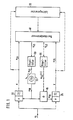
- FIG. 1 represents the known circuit principle of a quadrature receiver, which is suitable for demodulating QASK signals.
- a voltage-controlled oscillator (VCO) 10 has the task of a signal which is in phase-locked relation to the carrier of the input signal u1 (t): to create.
- the phase ⁇ depends on the VCO control signal originating from a control filter 50.
- a phase shifter 15 forms the signal u 10 (t) which is shifted by 90 °
- the downmixers 20 and 25 generate the signals from the input signal u 1 (t) and the signals u 10 (t) and u 15 (t) and
- the information about the clock frequency 1 / T and its phase position contained in U20 (t) and u 25 (t) can be used in a clock regenerator 30 in order to regenerate a clock signal in the correct phase.
- An example of a clock regenerator is based on an article by Le-Ngoc, Tho; Feher, Kamilo: A Digital Approach to Symbol Timing Recovery Systems in IEEE Trans. Com., Vol. COM-28, no.12, Dec. 1980, pp. 1993-1999.
- the output signal u 41 (t) of the baseband processor 40 described in detail below which is a function of the phase difference between the carrier of the received input signal u 1 (t) and the local carrier signal u 10 (t) generated in voltage controlled oscillator 10, is in the circuit 1 filtered in a control filter 50. Its output signal u s o (t) is the control signal for the voltage-controlled oscillator (VCO) 10.
- VCO voltage-controlled oscillator
- the down mixers 20, 25, the baseband processor 40, the control filter 50, the VCO 10 and the phase shifter 15 according to FIG. 1 form the control loop for local regeneration of the carrier of the input signal u 1 (t).
- blocks 20, 25, 10 and 15 form the quadrature receiver.
- the phase shifter 15 in the circuit according to FIG. 1 can be constructed such that a fine adjustment of the phase shift is possible via a control signal.
- the acquisition of the additional control information u 4 2 (t) required for this can also be obtained in the baseband processor 40.
- control signal U42 (t) which is a function of the phase difference 8 between the carrier signal components u io (t) and u 15 (t) and is determined in a similar manner to the signal u 41 (t) , connected to a control filter 55, the output signal u 55 (t) is fed to the control input of the phase shifter 15.
- the downmixers 20, 25, the baseband processor 40, the control filter 55, the local oscillator 10 and the phase shifter 15 form the control loop for tracking the phase difference 8 to the value 0 ° .
- the baseband processor is to be described, with which a signal dependent on the phase difference between the local carrier signal and the carrier of the received signal can be formed, which signal only becomes zero when the phase difference is actually 0 ° or ien equivalent phase.
- the normal and quadrature components x and y complex envelope of the received signal u i (t) are formed in the quadrature receiver of FIG. 1.
- the quadrature receiver thus generates two Cartesian-oriented signal components x and y.
- Cartesian-oriented signal components x and y are now converted into two polar-oriented signal components transformed, wherein the polar signal component R represents the amplitude of a signal state vector formed by the two Cartesian-oriented signal components x and y and the other polar signal component a represents the phase angle to this signal state vector.
- the correct amplitude of the transmitted signal state (a K , b K ) can also be determined from R the amplitude of a received signal state if its signal components x and y are slightly falsified by noise or by shifting the sampling time compared to kT.
- the threshold value decider for the amplitude must then be able to generate precisely these r output values.
- the possible nominal amplitudes are contained in the range of values ⁇ 1,414, 3,162, 4,234, 5,099, 5,831, 7,071, 7,616, 8,602, 9,899.
- the amplitude thresholds are formed as the arithmetic mean of adjacent nominal amplitudes, then the amplitude R of the received signal is decided to R e -7.071.
- the range of phase angle values belongs to the nominal amplitude R 6
- the phase difference between the actual value and the setpoint value, which serves as the control variable for the voltage-controlled oscillator, is then 14.45 ° .
- the rule sign is positive in this particular example.
- the amplitude is only determined relatively imprecisely due to imperfections in the amplitude control.
- the signal state (5.5) is sent.
- the received amplitude is about 6.4% too large.
- a lower limit value R m i n arises by subtracting an amount d 1 from the amplitude R
- the upper limit value Rmax arises by adding an amount d 2 to the amplitude R.
- the amounts d i and d 2 can be chosen to be large enough to apply 0 ⁇ d 1 ⁇ R and d 2 > 0.
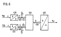
- FIG. 3 shows a block diagram for determining a phase difference signal according to the method described above.
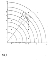
- Fig. 1 shows a section of a signal state diagram e.g. of a 64 QAM system.
- the dots indicate the possible signal states with an ideally regenerated carrier.
- Each of these points lies in a so-called decision area, which is delimited on the one hand by the thresholds of the amplitude value decision drawn as circles and on the other hand by the thresholds (not shown in FIG. 2) of the phase angle decision.
- ⁇ 1 ⁇
- w (R m, Rmax, ⁇ ) is only - w mentioned below - a non-negative function of the position of the limit values Rmin and Rmax, and the phase angle a.
- w is called the weighting function. With w it is possible to emphasize some phase detector functions over others.
- the signal state diagram in Fig. 2 reveals that there are some amplitude ranges in which angular misjudgment is less likely than in others. These are the amplitude ranges in which there are only a few signal states.
- phase detector function ⁇ 1 ( ⁇ ) ⁇ - ⁇
- one of the phase detector functions E2 ( ⁇ ) according to equation (18) or ⁇ 4 ( ⁇ ) according to equation (20) is also to be realized with the circuit shown in FIG the output of the summer 416 is switched to a hard limiter 418 to form the signal function sgn ( ⁇ - ⁇ ).
- the switching block 418 is replaced by a short circuit.
- phase detector function ⁇ 6 ( ⁇ ) w (R m in, Rmax, a) sgn (a -) derived decision diagram for a 64QAM signal is shown in FIG. 4 and only its 1st quadrant, because in the 2nd or 3rd or fourth quadrant, the decision - making areas by rotation by 90 °, 180 ° and 270 ° emerge from the decision area of the first quadrant.
- phase detector function e 5 ( ⁇ ) or es ( ⁇ ), hereinafter referred to briefly as ⁇ ( ⁇ ), can be determined using a particularly simple method.
- phase detector characteristic which is defined by the memory content, can easily be changed by exchanging the memory or its content.
Landscapes
- Engineering & Computer Science (AREA)
- Computer Networks & Wireless Communication (AREA)
- Signal Processing (AREA)
- Digital Transmission Methods That Use Modulated Carrier Waves (AREA)
Claims (8)


du signal, définies en coordonnées cartésiennes, qui forme respectivement l'un des états quantifiés possibles du signal, en deux composantes du signal définies en coordonnées polaires, dont la première composante polaire du signal représente l'amplitude d'un vecteur d'état du signal formé par les deux composantes quantifiées, définies en coordonnées polaires,


du signal et dont l'autre composante polaire du signal représente l'angle de phase
correspondant à ce vecteur d'état du signal.
Priority Applications (4)
| Application Number | Priority Date | Filing Date | Title |
|---|---|---|---|
| DE8787103453T DE3766614D1 (de) | 1987-03-10 | 1987-03-10 | Verfahren zum gewinnen eines phasendifferenzsignals. |
| EP87103453A EP0281652B1 (fr) | 1987-03-10 | 1987-03-10 | Procédé d'obtention d'un signal de différence de phase |
| CA000560772A CA1285618C (fr) | 1987-03-10 | 1988-03-08 | Methode pour obtenir un signal de difference de phase |
| US07/165,715 US4843616A (en) | 1987-03-10 | 1988-03-08 | Method of obtaining a phase difference signal |
Applications Claiming Priority (1)
| Application Number | Priority Date | Filing Date | Title |
|---|---|---|---|
| EP87103453A EP0281652B1 (fr) | 1987-03-10 | 1987-03-10 | Procédé d'obtention d'un signal de différence de phase |
Publications (2)
| Publication Number | Publication Date |
|---|---|
| EP0281652A1 EP0281652A1 (fr) | 1988-09-14 |
| EP0281652B1 true EP0281652B1 (fr) | 1990-12-05 |
Family
ID=8196820
Family Applications (1)
| Application Number | Title | Priority Date | Filing Date |
|---|---|---|---|
| EP87103453A Expired - Lifetime EP0281652B1 (fr) | 1987-03-10 | 1987-03-10 | Procédé d'obtention d'un signal de différence de phase |
Country Status (4)
| Country | Link |
|---|---|
| US (1) | US4843616A (fr) |
| EP (1) | EP0281652B1 (fr) |
| CA (1) | CA1285618C (fr) |
| DE (1) | DE3766614D1 (fr) |
Cited By (1)
| Publication number | Priority date | Publication date | Assignee | Title |
|---|---|---|---|---|
| US8774323B2 (en) | 2006-12-29 | 2014-07-08 | Entropic Communications, Inc. | Device and method for determining a symbol during reception of a signal coupled with a quadrature signal pair (I,Q) for QAM frequency control and/or rotation control |
Families Citing this family (14)
| Publication number | Priority date | Publication date | Assignee | Title |
|---|---|---|---|---|
| EP0378719B1 (fr) * | 1989-01-18 | 1994-04-27 | Siemens Aktiengesellschaft | Générateur de distorsions numérique |
| US5058136A (en) * | 1990-12-17 | 1991-10-15 | Motorola, Inc. | Coherent detection for QPSK modulation |
| US5495497A (en) * | 1991-09-25 | 1996-02-27 | The United States Of America As Represented By The Secretary Of The Navy | Method and apparatus for suppressing interference from bandspread communication signals |
| DE4418637C1 (de) * | 1994-05-27 | 1995-07-06 | Aeg Mobile Communication | Trägerrückgewinnungsschaltung für einen Funkempfänger |
| EP0895386B1 (fr) * | 1997-07-31 | 2003-01-29 | Micronas Semiconductor Holding AG | Circuit de régulation de porteuse pour un récepteur de signaux numériques |
| FR2824977A1 (fr) * | 2001-05-15 | 2002-11-22 | France Telecom | Procede de demodulation et de modulation d'un signal tenant compte de l'effet d'erreurs de phase, recepteur, systeme et signal correspondants |
| US7280610B2 (en) * | 2002-10-17 | 2007-10-09 | Matsushita Electric Industrial Co., Ltd. | Data converter, signal generator, transmitter and communication apparatus using the data converter or the signal generator, and data conversion method |
| DE10249492A1 (de) * | 2002-10-24 | 2004-05-13 | Micronas Gmbh | Verfahren und Schaltung zur Erzeugung eines Hilfssymbols zum Einregeln eines QAM-Demodulators |
| DE10333447B4 (de) * | 2003-07-23 | 2012-05-24 | Thales Defence Deutschland Gmbh | Empfänger und Verfahren zum Empfangen eines analogen Eingangssignals |
| DE10344756A1 (de) | 2003-09-25 | 2005-05-12 | Micronas Gmbh | Verfahren und Schaltungsanordnung zum Entscheiden eines Symbols im komplexen Phasenraum eines Quadraturmodulationsverfahrens |
| DE102004020300B3 (de) * | 2004-04-26 | 2005-09-22 | Micronas Gmbh | Verfahren und Schaltungsanordnung zum Bestimmen eines Taktsignal-Abtastzeitpunkts für Symbole eines Modulationsverfahrens |
| DE102004023889A1 (de) * | 2004-05-12 | 2005-12-08 | Micronas Gmbh | Verfahren und Schaltungsanordnung zum Bestimmen der Frequenz eines empfangenen Signals zum Demodulieren von empfangenen Symbolen |
| GB2439125A (en) * | 2006-06-13 | 2007-12-19 | Siconnect Ltd | DQPSK timing estimation using quaternary to polar conversion |
| US8488720B1 (en) * | 2010-09-08 | 2013-07-16 | Rockwell Collins, Inc. | System and method for adaptive polar quantization |
Family Cites Families (13)
| Publication number | Priority date | Publication date | Assignee | Title |
|---|---|---|---|---|
| US4084137A (en) * | 1976-08-24 | 1978-04-11 | Communications Satellite Corporation | Multidimensional code communication systems |
| US4079329A (en) * | 1976-11-11 | 1978-03-14 | Harris Corporation | Signal demodulator including data normalization |
| US4404532A (en) * | 1978-09-29 | 1983-09-13 | Communications Satellite Corporation | Modulator having improved bandwidth and power requirements |
| FR2510331A1 (fr) * | 1981-07-23 | 1983-01-28 | Leclert Alain | Circuit de regeneration d'une onde porteuse |
| US4509017A (en) * | 1981-09-28 | 1985-04-02 | E-Systems, Inc. | Method and apparatus for pulse angle modulation |
| IT1145719B (it) * | 1981-11-12 | 1986-11-05 | Cselt Centro Studi Lab Telecom | Circuito di recupero della partante di un segnale modulato in ampiezza e fase da segnali numerici |
| US4513429A (en) * | 1981-12-03 | 1985-04-23 | The United States Of America As Represented By The Secretary Of The Air Force | Sample data phase locked loop for adaptive doppler tracker |
| US4546322A (en) * | 1983-08-24 | 1985-10-08 | Reliance Electric Company | Adaptable demodulator for arbitrary amplitude and phase keyed modulation signals |
| JPS60154758A (ja) * | 1984-01-25 | 1985-08-14 | Alps Electric Co Ltd | Psk復調装置 |
| JPS60183862A (ja) * | 1984-03-02 | 1985-09-19 | Toshiba Corp | デイジタル信号処理回路 |
| KR900000464B1 (ko) * | 1984-10-05 | 1990-01-30 | 가부시기가이샤 히다찌세이사꾸쇼 | 복조 회로 |
| FR2581277A1 (fr) * | 1985-04-30 | 1986-10-31 | Labo Electronique Physique | Circuit de recuperation de l'onde porteuse de systemes de transmissions numeriques |
| US4713630A (en) * | 1986-07-29 | 1987-12-15 | Communications Satellite Corporation | BPSK Costas-type PLL circuit having false lock prevention |
-
1987
- 1987-03-10 EP EP87103453A patent/EP0281652B1/fr not_active Expired - Lifetime
- 1987-03-10 DE DE8787103453T patent/DE3766614D1/de not_active Expired - Lifetime
-
1988
- 1988-03-08 CA CA000560772A patent/CA1285618C/fr not_active Expired - Fee Related
- 1988-03-08 US US07/165,715 patent/US4843616A/en not_active Expired - Fee Related
Cited By (1)
| Publication number | Priority date | Publication date | Assignee | Title |
|---|---|---|---|---|
| US8774323B2 (en) | 2006-12-29 | 2014-07-08 | Entropic Communications, Inc. | Device and method for determining a symbol during reception of a signal coupled with a quadrature signal pair (I,Q) for QAM frequency control and/or rotation control |
Also Published As
| Publication number | Publication date |
|---|---|
| CA1285618C (fr) | 1991-07-02 |
| DE3766614D1 (de) | 1991-01-17 |
| EP0281652A1 (fr) | 1988-09-14 |
| US4843616A (en) | 1989-06-27 |
Similar Documents
| Publication | Publication Date | Title |
|---|---|---|
| DE3881622T2 (de) | Schaltung zur Regenerierung des Trägers für Datenübertragungsanordnungen. | |
| DE69413548T2 (de) | Verbessertes rom filter | |
| DE69328058T2 (de) | Kodierung für ein Vielfachpegel-Übertragungssystem | |
| DE69215298T2 (de) | PSK-Demodulator mit Korrektur im Basisband für Phasen- oder Frequenzfehler | |
| DE3689499T2 (de) | Schaltung zur automatischen Verstärkungsregelung. | |
| EP0249045B1 (fr) | Procédé d'obtention d'un signal de différence de phase | |
| EP0281652A1 (fr) | Procédé d'obtention d'un signal de différence de phase | |
| DE3889826T2 (de) | Demodulator von treppenförmiger QAM mit Verwendung aller Signalpunkte zur Erzeugung von Kontrollsignalen. | |
| DE3855264T2 (de) | QAM Modulator | |
| DE3326147A1 (de) | Signalgenerator | |
| DE19530114C2 (de) | Modulator und Verfahren zur IQ-Modulation | |
| DE2656924B2 (de) | Phasendiskriminator in einem Empfänger eines Datenübertragungssystems | |
| DE3689370T2 (de) | Mehrpegel-Modulator mit einer kompakten Einheit zur Erzeugung eines Fehlerkorrekturkodes. | |
| DE19713830B4 (de) | Vorrichtung und Verfahren zur Erzeugung von π/n-verschobenen, n-differentiellen Pulslagenmodulationssignalen | |
| DE3783592T2 (de) | Verfahren und einrichtung mit einstellbarem schutzniveau fuer modulation und demodulation mit verschiedenen zustaenden. | |
| EP0064131B1 (fr) | Méthode numérique de modulation | |
| DE3588126T2 (de) | D/A-Wandler, fähig zur Erzeugung eines analogen Signals mit vorausgewählter, von 2N verschiedener Pegelzahl, und ein mit einem solchen D/A-Wandler versehenes Kommunikationsnetz | |
| DE2831734C3 (de) | Signalgenerator zur Erzeugung sinusförmiger Ausgangssignale mit vorbestimmter gegenseitiger Phasenlage | |
| EP0325661B1 (fr) | Procédé de génération d'un signal de réglage de la phase d'une porteuse locale | |
| DE2823213C2 (de) | Datenübertragungsempfänger für verschachtelte binäre Phasentastmodulation | |
| DE2515860A1 (de) | Digitalmodulator mit mehreren kanaelen | |
| DE2020805C3 (de) | Entzerrer zur Entzerrung von phasen- oder quadraturmodulierten Datensignalen | |
| EP0845178A1 (fr) | Procede de synchronisation | |
| DE69211535T2 (de) | Sender und empfänger für phasenmodulation | |
| DE68910034T2 (de) | Verfahren zur Demodulation und Demodulator für mit Hilfe eines Trägers konstanter Umhüllungsamplitude modulierte digitale Signale, die in Phase und/oder Frequenz kontinuierlich moduliert werden. |
Legal Events
| Date | Code | Title | Description |
|---|---|---|---|
| PUAI | Public reference made under article 153(3) epc to a published international application that has entered the european phase |
Free format text: ORIGINAL CODE: 0009012 |
|
| AK | Designated contracting states |
Kind code of ref document: A1 Designated state(s): DE FR GB IT NL SE |
|
| 17P | Request for examination filed |
Effective date: 19881003 |
|
| 17Q | First examination report despatched |
Effective date: 19900405 |
|
| GRAA | (expected) grant |
Free format text: ORIGINAL CODE: 0009210 |
|
| ITF | It: translation for a ep patent filed | ||
| AK | Designated contracting states |
Kind code of ref document: B1 Designated state(s): DE FR GB IT NL SE |
|
| ET | Fr: translation filed | ||
| GBT | Gb: translation of ep patent filed (gb section 77(6)(a)/1977) | ||
| REF | Corresponds to: |
Ref document number: 3766614 Country of ref document: DE Date of ref document: 19910117 |
|
| ITTA | It: last paid annual fee | ||
| PLBE | No opposition filed within time limit |
Free format text: ORIGINAL CODE: 0009261 |
|
| STAA | Information on the status of an ep patent application or granted ep patent |
Free format text: STATUS: NO OPPOSITION FILED WITHIN TIME LIMIT |
|
| 26N | No opposition filed | ||
| REG | Reference to a national code |
Ref country code: GB Ref legal event code: 746 |
|
| REG | Reference to a national code |
Ref country code: FR Ref legal event code: DL |
|
| PGFP | Annual fee paid to national office [announced via postgrant information from national office to epo] |
Ref country code: NL Payment date: 19940331 Year of fee payment: 8 |
|
| EAL | Se: european patent in force in sweden |
Ref document number: 87103453.4 |
|
| PGFP | Annual fee paid to national office [announced via postgrant information from national office to epo] |
Ref country code: GB Payment date: 19950223 Year of fee payment: 9 |
|
| PGFP | Annual fee paid to national office [announced via postgrant information from national office to epo] |
Ref country code: FR Payment date: 19950316 Year of fee payment: 9 |
|
| PGFP | Annual fee paid to national office [announced via postgrant information from national office to epo] |
Ref country code: SE Payment date: 19950329 Year of fee payment: 9 |
|
| PG25 | Lapsed in a contracting state [announced via postgrant information from national office to epo] |
Ref country code: NL Effective date: 19951001 |
|
| NLV4 | Nl: lapsed or anulled due to non-payment of the annual fee |
Effective date: 19951001 |
|
| PG25 | Lapsed in a contracting state [announced via postgrant information from national office to epo] |
Ref country code: GB Effective date: 19960310 |
|
| PG25 | Lapsed in a contracting state [announced via postgrant information from national office to epo] |
Ref country code: SE Effective date: 19960311 |
|
| GBPC | Gb: european patent ceased through non-payment of renewal fee |
Effective date: 19960310 |
|
| PG25 | Lapsed in a contracting state [announced via postgrant information from national office to epo] |
Ref country code: FR Effective date: 19961129 |
|
| EUG | Se: european patent has lapsed |
Ref document number: 87103453.4 |
|
| REG | Reference to a national code |
Ref country code: FR Ref legal event code: ST |
|
| PGFP | Annual fee paid to national office [announced via postgrant information from national office to epo] |
Ref country code: DE Payment date: 19980522 Year of fee payment: 12 |
|
| PG25 | Lapsed in a contracting state [announced via postgrant information from national office to epo] |
Ref country code: DE Free format text: LAPSE BECAUSE OF NON-PAYMENT OF DUE FEES Effective date: 20000101 |
|
| PG25 | Lapsed in a contracting state [announced via postgrant information from national office to epo] |
Ref country code: IT Free format text: LAPSE BECAUSE OF NON-PAYMENT OF DUE FEES;WARNING: LAPSES OF ITALIAN PATENTS WITH EFFECTIVE DATE BEFORE 2007 MAY HAVE OCCURRED AT ANY TIME BEFORE 2007. THE CORRECT EFFECTIVE DATE MAY BE DIFFERENT FROM THE ONE RECORDED. Effective date: 20050310 |