EP0282089A2 - Amplificateur d'images par rayons X - Google Patents
Amplificateur d'images par rayons X Download PDFInfo
- Publication number
- EP0282089A2 EP0282089A2 EP88103918A EP88103918A EP0282089A2 EP 0282089 A2 EP0282089 A2 EP 0282089A2 EP 88103918 A EP88103918 A EP 88103918A EP 88103918 A EP88103918 A EP 88103918A EP 0282089 A2 EP0282089 A2 EP 0282089A2
- Authority
- EP
- European Patent Office
- Prior art keywords
- fluorescent screen
- input
- phosphor layer
- rays
- ray image
- Prior art date
- Legal status (The legal status is an assumption and is not a legal conclusion. Google has not performed a legal analysis and makes no representation as to the accuracy of the status listed.)
- Granted
Links
Images

Classifications
-
- H—ELECTRICITY
- H01—ELECTRIC ELEMENTS
- H01J—ELECTRIC DISCHARGE TUBES OR DISCHARGE LAMPS
- H01J29/00—Details of cathode-ray tubes or of electron-beam tubes of the types covered by group H01J31/00
- H01J29/02—Electrodes; Screens; Mounting, supporting, spacing or insulating thereof
- H01J29/10—Screens on or from which an image or pattern is formed, picked up, converted or stored
- H01J29/36—Photoelectric screens; Charge-storage screens
- H01J29/38—Photoelectric screens; Charge-storage screens not using charge storage, e.g. photo-emissive screen, extended cathode
- H01J29/385—Photocathodes comprising a layer which modified the wave length of impinging radiation
-
- G—PHYSICS
- G21—NUCLEAR PHYSICS; NUCLEAR ENGINEERING
- G21K—HANDLING OF PARTICLES OR IONISING RADIATION NOT OTHERWISE PROVIDED FOR; IRRADIATION DEVICES; GAMMA RAY OR X-RAY MICROSCOPES
- G21K4/00—Conversion screens for the conversion of the spatial distribution of X-rays or particle radiation into visible images, e.g. fluoroscopic screens
-
- H—ELECTRICITY
- H05—ELECTRIC TECHNIQUES NOT OTHERWISE PROVIDED FOR
- H05G—X-RAY TECHNIQUE
- H05G1/00—X-ray apparatus involving X-ray tubes; Circuits therefor
- H05G1/08—Electrical details
- H05G1/64—Circuit arrangements for X-ray apparatus incorporating image intensifiers
Definitions
- This invention relates to an X-ray image intensifier for converting an X-ray image into a visible image.
- X-ray image intensifiers are being used widely in X-ray image pickup apparatus for medical use and industrial televisions for nondesctuctive inspection.
- This type of X-ray image intensifier has a vacuum envelope.
- This vacuum envelope is provided with an input window, through which X-rays are incident on vacuum envelope.
- a curved substrate is placed facing the input window.
- An input fluorescent screen and a photoelectric layer are deposited in that order on the side of the substrate opposite to the input window.
- An anode and an output fluorescent screen are provided on the output side of the vacuum envelope.
- a focusing electrode is provided on the internal peripheral wall of the vacuum envelope.
- the light rays are converted by the photoelectric layer into electrons.
- the electrons are accelerated and focused by an electron lens formed by the focusing electrode and the anode. Then, the electrons are converted by the output fluorescent screen into a visible image.
- the visible image is picked up by using a TV camera, a cinecamera or a spot camera as a permanent, and the resultant image is then used for medical diagnosis, for example.
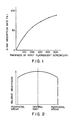
- the X-rays absorbed by an input fluorescent screen with thickness T can be expressed as 1-e - ⁇ T where ⁇ is the X-ray absorption coefficient.
- Fig. 1 shows the relation between the thickness of the input fluorescent screen and the X-ray absorption rate.
- the material of the input fluorescent screen is cesium iodide (CsI) and an energy of X-rays is 60 keV.
- the X-ray absorption rate increases as the thickness increases.
- the distance from the micro part dt to the photoelectric layer is T - t
- the attenuation coefficient of the light in the input fluorescent screen is denoted by ⁇
- the quantity of light that reaches the photoelectric layer of all the light produced by conversion at the micro part dt is: ⁇ e - T ⁇ e - ⁇ (T-t) dt
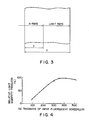
- this method uses a reduced light transmittance for the part of the film at the center of the input fluorescent screen, thereby flattening the output brightness distribution.
- this method is accompanied by a problem that some processes have to be added for vapor-depositing a film having a light transmittance varied in a symmetric form. Since there is a symmetric variation in the light transmittance of the film between the input fluorescent screen and the photoelectric layer, the conditions for forming the photoelectric layer are not uniform. In addition, there is a possibility that a symmetric variation occurs in the variation with time.
- the object of this invention is to provide an X-ray image intensifier capable of flattening the output brightness distribution even when a thick film type input fluorescent screen is used and reducing a variation in the output brightness distribution due to changes in the quality of X-ray.
- an X-ray image intensifier which comprises a vacuum envelope having an input window, through which X-rays are incident on said vacuum envelope; an input fluorescent screen for converting the incident X-rays into light rays, said input fluorescent screen having a first phosphor layer with a first density and a second phosphor layer with a second density higher than the first density, the first phosphor layer being placed on that side of the second phosphor layer which faces said input window, the thickness of the second phosphor layer being greater at peripheral areas than the central part of the input fluorescent screen; a photoelectric layer for converting the light rays into electrons; electrode means forming an electron lens for accelerating and focusing the electrons; and an output fluorescent screen for converting the electrons accelerated and focused by the electron lens into a visible image.
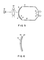
- the numeral 2 indicates a vacuum envelope of an X-ray image intensifier.
- This vacuum envelope 2 has input window 4, through which incident X-rays are cast upon vacuum envelope 2.
- curved substrate 6 is placed where it faces input window 4.
- Input fluorescent screen 8 and photoelectric layer 10 are deposited in the above mentioned order on the side of substrate 6, opposite to input window 4.
- Photoelectric layer 10 converts the X-rays input through input window 4, into light rays.
- Photoelectric layer 10 converts the light rays emanating from input fluorescent screen 8, into electrons.
- Anode 12 and output fluorescent screen 14 are provided on the output side of vacuum envelope 2.
- Focusing electrode 16 is provided along the internal peripheral wall of vacuum envelope 2.
- Anode 12 and focusing electrode 16, together form an electron lens. The electron lens accelerates and focuses the electrons emitted from photoelectric layer 10.
- Output fluorescent screen 14 converts the electrons of which were accelerated and focused by the electron lens, which is composed of anode 12 and focusing electrode 16, into a visible image.
- the light rays are converted into electrons by photoelectric layer 10.
- the electrons are accelerated and focused by an electron lens composed of anode 12 and the focusing electrode 16. Then, the electrons are converted into a visible image by the output fluorescent screen 14.
- the visible image is recorded by means of a TV camera, a cine camera or a spot camera, and the image is then used as a permanent record for medical diagnosis, for example.
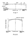
- input fluorescent screen 8 is composed of first phosphor layer 22 having a specified density and second phosphor layer 24 having a density higher than that of first phosphor layer 22.
- Second phosphor layer 24 is provided on the output side of first phosphor layer 22, namely, on the side of first phosphor layer 22 which is opposite to the side which contacts substrate 6.
- first phosphor layer 22 and second phosphor layer 24 of input fluorescent screen 8 consist respectively of long and narrow columnar crystals 22a and 24a formed in a direction perpendicular to input fluorescent screen 8.
- Columnar crystals 22a and 24a are activated cesium iodides (CsI) such as sodium-activated cesium iodide.
- CsI cesium iodides
- Columnar crystals 22a and 24a serve to control the density of input fluorescent screen 8.
- the thickness of second phosphor layer 24 is greater at the peripheral areas than in the central part of input fluorescent screen 8.
- the thickness of first phosphor layer 22 is thinner in the peripheral areas of input fluorescent screen 8 than in the central part.
- the entire input fluorescent screen 8 has a generally uniform thickness extending from its central part toward the peripheral areas.
- the thickness of second phosphor layer 24 is 5 ⁇ m at the central part and 50 ⁇ m in the peripheral areas
- first phosphor layer 22 is 365 ⁇ m at the central part and 220 ⁇ m in the peripheral areas
- the thickness of the whole input fluorescent screen 8 is 370 ⁇ m.
- the phosphor that constitutes the fluorescent screen absorbs X-rays and emits light rays.
- the emitted light rays radiate in all directions.
- the diffusion of these light rays which traveling toward the input fluorescent screen reduces the image resolution.
- the general practice used in preventing this light diffusion is to form long and narrow columnar crystals in a direction perpendicular to the fluorescent screen and make the light rays emanating from the phosphor totally reflected or pass through the interstices of the columnar crystals, thereby attenuating the light rays.
- the density of the phosphor is generally about 0.5% lower in the case where the phosphor is filled without leaving any space.
- the light transmittance, too, is also lower than in the case where the phosphor is filled without leaving any space due to the attenuation of the light described above.
- the fluorescent screen When the thickness of the fluorescent screen is put at 370 ⁇ m and the fluorescent screen is composed of a low density layer with a thickness of 340 ⁇ m consisting of columnar crystals and a high density layer (higher than the lower density layer) with a thickness of 30 ⁇ m, since the difference in density between the low and high density layers is less than 1%, there is little difference in the X-ray absorption rate, but a large difference is recognized in the light transmittance. According to the measurement results, ⁇ is less than 1 ⁇ 10 ⁇ 5 ⁇ m ⁇ 1. In a fluorescent screen made up of these low and high density layers, the light quantity that reaches the photoelectric layer can be expressed as:
- T1 the thickness of the low density layer
- T2 the thickness of the high density layer
- ⁇ the X-ray absorption coefficient of the low and high density layers
- ⁇ 1 the light absorption coefficient of the low density layer
- ⁇ 2 the light absorption coefficient of the low density layer
- e ⁇ 2T2 and e ⁇ 2(T2-t) each can be regarded as 1. Therefore, by solving the above integral equation, the light quantity L can be given as follows.
- the light quantity reaching the photoelectric layer is about 4.5% greater than that in a 370 ⁇ m-thick fluorescent screen of low density, consisting entirely of columnar crystals.
- the light quantity reaching the photoelectric layer can be increased.
- the proportion of the high density layer is increased, the light quantity is further increased. Therefore, for example, if the first phosphor layer thickness T1 is 370 ⁇ m and the second phosphor layer thickness T2 is 0 ⁇ m at the central part of the input fluorescent screen and the first phosphor layer thickness T1 is 320 ⁇ m and the second phosphor layer thickness T2 is 50 ⁇ m in the peripheral areas, the brightness of the peripheral areas can be increased about 7.5%.
- the brightness when the whole fluorescent screen (370 ⁇ m thick) is composed of a phosphor of low density is 0.573, which was obtained by using the equation shown above.
- the brightness is 0.575 when the low density layer thickness T1 is 340 ⁇ m, the high density layer thickness T2 is 30 ⁇ m and the high density layer is provided on the X-ray source side.
- the brightness is 0.600 when the low density layer thickness T1 is 340 ⁇ m, the high density layer thickness T2 is 30 ⁇ m and the high density layer is provided on the output side.
- the brightness can hardly be increased.
- the high density layer is provided on the output side, the brightness can be improved about 5%.
- the X-ray absorption rate varies with the thickness. Therefore, if the above-described construction is used, the brightness can be improved by varying the thicknesses of the low and high density layers constituting the fluorescent screen from the central part to the peripheral areas without varying the thickness of the whole of the fluorescent screen and therefore, the brightness distribution is not changed by changes in the quality of X-ray.
Landscapes
- Physics & Mathematics (AREA)
- Engineering & Computer Science (AREA)
- General Engineering & Computer Science (AREA)
- High Energy & Nuclear Physics (AREA)
- Image-Pickup Tubes, Image-Amplification Tubes, And Storage Tubes (AREA)
Applications Claiming Priority (2)
| Application Number | Priority Date | Filing Date | Title |
|---|---|---|---|
| JP62056740A JP2514952B2 (ja) | 1987-03-13 | 1987-03-13 | X線イメ−ジ管 |
| JP56740/87 | 1987-03-13 |
Publications (3)
| Publication Number | Publication Date |
|---|---|
| EP0282089A2 true EP0282089A2 (fr) | 1988-09-14 |
| EP0282089A3 EP0282089A3 (en) | 1989-03-22 |
| EP0282089B1 EP0282089B1 (fr) | 1991-09-04 |
Family
ID=13035921
Family Applications (1)
| Application Number | Title | Priority Date | Filing Date |
|---|---|---|---|
| EP88103918A Expired EP0282089B1 (fr) | 1987-03-13 | 1988-03-11 | Amplificateur d'images par rayons X |
Country Status (5)
| Country | Link |
|---|---|
| US (1) | US4847482A (fr) |
| EP (1) | EP0282089B1 (fr) |
| JP (1) | JP2514952B2 (fr) |
| CN (1) | CN1012772B (fr) |
| DE (1) | DE3864544D1 (fr) |
Cited By (1)
| Publication number | Priority date | Publication date | Assignee | Title |
|---|---|---|---|---|
| EP0627744A3 (fr) * | 1993-06-01 | 1995-03-01 | Du Pont | Système radiologique amélioré utilisant des matériaux luminescents de densités différentes. |
Families Citing this family (5)
| Publication number | Priority date | Publication date | Assignee | Title |
|---|---|---|---|---|
| JPH02152143A (ja) * | 1988-12-02 | 1990-06-12 | Toshiba Corp | X線イメージ管及びその製造方法 |
| US5029247A (en) * | 1989-06-20 | 1991-07-02 | Kabushiki Kaisha Toshiba | X-ray image intensifier and method of manufacturing input screen |
| FR2681727B1 (fr) * | 1991-09-20 | 1993-11-05 | Thomson Tubes Electroniques | Tube intensificateur d'image a correction de brillance. |
| WO1998012731A1 (fr) * | 1996-09-18 | 1998-03-26 | Kabushiki Kaisha Toshiba | Tube a image radiologique et son procede de fabrication |
| JP2011137665A (ja) * | 2009-12-26 | 2011-07-14 | Canon Inc | シンチレータパネル及び放射線撮像装置とその製造方法、ならびに放射線撮像システム |
Family Cites Families (10)
| Publication number | Priority date | Publication date | Assignee | Title |
|---|---|---|---|---|
| BE518747A (fr) * | 1952-03-29 | |||
| US3716713A (en) * | 1969-01-09 | 1973-02-13 | Varian Associates | Input screen for image devices having reduced sensitivity in the cental region |
| JPS51131264A (en) * | 1975-05-10 | 1976-11-15 | Toshiba Corp | The input of x-ray fluorescence intensifying tube |
| JPS5927072B2 (ja) * | 1977-02-21 | 1984-07-03 | 株式会社東芝 | 像増強管用入力面 |
| JPS53102663A (en) * | 1977-02-21 | 1978-09-07 | Toshiba Corp | Manufacture for input surface of image intensifier tube |
| JPS5631049A (en) * | 1979-08-23 | 1981-03-28 | Atsuko Inoue | Bead knitting method |
| FR2467481A1 (fr) * | 1979-10-12 | 1981-04-17 | Thomson Csf | Ecran scintillateur pour tube intensificateur d'image radiologique, son procede de fabrication, et tube incorporant un tel ecran |
| US4437011A (en) * | 1980-06-16 | 1984-03-13 | Tokyo Shibaura Denki Kabushiki Kaisha | Radiation excited phosphor screen and method for manufacturing the same |
| FR2545270B1 (fr) * | 1983-04-29 | 1985-12-27 | Thomson Csf | Intensificateur d'images radiologiques et application a un systeme de radiologie numerique |
| JPH0754675B2 (ja) * | 1986-03-31 | 1995-06-07 | 株式会社東芝 | X線イメ−ジインテンシフアイア |
-
1987
- 1987-03-13 JP JP62056740A patent/JP2514952B2/ja not_active Expired - Lifetime
-
1988
- 1988-03-11 US US07/167,244 patent/US4847482A/en not_active Expired - Lifetime
- 1988-03-11 EP EP88103918A patent/EP0282089B1/fr not_active Expired
- 1988-03-11 DE DE8888103918T patent/DE3864544D1/de not_active Expired - Lifetime
- 1988-03-12 CN CN88101359.5A patent/CN1012772B/zh not_active Expired
Cited By (1)
| Publication number | Priority date | Publication date | Assignee | Title |
|---|---|---|---|---|
| EP0627744A3 (fr) * | 1993-06-01 | 1995-03-01 | Du Pont | Système radiologique amélioré utilisant des matériaux luminescents de densités différentes. |
Also Published As
| Publication number | Publication date |
|---|---|
| CN88101359A (zh) | 1988-09-28 |
| CN1012772B (zh) | 1991-06-05 |
| EP0282089B1 (fr) | 1991-09-04 |
| DE3864544D1 (de) | 1991-10-10 |
| JPS63224133A (ja) | 1988-09-19 |
| EP0282089A3 (en) | 1989-03-22 |
| US4847482A (en) | 1989-07-11 |
| JP2514952B2 (ja) | 1996-07-10 |
Similar Documents
| Publication | Publication Date | Title |
|---|---|---|
| US4437011A (en) | Radiation excited phosphor screen and method for manufacturing the same | |
| US2555423A (en) | Image intensifying tube | |
| US4208577A (en) | X-ray tube having scintillator-photocathode segments aligned with phosphor segments of its display screen | |
| US4140900A (en) | Panel type x-ray image intensifier tube and radiographic camera system | |
| US3693018A (en) | X-ray image intensifier tubes having the photo-cathode formed directly on the pick-up screen | |
| US4300046A (en) | Panel type X-ray image intensifier tube and radiographic camera system | |
| US4255666A (en) | Two stage, panel type x-ray image intensifier tube | |
| EP0282089B1 (fr) | Amplificateur d'images par rayons X | |
| EP0199426B1 (fr) | Intensificateur d'image de rayonnement | |
| US4820926A (en) | Radiation conversion screen | |
| GB1592835A (en) | X-ray image intensifier tube | |
| US7022994B2 (en) | Radiation converter | |
| US4447721A (en) | Panel type X-ray image intensifier tube and radiographic camera system | |
| US2690516A (en) | Method and device for producing neutron images | |
| US5811932A (en) | X-ray detector having an entrance section including a low energy x-ray filter preceding a conversion layer | |
| EP0667635B1 (fr) | Tube intensificateur d'image | |
| JPS61230241A (ja) | X線像増倍管 | |
| EP0399378B1 (fr) | Intensificateur d'images de rayons X | |
| JPS59207551A (ja) | X線像増倍管 | |
| US4880965A (en) | X-ray image intensifier having variable-size fluorescent crystals | |
| JPS6155729B2 (fr) | ||
| JP3007535B2 (ja) | X線イメージ管 | |
| Garrett et al. | Concepts and implementations in X-ray intensification | |
| JP2798867B2 (ja) | X線イメージ管 | |
| JPH05190126A (ja) | X線イメージ管 |
Legal Events
| Date | Code | Title | Description |
|---|---|---|---|
| PUAI | Public reference made under article 153(3) epc to a published international application that has entered the european phase |
Free format text: ORIGINAL CODE: 0009012 |
|
| 17P | Request for examination filed |
Effective date: 19880408 |
|
| AK | Designated contracting states |
Kind code of ref document: A2 Designated state(s): DE FR GB |
|
| PUAL | Search report despatched |
Free format text: ORIGINAL CODE: 0009013 |
|
| AK | Designated contracting states |
Kind code of ref document: A3 Designated state(s): DE FR GB |
|
| 17Q | First examination report despatched |
Effective date: 19901207 |
|
| GRAA | (expected) grant |
Free format text: ORIGINAL CODE: 0009210 |
|
| AK | Designated contracting states |
Kind code of ref document: B1 Designated state(s): DE FR GB |
|
| REF | Corresponds to: |
Ref document number: 3864544 Country of ref document: DE Date of ref document: 19911010 |
|
| ET | Fr: translation filed | ||
| PLBE | No opposition filed within time limit |
Free format text: ORIGINAL CODE: 0009261 |
|
| STAA | Information on the status of an ep patent application or granted ep patent |
Free format text: STATUS: NO OPPOSITION FILED WITHIN TIME LIMIT |
|
| 26N | No opposition filed | ||
| REG | Reference to a national code |
Ref country code: GB Ref legal event code: 746 Effective date: 19981008 |
|
| REG | Reference to a national code |
Ref country code: FR Ref legal event code: D6 |
|
| REG | Reference to a national code |
Ref country code: GB Ref legal event code: IF02 |
|
| PGFP | Annual fee paid to national office [announced via postgrant information from national office to epo] |
Ref country code: GB Payment date: 20070307 Year of fee payment: 20 |
|
| PGFP | Annual fee paid to national office [announced via postgrant information from national office to epo] |
Ref country code: DE Payment date: 20070308 Year of fee payment: 20 |
|
| REG | Reference to a national code |
Ref country code: GB Ref legal event code: PE20 Expiry date: 20080310 |
|
| PGFP | Annual fee paid to national office [announced via postgrant information from national office to epo] |
Ref country code: FR Payment date: 20070308 Year of fee payment: 20 |
|
| PG25 | Lapsed in a contracting state [announced via postgrant information from national office to epo] |
Ref country code: GB Free format text: LAPSE BECAUSE OF EXPIRATION OF PROTECTION Effective date: 20080310 |