EP0282201B1 - Procédé pour réaliser des patrons - Google Patents
Procédé pour réaliser des patrons Download PDFInfo
- Publication number
- EP0282201B1 EP0282201B1 EP88301564A EP88301564A EP0282201B1 EP 0282201 B1 EP0282201 B1 EP 0282201B1 EP 88301564 A EP88301564 A EP 88301564A EP 88301564 A EP88301564 A EP 88301564A EP 0282201 B1 EP0282201 B1 EP 0282201B1
- Authority
- EP
- European Patent Office
- Prior art keywords
- film
- forming method
- pattern forming
- light
- light beam
- Prior art date
- Legal status (The legal status is an assumption and is not a legal conclusion. Google has not performed a legal analysis and makes no representation as to the accuracy of the status listed.)
- Expired - Lifetime
Links
Images


Classifications
-
- H—ELECTRICITY
- H10—SEMICONDUCTOR DEVICES; ELECTRIC SOLID-STATE DEVICES NOT OTHERWISE PROVIDED FOR
- H10P—GENERIC PROCESSES OR APPARATUS FOR THE MANUFACTURE OR TREATMENT OF DEVICES COVERED BY CLASS H10
- H10P76/00—Manufacture or treatment of masks on semiconductor bodies, e.g. by lithography or photolithography
- H10P76/20—Manufacture or treatment of masks on semiconductor bodies, e.g. by lithography or photolithography of masks comprising organic materials
- H10P76/204—Manufacture or treatment of masks on semiconductor bodies, e.g. by lithography or photolithography of masks comprising organic materials of organic photoresist masks
- H10P76/2041—Photolithographic processes
-
- G—PHYSICS
- G03—PHOTOGRAPHY; CINEMATOGRAPHY; ANALOGOUS TECHNIQUES USING WAVES OTHER THAN OPTICAL WAVES; ELECTROGRAPHY; HOLOGRAPHY
- G03F—PHOTOMECHANICAL PRODUCTION OF TEXTURED OR PATTERNED SURFACES, e.g. FOR PRINTING, FOR PROCESSING OF SEMICONDUCTOR DEVICES; MATERIALS THEREFOR; ORIGINALS THEREFOR; APPARATUS SPECIALLY ADAPTED THEREFOR
- G03F7/00—Photomechanical, e.g. photolithographic, production of textured or patterned surfaces, e.g. printing surfaces; Materials therefor, e.g. comprising photoresists; Apparatus specially adapted therefor
- G03F7/20—Exposure; Apparatus therefor
- G03F7/2051—Exposure without an original mask, e.g. using a programmed deflection of a point source, by scanning, by drawing with a light beam, using an addressed light or corpuscular source
- G03F7/2053—Exposure without an original mask, e.g. using a programmed deflection of a point source, by scanning, by drawing with a light beam, using an addressed light or corpuscular source using a laser
-
- G—PHYSICS
- G03—PHOTOGRAPHY; CINEMATOGRAPHY; ANALOGOUS TECHNIQUES USING WAVES OTHER THAN OPTICAL WAVES; ELECTROGRAPHY; HOLOGRAPHY
- G03F—PHOTOMECHANICAL PRODUCTION OF TEXTURED OR PATTERNED SURFACES, e.g. FOR PRINTING, FOR PROCESSING OF SEMICONDUCTOR DEVICES; MATERIALS THEREFOR; ORIGINALS THEREFOR; APPARATUS SPECIALLY ADAPTED THEREFOR
- G03F7/00—Photomechanical, e.g. photolithographic, production of textured or patterned surfaces, e.g. printing surfaces; Materials therefor, e.g. comprising photoresists; Apparatus specially adapted therefor
- G03F7/004—Photosensitive materials
- G03F7/09—Photosensitive materials characterised by structural details, e.g. supports, auxiliary layers
- G03F7/091—Photosensitive materials characterised by structural details, e.g. supports, auxiliary layers characterised by antireflection means or light filtering or absorbing means, e.g. anti-halation, contrast enhancement
-
- G—PHYSICS
- G03—PHOTOGRAPHY; CINEMATOGRAPHY; ANALOGOUS TECHNIQUES USING WAVES OTHER THAN OPTICAL WAVES; ELECTROGRAPHY; HOLOGRAPHY
- G03F—PHOTOMECHANICAL PRODUCTION OF TEXTURED OR PATTERNED SURFACES, e.g. FOR PRINTING, FOR PROCESSING OF SEMICONDUCTOR DEVICES; MATERIALS THEREFOR; ORIGINALS THEREFOR; APPARATUS SPECIALLY ADAPTED THEREFOR
- G03F7/00—Photomechanical, e.g. photolithographic, production of textured or patterned surfaces, e.g. printing surfaces; Materials therefor, e.g. comprising photoresists; Apparatus specially adapted therefor
- G03F7/004—Photosensitive materials
- G03F7/09—Photosensitive materials characterised by structural details, e.g. supports, auxiliary layers
- G03F7/105—Photosensitive materials characterised by structural details, e.g. supports, auxiliary layers having substances, e.g. indicators, for forming visible images
-
- G—PHYSICS
- G03—PHOTOGRAPHY; CINEMATOGRAPHY; ANALOGOUS TECHNIQUES USING WAVES OTHER THAN OPTICAL WAVES; ELECTROGRAPHY; HOLOGRAPHY
- G03F—PHOTOMECHANICAL PRODUCTION OF TEXTURED OR PATTERNED SURFACES, e.g. FOR PRINTING, FOR PROCESSING OF SEMICONDUCTOR DEVICES; MATERIALS THEREFOR; ORIGINALS THEREFOR; APPARATUS SPECIALLY ADAPTED THEREFOR
- G03F7/00—Photomechanical, e.g. photolithographic, production of textured or patterned surfaces, e.g. printing surfaces; Materials therefor, e.g. comprising photoresists; Apparatus specially adapted therefor
- G03F7/20—Exposure; Apparatus therefor
- G03F7/2022—Multi-step exposure, e.g. hybrid; backside exposure; blanket exposure, e.g. for image reversal; edge exposure, e.g. for edge bead removal; corrective exposure
Definitions
- This invention relates to a pattern forming method and, more particularly to a pattern forming method for a new and simple pattern forming which is capable of providing a superfine pattern by a simple process.
- WO-A-8601313 An example of a process for forming a layer of patterned photoresist on a semiconductor substrate is shown in WO-A-8601313. According to this process a selected area of a thin layer of polymeric photoresist is exposed to radiation to convert it to monomeric form. The unexposed part of the photoresist is then hardened and the exposed part is removed, leaving a pattern of unexposed photoresist.
- JP-A-6105230 discloses another pattern forming method in which a pattern is formed in a layer of photoresist by ion implantation, the ion implanted areas then acting as a mask in a subsequent exposure to ultraviolet radiation. Exposed parts of the photoresist are then removed leaving only the implanted areas to form the pattern.
- the present invention provides a reverse process in which the portion of an organic thin film which is to form the required pattern is exposed to radiation, and the remaining part is removed.
- a first aspect of the present invention provides a pattern forming method comprising: forming an organic thin film on a substrate, the film having chemical properties which change with photochemical reactions in the vicinity of the surface of the film in response to a first light beam directed at the surface of the film; and selectively exposing the surface of the film, according to a predetermined pattern, to said first light beam, whereby to cause said change in properties in a selected area of said film; characterised by the film being substantially opaque to said first light beam and substantially transparent to a second energy beam whereby said exposing step forms an area for selectively absorbing said second energy beam on the surface of the film; exposing the entire surface of said organic thin film to said second energy beam; and developing the portion of the film exposed to said second energy beam excluding the portion of the film exposed to the first light beam.
- the organic coat film material is, for example, made of alkaline soluble resin primarily, containing, furthermore, an organic material made of aromatic azide compound which chemically changes at the wavelength of first exposure and diazo compound which chemically changes at the wavelength of second exposure.
- the present invention provides a pattern forming method comprising: forming an organic thin film on a substrate, the
- the pattern forming method of this invention realizes the resist process making use of only the advantageous points of all of MLR, CEL, PCM, IR and other methods.
- the primary energy beam exposure for example, only the vicinity of the surface of positive resist is used, and it is exposed selectively by deep UV light (for example, KrF excimer light; 248 nm) so as to degenerate only the vicinity of surface of said resist.
- deep UV light for example, KrF excimer light; 248 nm
- the above degenerated portion is selectively stained with a chemical substance which absorbs the light of secondary energy beam exposure, for example, dyestuff.
- the entire surface is exposed by, for example, UV light which is excellent in transmissivity to the resist as secondary energy beam, and the positive resist is developed and removed, leaving only the already stained portion.
- an organic thin film 2 is formed on an arbitrary substrate (for example, a semiconductor substrate) 1 by coating with an organic coating material in a thickness of 1 to 2 microns meter.
- Said organic coating material is primarily composed of alkaline soluble resin (for example, phenol novolak resin), and contains, as photosensitizers, diazo compound (for example, 1,2-naphthoquinone diazide sulfonic chloride) and aromatic azide compound (for example, 2-phenylamino-5-azidebenzoic acid).
- diazo compound for example, 1,2-naphthoquinone diazide sulfonic chloride
- aromatic azide compound for example, 2-phenylamino-5-azidebenzoic acid
- numeral 4 denotes a photo mask for selective exposure.
- the principal component of the organic thin film 2 absorbs the majority of the far ultraviolet ray, only the surface layer in a thickness of 0.1 to 0.2 microns meter of the organic thin film 2 is exposed in a pattern, and a very thin exposure part 5 is formed only on the surface. Therefore, in this step, the same effect as in the multilayer resist is obtained, that is, the effect is the same as when thin resists are overlaid and only the top layer resist is exposed selectively. Namely, an exposure apparatus with shallow focal depth and high resolution can be used, and a sharp superfine pattern of 0.5 micron meter or less with a high resolution can be obtained (Fig. 3).
- the aromatic azide compound for example, 2-phenylamino-5-azidebenzoic acid
- far ultraviolet light for example, excimer laser light
- the extremely thin exposure part 5 of the surface only above forms a colored part 6 which is colored by said compound.
- the colored part 6 absorbs all light with wavelength of at least 450 nm or less (Fig. 4). Therefore, when the entire surface is exposed by using light 7 with longer wavelength than said far ultraviolet light in a second exposure, for example, light with wavelength of 450 nm or less (for instance, g-ray of 436 nm), only the uncolored portion 8 of the organic thin film 2 is selectively exposed (Fig. 5).
- the uncolored part 8 which is in contact with the colored part 6 is exposed, and this is a contact exposure of so-called mask contact type. Therefore, pattern exposure of high fidelity to the mask and high precision may be performed. That is, in this step, the three effects of the CEL method, PCM method, and IR method are taken in at the same time.
- KrF excimer laser light was used in the first exposure and g-ray as the second exposure, but the wavelengths of the first and second exposures may freely changed by the combination of light absorbing regions of the diazo compound and aromatic azide compound which are photosensitizers making up the organic coating material.
- the colored part was formed selectively only on the exposed part, but, to the contrary, it is evident that the same effect is obtained, except that the pattern is inverted, when only the exposed part is decolored by causing chemical change on the colored part in the vicinity of the surface of the organic thin film by the wavelength of the first exposure, using an organic film on which a colored part is preliminarily formed entirely.
- the light of the first exposure is not limited to excimer laser light, but X-ray, electron beam, ion beam and others may be used
- the light of the second exposure is not limited to g-ray, but i-ray, visible ray, soft X-ray and others may be used.
- the exposure apparatus in the pattern-shaped first exposure, since only the surface portion of the organic thin film 2 is used, the exposure apparatus is widened in the aperture and shortened in the wavelength, and it is sufficiently usable if the focal depth becomes shallow, so that the resolution of the apparatus can be fully exhibited.
- the pattern forming method of this embodiment does not require formation of photo bleaching film on the resist surface as required in the conventional contrast enhanced method (CEL method) process, so that the exposure time is significantly shortened, while the contrast is sufficient and coating is needed only in one step.
- CEL method contrast enhanced method
- the pattern forming method of this embodiment is capable of forming a light absorption layer in a pattern shape of high contrast on the surface of resist without coating in two layers, so that the resolution of the resist pattern may be greatly improved. And many other effects are obtained.
- the pattern forming method and pattern forming materials of this embodiment are effective to obtain a sufficiently high resolution, being applied to an exposure apparatus with shallow focal depth, such as excimer laser stepper, without making and drastic modification as compared with the conventional photo resist process technology.
- an arbitrary substrate for example, a semiconductor substrate (e.g. Si substrate) 10 on which a semiconductor wafer, that is, SiO2 40 is formed is coated with an ordinary positive resist 11 [for example, AZ1400, AZ4000, AZ5200 (all made by Hoechst)] in a thickness of 1 to 2 »m.
- an ordinary positive resist 11 for example, AZ1400, AZ4000, AZ5200 (all made by Hoechst)
- deep UV light (far ultraviolet ray, such as KrF excimer light) 12 is selectively emitted for a short time to expose the vicinity of the surface of the positive resist 11 selectively (Fig. 8).
- the main polymer of the positive resist 11 absorpts the majority of deep UV light, if slightly overexposed, the positive resist 11 is selectively exposed in a pattern shape only in the surface layer in a thickness of 0.1 to 0.2 »m, so that an extremely thin exposure pattern 20 is formed. Therefore, in this step, the same effect as in the multilayer resist, that is, lamination of thin resist layers and selective exposure of only the top layer resist, will be obtained. Namely, an exposure apparatus of shallow focal depth and high resolution can be used, and a sharp and high resolution superfine pattern 20 of 0.5 »m or less in width may be obtained.
- the surface layer 20 of the positive resist selectively exposed in the above step contains, as a photosensitive material, a reagent including a group of naphthoquinone diazide compound, and photoreaction of formula (3) occurs only by exposure.
- the alkaline dyestuff such as fuchsine for red color, auramine for yellow, and aniline black for black
- a stained layer 30 is formed (Fig. 9).
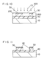
- the alkaline dyes of red, yellow and black absorb all light with wavelength of at least 450 nm or less. Therefore, in the secondary exposure, when the entire surface is exposed by using light with longer wavelength than that of above deep UV light, for example, light 13 with wavelength of 450 nm or less, only the unstained portion 200 of the resist 11 can be selectively exposed (Fig. 10). That is, in this step, the three effects of CEL method, PCM method and IR method are taken in simultaneously.
- a high resolution resist pattern 14 of about 0.5 »m opposite to the mask pattern may be used by using the positive resist (Fig. 11).
- KrF excimer light was used in the first exposure and UV light in the second exposure, but depending on the selection of resist, light of same wavelength may be used in the first and second exposures.
- alkaline dyes were used, but it is obvious that they are not limitative as far as it is possible to absorb the light of second exposure and deposit selectively on the exposure pattern part, and for example aniline may be used because it can absorb light of g-ray.
- the light of the first exposure is not limited to excimer laser light, by X-ray, electron beam, ion beam and others may be used
- the light of the second exposure is not limited to g-ray, but i-ray, visible ray, soft X-ray and others may be used.
- the organic thin film is not limited to the positive resist, and any other material such as polycarbonate resin can be used as far as it can cause chemical reaction by the first energy beam and selectively deposit that substance that does not absorb or pass the second energy beam.
- the pattern shaped primary exposure is used only on the resist surface, it is sufficiently usable if the exposure apparatus is higher in NA and shorter in wavelength, and shallow in the focal depth, whereas the resolution of the apparatus can be fully exhibited.
Landscapes
- Physics & Mathematics (AREA)
- General Physics & Mathematics (AREA)
- Engineering & Computer Science (AREA)
- Architecture (AREA)
- Structural Engineering (AREA)
- Optics & Photonics (AREA)
- Exposure And Positioning Against Photoresist Photosensitive Materials (AREA)
- Photosensitive Polymer And Photoresist Processing (AREA)
- Exposure Of Semiconductors, Excluding Electron Or Ion Beam Exposure (AREA)
Claims (15)
- Procédé de formation d'un motif, comprenant :
la formation d'un film organique mince (2) sur un substrat (1), le film (2) ayant des propriétés chimiques qui changent avec les réactions photochimiques du voisinage de la surface du film sous l'action d'un premier faisceau lumineux (3) dirigé à la surface du film, et
l'exposition sélective de la surface du film (2), avec un motif prédéterminé, au premier faisceau lumineux (3), de manière que le changement de propriétés soit provoqué dans une zone choisie du film,
caractérisé en ce que
le film est pratiquement opaque au premier faisceau lumineux et pratiquement transparent au second faisceau d'énergie, si bien que l'étape d'exposition forme une zone (6) d'absorption sélective du second faisceau d'énergie (7) à la surface du film,
toute la surface du film organique mince (2) est exposée au second faisceau d'énergie, et
la partie (8) du film (2) exposée au second faisceau d'énergie (7) est développée à l'exclusion de la partie du film exposée au premier faisceau lumineux. - Procédé de formation d'un motif selon la revendication 1, dans lequel le film organique mince (2) est essentiellement composé d'une résine soluble dans une matière alcaline, et contient une matière organique qui change chimiquement à la longueur d'onde du premier faisceau lumineux (3) et une matière organique qui change chimiquement à la longueur d'onde du second faisceau d'énergie (7).
- Procédé de formation d'un motif selon la revendication 2, dans lequel la matière organique qui est changée par la lumière à la longueur d'onde du premier faisceau lumineux (3) contient un composé d'azide aromatique et cette matière organique est composée d'une matière organique qui est modifiée chimiquement par la lumière à la longueur d'onde du premier faisceau lumineux (3) en une substance assurant l'absorption de la région des longueurs d'onde du second faisceau d'énergie (7).
- Procédé de formation d'un motif selon la revendication 3, dans lequel le composé d'azide aromatique est l'acide 2-phénylamino-S-azidebenzoïque.
- Procédé de formation d'un motif selon la revendication 2, 3 ou 4, dans lequel la matière organique qui est changée par la lumière à la longueur d'onde du second faisceau d'énergie (7) est un composé diazoïque.
- Procédé de formation d'un motif selon la revendication 5, dans lequel le composé diazoïque est le chlorure sulfonique de 1,2-naphtoquinonediazide.
- Procédé de formation d'un motif selon l'une quelconque des revendications précédentes, dans lequel la longueur d'onde du premier faisceau lumineux est supérieure à celle du second faisceau d'énergie.
- Procédé de formation d'un motif selon l'une quelconque des revendications précédentes, dans lequel le premier et le second faisceau d'énergie sont des rayonnements ultraviolets.
- Procédé de formation d'un motif selon l'une quelconque des revendications précédentes, dans lequel le premier faisceau d'énergie est la lumière d'un laser à excimère dans l'ultraviolet lointain.
- Procédé de formation d'un motif comprenant :
la formation d'un film organique mince (11) sur un substrat (10), le film (11) ayant des propriétés chimiques qui changent avec les réactions chimiques au voisinage de la surface du film sous l'action d'un premier faisceau lumineux (12) dirigé à la surface du film, et
l'exposition sélective de la surface du film (10), suivant un motif prédéterminé, par le premier faisceau lumineux (12) afin que le changement de propriétés chimiques soit provoqué dans une zone choisie (20) du film (10),
caractérisé par
la coloration de la partie (20) du film exposée au premier faisceau lumineux (12),
l'exposition de toute la surface du film organique mince (11) à un second faisceau d'énergie (13) avec la partie colorée (30) agissant comme masque, et
le développement de la partie (200) du film organique (11) exposée au second faisceau d'énergie (13), à l'exclusion des zones exposées au premier faisceau lumineux (12). - Procédé de formation d'un motif selon la revendication 10, dans lequel le film organique contenant un polymère principal qui absorbe le premier faisceau lumineux est formé d'une matière de réserve positive, et la partie colorée est formée par imprégnation par une matière de coloration.
- Procédé de formation d'un motif selon la revendication 10 ou 11, dans lequel le film organique mince est une matière de réserve positive,
- Procédé de formation d'un motif selon la revendication 10, 11 ou 12, dans lequel la substance qui absorbe le faisceau d'énergie est un colorant.
- Procédé de formation d'un motif selon la revendication 13, dans lequel le colorant est un colorant alcalin.
- Procédé de formation d'un motif selon la revendication 10, 11, 12 ou 13, dans lequel la matière de réserve contient un groupe

Applications Claiming Priority (4)
| Application Number | Priority Date | Filing Date | Title |
|---|---|---|---|
| JP53302/87 | 1987-03-09 | ||
| JP62053302A JP2553545B2 (ja) | 1987-03-09 | 1987-03-09 | パタ−ン形成方法 |
| JP309055/87 | 1987-12-07 | ||
| JP62309055A JP2653072B2 (ja) | 1987-12-07 | 1987-12-07 | パターン形成方法 |
Publications (3)
| Publication Number | Publication Date |
|---|---|
| EP0282201A2 EP0282201A2 (fr) | 1988-09-14 |
| EP0282201A3 EP0282201A3 (fr) | 1991-04-10 |
| EP0282201B1 true EP0282201B1 (fr) | 1994-06-15 |
Family
ID=26394017
Family Applications (1)
| Application Number | Title | Priority Date | Filing Date |
|---|---|---|---|
| EP88301564A Expired - Lifetime EP0282201B1 (fr) | 1987-03-09 | 1988-02-24 | Procédé pour réaliser des patrons |
Country Status (3)
| Country | Link |
|---|---|
| EP (1) | EP0282201B1 (fr) |
| KR (1) | KR920003315B1 (fr) |
| DE (1) | DE3850151T2 (fr) |
Families Citing this family (6)
| Publication number | Priority date | Publication date | Assignee | Title |
|---|---|---|---|---|
| EP0394738A3 (fr) * | 1989-04-24 | 1991-03-27 | Siemens Aktiengesellschaft | Système photoréserve à couches multiples |
| JP2544006B2 (ja) * | 1990-06-14 | 1996-10-16 | 株式会社東芝 | 半導体装置の製造方法 |
| EP0559934A1 (fr) * | 1992-03-11 | 1993-09-15 | International Business Machines Corporation | Méthode et appareil pour création de structures avec image inversée dans l'UV lointain |
| KR0172237B1 (ko) * | 1995-06-26 | 1999-03-30 | 김주용 | 반도체 소자의 미세패턴 형성방법 |
| JP2004283065A (ja) * | 2003-03-20 | 2004-10-14 | Ushio Inc | 化学走性機能制御膜の製造方法および人工材料並びに人工材料の製造方法 |
| CN101312113B (zh) * | 2007-05-23 | 2010-06-16 | 中芯国际集成电路制造(上海)有限公司 | 图形的形成方法 |
Family Cites Families (4)
| Publication number | Priority date | Publication date | Assignee | Title |
|---|---|---|---|---|
| US3784378A (en) * | 1971-10-18 | 1974-01-08 | Du Pont | Double-exposure method for producing reverse images in photopolymers |
| DE3248246A1 (de) * | 1982-12-28 | 1984-06-28 | Basf Ag, 6700 Ludwigshafen | Positiv arbeitendes verfahren zur herstellung von relief- und druckformen |
| DE3582491D1 (de) * | 1984-08-13 | 1991-05-16 | Ncr Co | Verfahren zur herstellung von dessinierten photoschutzlackschichten. |
| US4810601A (en) * | 1984-12-07 | 1989-03-07 | International Business Machines Corporation | Top imaged resists |
-
1988
- 1988-02-24 EP EP88301564A patent/EP0282201B1/fr not_active Expired - Lifetime
- 1988-02-24 DE DE3850151T patent/DE3850151T2/de not_active Expired - Fee Related
- 1988-03-08 KR KR1019880002382A patent/KR920003315B1/ko not_active Expired
Also Published As
| Publication number | Publication date |
|---|---|
| DE3850151T2 (de) | 1995-01-12 |
| EP0282201A3 (fr) | 1991-04-10 |
| EP0282201A2 (fr) | 1988-09-14 |
| KR880011900A (ko) | 1988-10-31 |
| KR920003315B1 (ko) | 1992-04-27 |
| DE3850151D1 (de) | 1994-07-21 |
Similar Documents
| Publication | Publication Date | Title |
|---|---|---|
| US4672021A (en) | Contrast enhancement layer composition with naphthoquinone diazide, indicator dye and polymeric binder | |
| KR100798969B1 (ko) | 포토마스크, 그 제조방법, 패턴형성방법 및 반도체장치의제조방법 | |
| JPS6113746B2 (fr) | ||
| US5718991A (en) | Method for making photomasks having regions of different light transmissivities | |
| US4311773A (en) | Method of producing color filters | |
| US6245492B1 (en) | Photoresist system and process for aerial image enhancement | |
| US20070105043A1 (en) | Photosensitive coating for enhancing a contrast of a photolithographic exposure | |
| US4777111A (en) | Photographic element with diazo contrast enhancement layer and method of producing image in underlying photoresist layer of element | |
| JP2004526993A5 (fr) | ||
| US7022452B2 (en) | Contrast enhanced photolithography | |
| JP2543195B2 (ja) | 微細レジストパタ―ンの形成方法 | |
| US5443931A (en) | Photo mask and repair method of the same | |
| EP0282201A2 (fr) | Procédé pour réaliser des patrons | |
| US4804614A (en) | Photoresist process of fabricating microelectronic circuits using water processable diazonium compound containing contrast enhancement layer | |
| KR100396193B1 (ko) | 패턴의 형성방법 | |
| EP0113033A2 (fr) | Procédé pour l'obtention de réserves | |
| JPS60238829A (ja) | パタ−ン形成方法 | |
| EP0154932A2 (fr) | Procédé photolaque à plusieurs couches | |
| JP2553545B2 (ja) | パタ−ン形成方法 | |
| JP2588192B2 (ja) | パタ−ン形成方法 | |
| JPH06267890A (ja) | 小さなマスク開口部を製造するためのリソグラフィー方法およびその製造物 | |
| KR0128833B1 (ko) | 반도체 소자의 미세패턴 제조방법 | |
| JP2653072B2 (ja) | パターン形成方法 | |
| KR970004421B1 (ko) | 반도체 노광장치 | |
| KR100272519B1 (ko) | 반도체소자의 패터닝방법 |
Legal Events
| Date | Code | Title | Description |
|---|---|---|---|
| PUAI | Public reference made under article 153(3) epc to a published international application that has entered the european phase |
Free format text: ORIGINAL CODE: 0009012 |
|
| AK | Designated contracting states |
Kind code of ref document: A2 Designated state(s): DE FR GB |
|
| PUAL | Search report despatched |
Free format text: ORIGINAL CODE: 0009013 |
|
| AK | Designated contracting states |
Kind code of ref document: A3 Designated state(s): DE FR GB |
|
| 17P | Request for examination filed |
Effective date: 19910723 |
|
| 17Q | First examination report despatched |
Effective date: 19920219 |
|
| GRAA | (expected) grant |
Free format text: ORIGINAL CODE: 0009210 |
|
| AK | Designated contracting states |
Kind code of ref document: B1 Designated state(s): DE FR GB |
|
| REF | Corresponds to: |
Ref document number: 3850151 Country of ref document: DE Date of ref document: 19940721 |
|
| ET | Fr: translation filed | ||
| PLBE | No opposition filed within time limit |
Free format text: ORIGINAL CODE: 0009261 |
|
| STAA | Information on the status of an ep patent application or granted ep patent |
Free format text: STATUS: NO OPPOSITION FILED WITHIN TIME LIMIT |
|
| 26N | No opposition filed | ||
| REG | Reference to a national code |
Ref country code: GB Ref legal event code: 746 Effective date: 19951123 |
|
| REG | Reference to a national code |
Ref country code: FR Ref legal event code: D6 |
|
| REG | Reference to a national code |
Ref country code: GB Ref legal event code: IF02 |
|
| PGFP | Annual fee paid to national office [announced via postgrant information from national office to epo] |
Ref country code: FR Payment date: 20040210 Year of fee payment: 17 |
|
| PGFP | Annual fee paid to national office [announced via postgrant information from national office to epo] |
Ref country code: GB Payment date: 20040218 Year of fee payment: 17 |
|
| PGFP | Annual fee paid to national office [announced via postgrant information from national office to epo] |
Ref country code: DE Payment date: 20040304 Year of fee payment: 17 |
|
| PG25 | Lapsed in a contracting state [announced via postgrant information from national office to epo] |
Ref country code: GB Free format text: LAPSE BECAUSE OF NON-PAYMENT OF DUE FEES Effective date: 20050224 |
|
| PG25 | Lapsed in a contracting state [announced via postgrant information from national office to epo] |
Ref country code: DE Free format text: LAPSE BECAUSE OF NON-PAYMENT OF DUE FEES Effective date: 20050901 |
|
| GBPC | Gb: european patent ceased through non-payment of renewal fee |
Effective date: 20050224 |
|
| PG25 | Lapsed in a contracting state [announced via postgrant information from national office to epo] |
Ref country code: FR Free format text: LAPSE BECAUSE OF NON-PAYMENT OF DUE FEES Effective date: 20051031 |
|
| REG | Reference to a national code |
Ref country code: FR Ref legal event code: ST Effective date: 20051031 |