EP0282226A2 - Verbindungssystem hoher Geschwindigkeit mit feuerfesten Kontakten vom "non-dogbone-Typ" und ein aktiver elektromigrationsunterdrückender Mechanismus - Google Patents
Verbindungssystem hoher Geschwindigkeit mit feuerfesten Kontakten vom "non-dogbone-Typ" und ein aktiver elektromigrationsunterdrückender Mechanismus Download PDFInfo
- Publication number
- EP0282226A2 EP0282226A2 EP88301827A EP88301827A EP0282226A2 EP 0282226 A2 EP0282226 A2 EP 0282226A2 EP 88301827 A EP88301827 A EP 88301827A EP 88301827 A EP88301827 A EP 88301827A EP 0282226 A2 EP0282226 A2 EP 0282226A2
- Authority
- EP
- European Patent Office
- Prior art keywords
- refractory
- tungsten
- aluminum
- interconnect
- core
- Prior art date
- Legal status (The legal status is an assumption and is not a legal conclusion. Google has not performed a legal analysis and makes no representation as to the accuracy of the status listed.)
- Granted
Links
Images


Classifications
-
- H—ELECTRICITY
- H10—SEMICONDUCTOR DEVICES; ELECTRIC SOLID-STATE DEVICES NOT OTHERWISE PROVIDED FOR
- H10W—GENERIC PACKAGES, INTERCONNECTIONS, CONNECTORS OR OTHER CONSTRUCTIONAL DETAILS OF DEVICES COVERED BY CLASS H10
- H10W20/00—Interconnections in chips, wafers or substrates
- H10W20/01—Manufacture or treatment
- H10W20/031—Manufacture or treatment of conductive parts of the interconnections
- H10W20/064—Manufacture or treatment of conductive parts of the interconnections by modifying the conductivity of conductive parts, e.g. by alloying
-
- H—ELECTRICITY
- H10—SEMICONDUCTOR DEVICES; ELECTRIC SOLID-STATE DEVICES NOT OTHERWISE PROVIDED FOR
- H10W—GENERIC PACKAGES, INTERCONNECTIONS, CONNECTORS OR OTHER CONSTRUCTIONAL DETAILS OF DEVICES COVERED BY CLASS H10
- H10W20/00—Interconnections in chips, wafers or substrates
- H10W20/40—Interconnections external to wafers or substrates, e.g. back-end-of-line [BEOL] metallisations or vias connecting to gate electrodes
- H10W20/45—Interconnections external to wafers or substrates, e.g. back-end-of-line [BEOL] metallisations or vias connecting to gate electrodes characterised by their insulating parts
- H10W20/48—Insulating materials thereof
-
- Y—GENERAL TAGGING OF NEW TECHNOLOGICAL DEVELOPMENTS; GENERAL TAGGING OF CROSS-SECTIONAL TECHNOLOGIES SPANNING OVER SEVERAL SECTIONS OF THE IPC; TECHNICAL SUBJECTS COVERED BY FORMER USPC CROSS-REFERENCE ART COLLECTIONS [XRACs] AND DIGESTS
- Y10—TECHNICAL SUBJECTS COVERED BY FORMER USPC
- Y10S—TECHNICAL SUBJECTS COVERED BY FORMER USPC CROSS-REFERENCE ART COLLECTIONS [XRACs] AND DIGESTS
- Y10S257/00—Active solid-state devices, e.g. transistors, solid-state diodes
- Y10S257/90—MOSFET type gate sidewall insulating spacer
-
- Y—GENERAL TAGGING OF NEW TECHNOLOGICAL DEVELOPMENTS; GENERAL TAGGING OF CROSS-SECTIONAL TECHNOLOGIES SPANNING OVER SEVERAL SECTIONS OF THE IPC; TECHNICAL SUBJECTS COVERED BY FORMER USPC CROSS-REFERENCE ART COLLECTIONS [XRACs] AND DIGESTS
- Y10—TECHNICAL SUBJECTS COVERED BY FORMER USPC
- Y10S—TECHNICAL SUBJECTS COVERED BY FORMER USPC CROSS-REFERENCE ART COLLECTIONS [XRACs] AND DIGESTS
- Y10S257/00—Active solid-state devices, e.g. transistors, solid-state diodes
- Y10S257/915—Active solid-state devices, e.g. transistors, solid-state diodes with titanium nitride portion or region
-
- Y—GENERAL TAGGING OF NEW TECHNOLOGICAL DEVELOPMENTS; GENERAL TAGGING OF CROSS-SECTIONAL TECHNOLOGIES SPANNING OVER SEVERAL SECTIONS OF THE IPC; TECHNICAL SUBJECTS COVERED BY FORMER USPC CROSS-REFERENCE ART COLLECTIONS [XRACs] AND DIGESTS
- Y10—TECHNICAL SUBJECTS COVERED BY FORMER USPC
- Y10T—TECHNICAL SUBJECTS COVERED BY FORMER US CLASSIFICATION
- Y10T428/00—Stock material or miscellaneous articles
- Y10T428/12—All metal or with adjacent metals
- Y10T428/12493—Composite; i.e., plural, adjacent, spatially distinct metal components [e.g., layers, joint, etc.]
- Y10T428/12535—Composite; i.e., plural, adjacent, spatially distinct metal components [e.g., layers, joint, etc.] with additional, spatially distinct nonmetal component
- Y10T428/12576—Boride, carbide or nitride component
Definitions
- the present invention relates to interconnect schemes for semiconductor devices, and, more particularly, to an interconnect system for such devices evidencing exceptional reliability and high speed, not requiring dog-bone overlapping contacts.
- tungsten and molybdenum which have only moderately low resistivity but are patternable with dry etching and have extremely good electromigration resistance.
- Tungsten and molybdenum do not stick well to oxides and are often highly stressed, resulting in delamination.
- Tungsten, as deposited by chemical vapor deposition (CVD) can have resistivity as low as 10 ⁇ -cm, which is about three times that of aluminum.
- CVD tungsten still requires an adhesion layer to make it stick to oxides. This is due to its inability to reduce SiO2.
- the aluminum migrates or moves even faster and more uniformly when the refractory is present because at least one new large area interface is available for aluminum to migrate in, i.e., the refractory/aluminum interface.
- electrical opens due to voids are eliminated at the expense of causing a new potential failure.
- That new potential failure is aluminum whisker formation.
- interconnect electromigration becomes one of short circuits, and testing can no longer be done on isolated interconnects as it can be for open circuits.
- This invention suppresses or eliminates the aluminum whisker problem while also solving the easier opens, or voiding, problem.
- this invention results in 100% tungsten to tungsten or tungsten to silicon contacts, which are greatly more electromigration-resistant than aluminum contacts while also increasing contact step coverage to 100% from the 25 to 50% range typical of conventional aluminum contacts. Better step coverage means better electromigration resistance due to lack of thickness reduction at steps.
- W clad tungsten
- the first two variations produce a substantial increase in the aspect ratio of line height to line width as well as require the use of complex multistep plasma dry-etching processes.
- the increase in thickness makes the already difficult task of later oxide planarization over the metal lines even more difficult.
- the third variation requires the use of gold plating, an anathema to IC processing engineers because of its ionic and organic dirtiness and difficulty of control.
- CVD tungsten as practiced today may employ a CVD tungsten silicide (WSi x ) or amorphous silicon ( ⁇ -Si) adhesion layer, which would have negligible ability to prevent gold from penetrating into the device junctions even at very low temperatures of about 200°C.
- CVD tungsten silicide WSi x
- ⁇ -Si amorphous silicon
- electromigration at contacts made to underlying silicon or contacts between metal layers is rapidly becoming another dominant failure mechanism.
- Such contacts in the case where they incorporate undesirable contamination, are particularly unreliable.
- forming intermetal contacts from a CVD tungsten or WSi x upper level intercon nect down to an aluminum-capped lower level interconnect results in the formation in the tungsten/aluminum or WSi x /aluminium interface of an aluminum fluoride compound having high electrical resistance.
- a final disadvantage of current prior art approaches described herein is that they require that during the etching of a given metal interconnect level, one must never permit the underlying interconnect layer to be exposed to the etch. This has always been the case for conventional aluminum-only interconnects because the underlying layer being exposed in a contact could be attacked, undercut, or even eliminated.
- the tungsten/aluminum system described above it is even more of a problem because the amount and projected thickness of each metal in a contact varies with the degree of filling of each sublayer of the bilayer. By insuring that the contacts are always 100% covered by a dogbone-shaped pad of overlying metal, one avoids the problem at the expense of interconnect density. Underlying metal is thus always protected by overlying metal pads at contacts.
- the described interconnect still takes advantage of the resistance-reducing properties of aluminum cladding of the refractory but avoids a two-step bilayer etching process prone to etch-ribbon problems.
- the interconnect deals with all three electromigration problems, i.e., contact electromigration as well as interconnect opens and interconnect whisker-shorts.
- contact and interconnect having improved aspect ratios and/or shapes for easier planarization and contact-making.
- the interconnect eliminates contact dogbones, thus increasing interconnect packing density.
- the contact holes are more completely filled with refractory metal for the best possible electromigration resistance in small-diameter contacts.
- the described interconnects comprise patterned refractory (tungsten or molybdenum) cores whose sidewalls are covered with low resistivity fillets of aluminum, gold or copper to provide lateral low resistivity cladding.
- the top surface of the core is left unclad for the purpose of achieving upward refractory to refractory contacts, while the bottom surface of the core is left unclad for the purpose of achieving downward refractory to refractory or refractory to semiconductor contacts.
- the separate sidewall claddings or sidewall "spacers" offer a unique way to not only improve later oxide planarization but also to inhibit and suppress the onset of whisker formation and voiding due to electromigration.
- FIGS. 1a and 1b depict prior art CVD tungsten lines 10 formed on the surface of a layer 12, such as silicon dioxide.
- the tungsten lines 10 are provided with a metal cladding 14 to together provide a low resistance, electromigration-resistant interconnect 16.
- electromigration resistant here is resistance to opens by voiding, not resistance to whisker-induced shorts.
- the metal cladding 14 is formed either as a cap on the top portion 10a of the tungsten line 10 (FIG. 1a) or as an encapsulation on the top and sides 10b of the tungsten line (FIG. 1b).
- the cap may comprise aluminum, gold or copper, while the encapsulation usually comprises plated gold or copper.
- Connecting upper-level interconnects 18 down to the underlying lower level interconnects 16 through a contact hole or via 20 in an insulating layer 22 can result, as described earlier, in the formation of aluminum fluoride compounds 24 where a tungsten layer 26 is the first layer of the upper layer interconnect and is deposited by CVD employing WF6.
- the aluminum fluoride forms either at the bottom of the contact hole 20, as shown in FIG. 2a, or along the sides of the aluminum layer 14 if an attempt is made to etch through the aluminum layer to the underlying CVD tungsten line 10, as shown in FIG. 2b.
- the second level metal 18 comprises CVD tungsten overlaid with aluminum 28 in identical fashion with the first metal interconnect 16, comprising CVD tungsten overlaid with aluminum 14.
- FIGS. 3a-c The processing sequence in forming the interconnect of the invention is depicted in FIGS. 3a-c.
- tungsten lines 10 in cross-section
- the layer 12 may comprise reflowed phosphosilicate glass (PSG) or reflowed borophosphosilicate glass (BPSG) or doped/undoped non-reflowed interlevel oxide or nitride, oxynitride, polyimide, arsenic-doped glass, spin-on silicate or siloxane glass or amorphous silicon, depending on which metal interconnect layer is being considered and what device technology is being employed. While CMOS technology is depicted herein, other device technologies, such as GaAs or bipolar, would employ similar underlying oxides or nitrides or polyimides.
- the lines 10, called core regions herein, may comprise tungsten, WSi x /W or ⁇ -Si/W and are deposited by CVD, employing conventional process parameters.
- an optional tungsten adhesion layer 10c comprises a CVD ⁇ -Si or WSi x film or alternatively a sputtered adhesion and contacting layer comprising titanium nitride or titanium/titanium nitride.
- tungsten adhesion layer 10c comprises a CVD ⁇ -Si or WSi x film or alternatively a sputtered adhesion and contacting layer comprising titanium nitride or titanium/titanium nitride.
- a sputtered adhesion and contacting layer comprising titanium nitride or titanium/titanium nitride.
- There are numerous other films which can also serve the same purpose of layer 10c.
- the lines 10 are printed and etched to final line-width dimensions more narrow than is normally the case for the given line pitch, providing line spacing as denoted by 30.
- the degree of undersizing is erased upon the implementation of the sidewall cladding.
- the line/space dimensions are approximately those of current practice, although using the teachings of the invention, one can, with manufacturing control, have wider lines for a given pitch than is currently possible.
- the invention permits a wider and faster interconnect in situations where lateral capacitance is not dominating propagation speed.
- the final linewidth is now the sum of the width of the tungsten core 10 plus twice the lateral spacer 32a width.
- the fully encapsulated core must also be printed and etched in the same undersized manner.
- the degree of undersizing is greater for this invention than that of FIG. 1b because all of the low resistivity encapsulant is laterally situated.
- the lateral encapsulant 32a is referred to herein as sidewall material or sidewall cladding, because it is generally found only at those locations, not on top of the core 10.
- the aluminum sidewall maximum thickness per edge would range from 0.05 to 0.25 ⁇ m, giving a tungsten core undersized by 0.1 ⁇ m and 0.50 ⁇ m, respectively.
- the lateral sidewall metal layer 32 is initially deposited everywhere, covering the top 10a and opposed sides 10b of the tungsten lines 10, as well as the exposed portions of the surface 12a of layer 12, as shown in FIG. 3b.
- the metal 32 comprises aluminum, gold or copper.
- suitable alloys include aluminum-0.5% copper, aluminum-1% silicon-0.15% titanium, and gold-x% palladium, where x ranges from about 1 to 5%, which are industry-standard alloys.
- combinations of the metals are also contemplated, such as the deposition of copper by electroless plating, followed by electroless or electroplating of gold thereover for corrosion resistance.
- the deposition technique may be evaporation, sputtering, bias-sputtering or CVD. The most desirable conformal coatings will be obtained with the sputtering or CVD methods, with or without bias.
- the deposition technique may be the same if a dry-etching process for layer 32 is available, or if not, then a selective deposition on the sidewalls 10b only, using an electroplating or electroless plating technique with a plating mask employed on the tops 10a of the lines 10 and on the surface 12a in the case of electroplating because a temporary continuous metal film on surface 12a would be necessary to form the closed current loop for this known industry-standard method of electroplating on wafers.
- the metal 32 is removed from the top 10a of the tungsten lines 10 and from the exposed portions of the surface 12a, leaving metal sidewall spacers 32a along the side portions 10b of the tungsten lines, thereby affording lateral cladding thereof, as shown in FIG. 3c, to produce interconnect structure 16 ⁇ .
- the removal of the low resistivity metal 32 from the horizontal surfaces 10a and 12a is most easily accomplished for aluminum using anisotropic reactive ion etching (RIE).
- RIE anisotropic reactive ion etching
- Directional wet etching in a jet-spray system may also be employed.
- FIG. 4 shows a triple level metal scheme based on the invention.
- Metal 1 (16 ⁇ ), metal 2 (18 ⁇ ) and metal 3 (18 ⁇ ) are shown as practiced in this invention.
- the first thing to notice is that the interlevel metal to metal contacts all comprise tungsten 10 to tungsten 10 interfaces, with the sidewall low resistivity material 32a not taking part in contact-making anywhere.
- the metal 16 ⁇ to substrate 13 contacts comprise interfaces between the material of the core 10 and silicon.
- the core 10 may include an adhesion or adhesion/contacting layer 10c underneath, in which case the substrate contacts are interfaces between layer 10c and substrate 13.
- the interconnects in FIG. 4 could operate at much greater current densities than 2 ⁇ 105 amps/cm2 (typical of the prior art interconnects) without unacceptable RC delays or IR drops.
- the permitted increases in current density could translate into much better performance or, alternatively, if current density is not increased, to much better reliability at 2 ⁇ 105 amps/cm2 or a combination of both at an intermediate current density.
- the invention permits the designer to have both low resistivity and high current with much less concern about electromigration failure due to spiking or voiding of contacts or voiding or whiskering of interconnect traces. It is a feature of this invention to specifically offer an option wherein after the sidewall coating 32 is applied and before the anisotropic etch on the material 32 is performed to give sidewall coatings 32a, one performs a normal photolithography step to pattern material 32 in regions not directly on top of the tungsten core material 10, thus realizing an interconnect structure with both sidewall clad interconnects and interconnects consisting entirely of material 32 of minimum resistivity.
- a major additional advantage of the dual sidewall cladding scheme of the invention is that the aluminum shunting is electrically redundant and physically independent at each location along the tungsten line 10 so that as the aluminum begins to migrate along one side, there is an alternative lower resistance path on the opposite sidewall.
- the tungsten line 10 with lateral cladding 32a is shown in FIG. 5a, and the corresponding resistance model is depicted in FIG. 5b. Since the onset of void formation causes locally high resistance on one edge, the opposite independent edge will act to shunt the current, thus suppressing the continued growth of the original void. It is statistically unlikely that two voids will simultaneously nucleate exactly opposite each other. Thus, the onset of killer voids and whiskers is delayed because void formation and growth is suppressed due to the electrical current having preference to circumvent high resistance regions.
- segmented sidewall 32a ⁇ as depicted in FIG. 5c, it becomes possible to relatively position the segments along the length of the core 10 such that an optimum trade-off between total resistivity and electromigration can be obtained for the given current density.
- the optimum location of the slots 33 (FIG. 5c) will be partially determined not only by current density but also by the current waveform and its related impact on joule heating (that is, I2R losses).
- a lithographic advantage is also gained employing the teachings of the invention.
- the current bias corrections to the mask would be of opposite sign to increase the spaces and make the lines easier to print.
- the fact that the sidewall spacer 32a may take on a tapered or rounded form as shown in FIGS. 3c, 4, 5a, 5c, 6 and 7b makes the job of depositing planar oxide 22 over the individual interconnect layers considerably simpler.
- the exposed and developed resist lines would be maintained as rectangular cross-sections by employing known high resolution lenses and exposure wavelengths. For example, for a core 10 having 0.8 ⁇ m width, one could use a numerical aperture 0.42 lens with G-line illumina tion. Bilayer resist processes would be able to deal with excessive topography.
- the fact that in this invention the aluminum 32a is not severely mechanically constrained since half of its surface area is exposed will help reduce the driving force for hillock formation during fabrication.
- conventional approaches wherein a refractory is overlaid on aluminum, there are severe lateral hillock problems due to stress build-up in the constrained aluminum. Lateral hillocks cause shorts between closely spaced lines.
- the sidewall coating 32a of aluminum is metallurgically and physically isolated from all intermetal and substrate contact vias. This means that there is no concern about contact electromigration or contact spiking and leakage due to the uptake of silicon by aluminum or the migration of junction silicon into aluminum.
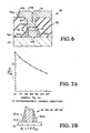
- FIG. 6 shows the result of the contact etch process etching into the tungsten core 10 of an underlying interconnect 16 ⁇ . It is to be noted that penetration of the lower level 16 ⁇ tungsten material 10 only serves to further increase contact interfacial area, which is desirable.
- the aluminum sidewall material may be removed at all contact locations.
- the aluminum will be exposed when etching a contact hole from above (FIG. 6).
- the average spacing which would exist with the clad (cap or encapsulated) prior art tungsten interconnect described above and with the approach of the present invention would be the same, if not slightly greater in the present invention.
- lateral capacitance would be about the same or slightly less.
- the RC time constant, and more particularly, the resistance R would drop in direct relation to the fractional amount of aluminum that can be incorporated into the cross-section, regardless of its arrangement (i.e., sidewalls vs. cap vs. encapsulation), assuming the total cross-sectional area is held constant.
- the maximum fractional amount of aluminum which is usable is determined by how narrow the core 10 can be fabricated and by at what point aluminum, or spacer material 32a, begins to contribute to the makeup of the contact interfaces. Obviously, some aluminum in the contacts is tolerable. The option not to have any is available.
- the freedom to allow the contact hole 20 to be larger than normal and fall off the underlying metal 16 ⁇ and be par tially exposed from above after the overlying interconnect 18 ⁇ is patterned permits the reduction/elimination of dogboning.
- the CVD tungsten plug material 10 of an upper level 18 ⁇ would refill any holes caused by exposure to etch of the core material 10 or sidewall material 32a of the underlying interconnect 16 ⁇ during the etching of the intermetal via contacts 20. If the etching of the core 10 of the upper metal 18 ⁇ is such that the entire contact 20 is not covered by material 10 of 18 ⁇ , then the edges of the core 10b of metal 18 ⁇ will lay over contact 20. So long as sufficient core material 10 remains in the hole 20 to be electrically satisfactory, there is no manufacturability problem.
- FIG. 7a An analysis of resistance reduction with varying areal fractions of aluminum in the interconnect line cross-section, based on the reasonable assumption of parallel electrical resistances shown in FIG. 5b is plotted in FIG. 7a.
- an increase in the amount of aluminum produces a substantial decrease in the resistance of the tungsten/aluminum interconnect trace.
- FIG. 7b depicts the cross-sectional model employed in the analysis, wherein the sidewall portions 32a are assumed to be triangular for the simplicity of an approximate calculation. It is to be noted that in reality, the triangular section underestimates reality, making the graph of FIG. 7a a conservative estimate.
- the process for forming the contact scheme of the invention requires no sloped oxide etching, due to the inherent ability of CVD tungsten to fill cylindrical vias with 100% step coverage. Thus, area is conserved and density can be increased.
- An anisotropic tungsten etch is employed to form the tungsten lines 10.
- Such an etch may comprise CF4 + ⁇ 10% O2 or SF6 + He.
- Many fluorinated gases will etch tungsten satisfactorily.
- the etching is carried out in a plasma (RIE mode) at low pressure and medium power or at higher pressure and higher power in a plasma mode.
- Aluminum 32 is removed from the top 10a of the tungsten lines 10 and from between the lines on the oxide surface 22 by a resistless blanket RIE employing either Cl2 + BCl3, which forms little polymer, or SiCl4 + CHCl3 + Cl2, which forms some sidewall polymer.
- the plasma RIE mode at low pressure and high power gives the best results.
- the former etchant should be run in a sputtering mode to help clean up residual copper from the aluminum.
- the latter etchant results in the formation of polymer and is anisotropic.
- the degree of anisotropy determines how much of metal 32 originally deposited on the sidewalls 10b remains to form the cladding 32a.
- a highly anisotropic etch combined with a conformally coated layer of metal 32 results in the greatest degree of linewidth and overall resistivity control. This is because the sidewall cladding is not attacked by the etch.
- Passivation is performed in CF4 or CHF3 plasma at high pressure and low power.
- Oxide etching to form contact holes 20 is done by RIE or plasma etching, using CHF3 + O2 or CHF3 + C2F6 + He at low or high pressure and medium to high power.
- tungsten etching is done either by RIE, using CF4 + O2 at low pressure and medium power, or by wet etching in a mildly basic solution.
- the tungsten etch should be one that is selective to SiO2 or one that etches SiO2 anisotropically.
- Any aluminum 32a clean-up is done by using the aluminum etch described above.
- a combined etch which attacks both the aluminum and tungsten is also an option.
- the objective is, however, to end up with contact interfaces consisting mainly of tungsten.
Landscapes
- Internal Circuitry In Semiconductor Integrated Circuit Devices (AREA)
- Coupling Device And Connection With Printed Circuit (AREA)
- Compositions Of Oxide Ceramics (AREA)
Priority Applications (1)
| Application Number | Priority Date | Filing Date | Title |
|---|---|---|---|
| AT88301827T ATE83581T1 (de) | 1987-03-10 | 1988-03-02 | Verbindungssystem hoher geschwindigkeit mit feuerfesten kontakten vom ''non-dogbone-typ'' und ein aktiver elektromigrationsunterdrueckender mechanismus. |
Applications Claiming Priority (2)
| Application Number | Priority Date | Filing Date | Title |
|---|---|---|---|
| US07/024,283 US4847674A (en) | 1987-03-10 | 1987-03-10 | High speed interconnect system with refractory non-dogbone contacts and an active electromigration suppression mechanism |
| US24283 | 1987-03-10 |
Publications (3)
| Publication Number | Publication Date |
|---|---|
| EP0282226A2 true EP0282226A2 (de) | 1988-09-14 |
| EP0282226A3 EP0282226A3 (en) | 1989-08-09 |
| EP0282226B1 EP0282226B1 (de) | 1992-12-16 |
Family
ID=21819799
Family Applications (1)
| Application Number | Title | Priority Date | Filing Date |
|---|---|---|---|
| EP88301827A Expired - Lifetime EP0282226B1 (de) | 1987-03-10 | 1988-03-02 | Verbindungssystem hoher Geschwindigkeit mit feuerfesten Kontakten vom "non-dogbone-Typ" und ein aktiver elektromigrationsunterdrückender Mechanismus |
Country Status (5)
| Country | Link |
|---|---|
| US (1) | US4847674A (de) |
| EP (1) | EP0282226B1 (de) |
| JP (1) | JPS63234549A (de) |
| AT (1) | ATE83581T1 (de) |
| DE (1) | DE3876655T2 (de) |
Cited By (1)
| Publication number | Priority date | Publication date | Assignee | Title |
|---|---|---|---|---|
| WO1994009511A1 (en) * | 1992-10-09 | 1994-04-28 | Elsa Elektroniska Systems And Applications Ab | Semiconductor component |
Families Citing this family (89)
| Publication number | Priority date | Publication date | Assignee | Title |
|---|---|---|---|---|
| JP2769331B2 (ja) * | 1988-09-12 | 1998-06-25 | 株式会社日立製作所 | 半導体集積回路の製造方法 |
| JPH04242938A (ja) * | 1991-01-08 | 1992-08-31 | Mitsubishi Electric Corp | 半導体装置およびその製造方法 |
| US5639690A (en) * | 1991-03-12 | 1997-06-17 | Oki Electric Industry Co., Ltd. | Method for manufacturing a conductive pattern structure for a semiconductor device |
| JPH0669208A (ja) * | 1991-03-12 | 1994-03-11 | Oki Electric Ind Co Ltd | 半導体装置 |
| JP3309717B2 (ja) * | 1996-06-26 | 2002-07-29 | 三菱電機株式会社 | 集積回路の配線の製造方法 |
| US20040222525A1 (en) * | 1997-03-14 | 2004-11-11 | Rhodes Howard E. | Advanced VLSI metallization |
| US6242346B1 (en) * | 1997-08-13 | 2001-06-05 | United Microelectronics Corporation | Metallization for uncovered contacts and vias |
| US6653193B2 (en) | 2000-12-08 | 2003-11-25 | Micron Technology, Inc. | Resistance variable device |
| US6457814B1 (en) * | 2000-12-20 | 2002-10-01 | Hewlett-Packard Company | Fluid-jet printhead and method of fabricating a fluid-jet printhead |
| US6638820B2 (en) * | 2001-02-08 | 2003-10-28 | Micron Technology, Inc. | Method of forming chalcogenide comprising devices, method of precluding diffusion of a metal into adjacent chalcogenide material, and chalcogenide comprising devices |
| US6727192B2 (en) | 2001-03-01 | 2004-04-27 | Micron Technology, Inc. | Methods of metal doping a chalcogenide material |
| US6818481B2 (en) | 2001-03-07 | 2004-11-16 | Micron Technology, Inc. | Method to manufacture a buried electrode PCRAM cell |
| US6734455B2 (en) | 2001-03-15 | 2004-05-11 | Micron Technology, Inc. | Agglomeration elimination for metal sputter deposition of chalcogenides |
| US7102150B2 (en) | 2001-05-11 | 2006-09-05 | Harshfield Steven T | PCRAM memory cell and method of making same |
| US6951805B2 (en) | 2001-08-01 | 2005-10-04 | Micron Technology, Inc. | Method of forming integrated circuitry, method of forming memory circuitry, and method of forming random access memory circuitry |
| US6737312B2 (en) | 2001-08-27 | 2004-05-18 | Micron Technology, Inc. | Method of fabricating dual PCRAM cells sharing a common electrode |
| US6784018B2 (en) | 2001-08-29 | 2004-08-31 | Micron Technology, Inc. | Method of forming chalcogenide comprising devices and method of forming a programmable memory cell of memory circuitry |
| US6881623B2 (en) | 2001-08-29 | 2005-04-19 | Micron Technology, Inc. | Method of forming chalcogenide comprising devices, method of forming a programmable memory cell of memory circuitry, and a chalcogenide comprising device |
| US6955940B2 (en) | 2001-08-29 | 2005-10-18 | Micron Technology, Inc. | Method of forming chalcogenide comprising devices |
| US6709958B2 (en) | 2001-08-30 | 2004-03-23 | Micron Technology, Inc. | Integrated circuit device and fabrication using metal-doped chalcogenide materials |
| US6646902B2 (en) | 2001-08-30 | 2003-11-11 | Micron Technology, Inc. | Method of retaining memory state in a programmable conductor RAM |
| US6815818B2 (en) | 2001-11-19 | 2004-11-09 | Micron Technology, Inc. | Electrode structure for use in an integrated circuit |
| US6791859B2 (en) | 2001-11-20 | 2004-09-14 | Micron Technology, Inc. | Complementary bit PCRAM sense amplifier and method of operation |
| US6873538B2 (en) * | 2001-12-20 | 2005-03-29 | Micron Technology, Inc. | Programmable conductor random access memory and a method for writing thereto |
| US6909656B2 (en) | 2002-01-04 | 2005-06-21 | Micron Technology, Inc. | PCRAM rewrite prevention |
| US20030143782A1 (en) * | 2002-01-31 | 2003-07-31 | Gilton Terry L. | Methods of forming germanium selenide comprising devices and methods of forming silver selenide comprising structures |
| US6867064B2 (en) | 2002-02-15 | 2005-03-15 | Micron Technology, Inc. | Method to alter chalcogenide glass for improved switching characteristics |
| US6791885B2 (en) | 2002-02-19 | 2004-09-14 | Micron Technology, Inc. | Programmable conductor random access memory and method for sensing same |
| US7087919B2 (en) | 2002-02-20 | 2006-08-08 | Micron Technology, Inc. | Layered resistance variable memory device and method of fabrication |
| US6847535B2 (en) | 2002-02-20 | 2005-01-25 | Micron Technology, Inc. | Removable programmable conductor memory card and associated read/write device and method of operation |
| US7151273B2 (en) * | 2002-02-20 | 2006-12-19 | Micron Technology, Inc. | Silver-selenide/chalcogenide glass stack for resistance variable memory |
| US6891749B2 (en) * | 2002-02-20 | 2005-05-10 | Micron Technology, Inc. | Resistance variable ‘on ’ memory |
| US6809362B2 (en) | 2002-02-20 | 2004-10-26 | Micron Technology, Inc. | Multiple data state memory cell |
| US6937528B2 (en) | 2002-03-05 | 2005-08-30 | Micron Technology, Inc. | Variable resistance memory and method for sensing same |
| US6849868B2 (en) | 2002-03-14 | 2005-02-01 | Micron Technology, Inc. | Methods and apparatus for resistance variable material cells |
| US6751114B2 (en) * | 2002-03-28 | 2004-06-15 | Micron Technology, Inc. | Method for programming a memory cell |
| US6653236B2 (en) * | 2002-03-29 | 2003-11-25 | Micron Technology, Inc. | Methods of forming metal-containing films over surfaces of semiconductor substrates; and semiconductor constructions |
| US7341947B2 (en) * | 2002-03-29 | 2008-03-11 | Micron Technology, Inc. | Methods of forming metal-containing films over surfaces of semiconductor substrates |
| US6855975B2 (en) | 2002-04-10 | 2005-02-15 | Micron Technology, Inc. | Thin film diode integrated with chalcogenide memory cell |
| US6858482B2 (en) | 2002-04-10 | 2005-02-22 | Micron Technology, Inc. | Method of manufacture of programmable switching circuits and memory cells employing a glass layer |
| US6864500B2 (en) | 2002-04-10 | 2005-03-08 | Micron Technology, Inc. | Programmable conductor memory cell structure |
| US6731528B2 (en) * | 2002-05-03 | 2004-05-04 | Micron Technology, Inc. | Dual write cycle programmable conductor memory system and method of operation |
| US6890790B2 (en) | 2002-06-06 | 2005-05-10 | Micron Technology, Inc. | Co-sputter deposition of metal-doped chalcogenides |
| US6825135B2 (en) | 2002-06-06 | 2004-11-30 | Micron Technology, Inc. | Elimination of dendrite formation during metal/chalcogenide glass deposition |
| US7015494B2 (en) * | 2002-07-10 | 2006-03-21 | Micron Technology, Inc. | Assemblies displaying differential negative resistance |
| US7209378B2 (en) | 2002-08-08 | 2007-04-24 | Micron Technology, Inc. | Columnar 1T-N memory cell structure |
| US7018863B2 (en) | 2002-08-22 | 2006-03-28 | Micron Technology, Inc. | Method of manufacture of a resistance variable memory cell |
| US7163837B2 (en) | 2002-08-29 | 2007-01-16 | Micron Technology, Inc. | Method of forming a resistance variable memory element |
| US20040040837A1 (en) * | 2002-08-29 | 2004-03-04 | Mcteer Allen | Method of forming chalcogenide sputter target |
| US7294527B2 (en) | 2002-08-29 | 2007-11-13 | Micron Technology Inc. | Method of forming a memory cell |
| US7364644B2 (en) | 2002-08-29 | 2008-04-29 | Micron Technology, Inc. | Silver selenide film stoichiometry and morphology control in sputter deposition |
| US6864521B2 (en) | 2002-08-29 | 2005-03-08 | Micron Technology, Inc. | Method to control silver concentration in a resistance variable memory element |
| US6867114B2 (en) | 2002-08-29 | 2005-03-15 | Micron Technology Inc. | Methods to form a memory cell with metal-rich metal chalcogenide |
| US7010644B2 (en) | 2002-08-29 | 2006-03-07 | Micron Technology, Inc. | Software refreshed memory device and method |
| US6867996B2 (en) * | 2002-08-29 | 2005-03-15 | Micron Technology, Inc. | Single-polarity programmable resistance-variable memory element |
| US6831019B1 (en) | 2002-08-29 | 2004-12-14 | Micron Technology, Inc. | Plasma etching methods and methods of forming memory devices comprising a chalcogenide comprising layer received operably proximate conductive electrodes |
| US6813178B2 (en) * | 2003-03-12 | 2004-11-02 | Micron Technology, Inc. | Chalcogenide glass constant current device, and its method of fabrication and operation |
| US7022579B2 (en) * | 2003-03-14 | 2006-04-04 | Micron Technology, Inc. | Method for filling via with metal |
| US7050327B2 (en) | 2003-04-10 | 2006-05-23 | Micron Technology, Inc. | Differential negative resistance memory |
| US6930909B2 (en) | 2003-06-25 | 2005-08-16 | Micron Technology, Inc. | Memory device and methods of controlling resistance variation and resistance profile drift |
| US6961277B2 (en) | 2003-07-08 | 2005-11-01 | Micron Technology, Inc. | Method of refreshing a PCRAM memory device |
| US7061004B2 (en) | 2003-07-21 | 2006-06-13 | Micron Technology, Inc. | Resistance variable memory elements and methods of formation |
| US6903361B2 (en) | 2003-09-17 | 2005-06-07 | Micron Technology, Inc. | Non-volatile memory structure |
| US7583551B2 (en) | 2004-03-10 | 2009-09-01 | Micron Technology, Inc. | Power management control and controlling memory refresh operations |
| US7098068B2 (en) | 2004-03-10 | 2006-08-29 | Micron Technology, Inc. | Method of forming a chalcogenide material containing device |
| US20050274480A1 (en) * | 2004-05-24 | 2005-12-15 | Barsoum Michel W | Reduction of spontaneous metal whisker formation |
| US7354793B2 (en) | 2004-08-12 | 2008-04-08 | Micron Technology, Inc. | Method of forming a PCRAM device incorporating a resistance-variable chalocogenide element |
| US7190048B2 (en) | 2004-07-19 | 2007-03-13 | Micron Technology, Inc. | Resistance variable memory device and method of fabrication |
| US7326950B2 (en) | 2004-07-19 | 2008-02-05 | Micron Technology, Inc. | Memory device with switching glass layer |
| US7365411B2 (en) | 2004-08-12 | 2008-04-29 | Micron Technology, Inc. | Resistance variable memory with temperature tolerant materials |
| US7151688B2 (en) | 2004-09-01 | 2006-12-19 | Micron Technology, Inc. | Sensing of resistance variable memory devices |
| US20060131555A1 (en) * | 2004-12-22 | 2006-06-22 | Micron Technology, Inc. | Resistance variable devices with controllable channels |
| US7374174B2 (en) | 2004-12-22 | 2008-05-20 | Micron Technology, Inc. | Small electrode for resistance variable devices |
| US7317200B2 (en) | 2005-02-23 | 2008-01-08 | Micron Technology, Inc. | SnSe-based limited reprogrammable cell |
| US7709289B2 (en) | 2005-04-22 | 2010-05-04 | Micron Technology, Inc. | Memory elements having patterned electrodes and method of forming the same |
| US7269044B2 (en) | 2005-04-22 | 2007-09-11 | Micron Technology, Inc. | Method and apparatus for accessing a memory array |
| US7427770B2 (en) | 2005-04-22 | 2008-09-23 | Micron Technology, Inc. | Memory array for increased bit density |
| US7269079B2 (en) | 2005-05-16 | 2007-09-11 | Micron Technology, Inc. | Power circuits for reducing a number of power supply voltage taps required for sensing a resistive memory |
| US7233520B2 (en) | 2005-07-08 | 2007-06-19 | Micron Technology, Inc. | Process for erasing chalcogenide variable resistance memory bits |
| US7274034B2 (en) | 2005-08-01 | 2007-09-25 | Micron Technology, Inc. | Resistance variable memory device with sputtered metal-chalcogenide region and method of fabrication |
| US7332735B2 (en) | 2005-08-02 | 2008-02-19 | Micron Technology, Inc. | Phase change memory cell and method of formation |
| US7317567B2 (en) | 2005-08-02 | 2008-01-08 | Micron Technology, Inc. | Method and apparatus for providing color changing thin film material |
| US7579615B2 (en) | 2005-08-09 | 2009-08-25 | Micron Technology, Inc. | Access transistor for memory device |
| US7304368B2 (en) | 2005-08-11 | 2007-12-04 | Micron Technology, Inc. | Chalcogenide-based electrokinetic memory element and method of forming the same |
| US7251154B2 (en) | 2005-08-15 | 2007-07-31 | Micron Technology, Inc. | Method and apparatus providing a cross-point memory array using a variable resistance memory cell and capacitance |
| US7277313B2 (en) | 2005-08-31 | 2007-10-02 | Micron Technology, Inc. | Resistance variable memory element with threshold device and method of forming the same |
| US7560723B2 (en) | 2006-08-29 | 2009-07-14 | Micron Technology, Inc. | Enhanced memory density resistance variable memory cells, arrays, devices and systems including the same, and methods of fabrication |
| US20090102023A1 (en) * | 2007-10-19 | 2009-04-23 | Stephan Wege | Method for Manufacturing a Structure, Semiconductor Device and Structure on a Substrate |
| US8467236B2 (en) | 2008-08-01 | 2013-06-18 | Boise State University | Continuously variable resistor |
Family Cites Families (13)
| Publication number | Priority date | Publication date | Assignee | Title |
|---|---|---|---|---|
| US2922092A (en) * | 1957-05-09 | 1960-01-19 | Westinghouse Electric Corp | Base contact members for semiconductor devices |
| US3838204A (en) * | 1966-03-30 | 1974-09-24 | Ibm | Multilayer circuits |
| US3436615A (en) * | 1967-08-09 | 1969-04-01 | Fairchild Camera Instr Co | Contact metal system of an allayer adjacent to semi-conductor and a layer of au-al intermetallics adjacent to the conductive metal |
| US3647935A (en) * | 1969-12-15 | 1972-03-07 | Motorola Inc | Intermetallic passivation of aluminum metallization |
| JPS5414159A (en) * | 1977-07-05 | 1979-02-02 | Fujitsu Ltd | Manufacture for semiconductor device |
| US4494136A (en) * | 1979-10-04 | 1985-01-15 | Wisconsin Alumni Research Foundation | Semiconductor device having an amorphous metal layer contact |
| US4367119A (en) * | 1980-08-18 | 1983-01-04 | International Business Machines Corporation | Planar multi-level metal process with built-in etch stop |
| US4654680A (en) * | 1980-09-24 | 1987-03-31 | Semiconductor Energy Laboratory Co., Ltd. | Sidewall gate IGFET |
| US4700215A (en) * | 1981-11-19 | 1987-10-13 | Texas Instruments Incorporated | Polycide electrodes for integrated circuits |
| US4712125A (en) * | 1982-08-06 | 1987-12-08 | International Business Machines Corporation | Structure for contacting a narrow width PN junction region |
| US4489482A (en) * | 1983-06-06 | 1984-12-25 | Fairchild Camera & Instrument Corp. | Impregnation of aluminum interconnects with copper |
| US4689113A (en) * | 1986-03-21 | 1987-08-25 | International Business Machines Corporation | Process for forming planar chip-level wiring |
| US4689869A (en) * | 1986-04-07 | 1987-09-01 | International Business Machines Corporation | Fabrication of insulated gate gallium arsenide FET with self-aligned source/drain and submicron channel length |
-
1987
- 1987-03-10 US US07/024,283 patent/US4847674A/en not_active Expired - Lifetime
-
1988
- 1988-03-02 DE DE8888301827T patent/DE3876655T2/de not_active Expired - Lifetime
- 1988-03-02 AT AT88301827T patent/ATE83581T1/de active
- 1988-03-02 EP EP88301827A patent/EP0282226B1/de not_active Expired - Lifetime
- 1988-03-09 JP JP63055950A patent/JPS63234549A/ja active Granted
Cited By (2)
| Publication number | Priority date | Publication date | Assignee | Title |
|---|---|---|---|---|
| WO1994009511A1 (en) * | 1992-10-09 | 1994-04-28 | Elsa Elektroniska Systems And Applications Ab | Semiconductor component |
| US5625207A (en) * | 1992-10-09 | 1997-04-29 | Elsa Elektroniska Systems And Applications Ab | Semiconductor component with conductors at different levels |
Also Published As
| Publication number | Publication date |
|---|---|
| EP0282226A3 (en) | 1989-08-09 |
| ATE83581T1 (de) | 1993-01-15 |
| DE3876655D1 (de) | 1993-01-28 |
| JPS63234549A (ja) | 1988-09-29 |
| DE3876655T2 (de) | 1993-07-01 |
| EP0282226B1 (de) | 1992-12-16 |
| US4847674A (en) | 1989-07-11 |
| JPH0572099B2 (de) | 1993-10-08 |
Similar Documents
| Publication | Publication Date | Title |
|---|---|---|
| EP0282226B1 (de) | Verbindungssystem hoher Geschwindigkeit mit feuerfesten Kontakten vom "non-dogbone-Typ" und ein aktiver elektromigrationsunterdrückender Mechanismus | |
| US4962060A (en) | Making a high speed interconnect system with refractory non-dogbone contacts and an active electromigration suppression mechanism | |
| US6445073B1 (en) | Damascene metallization process and structure | |
| JP2860258B2 (ja) | 相互接続配線の形成方法 | |
| KR100215847B1 (ko) | 반도체 장치의 금속 배선 및 그의 형성 방법 | |
| US6372635B1 (en) | Method for making a slot via filled dual damascene low k interconnect structure without middle stop layer | |
| JP2000208616A (ja) | 半導体装置の製造方法 | |
| US6624514B2 (en) | Semiconductor device and manufacturing method thereof | |
| US6015751A (en) | Self-aligned connection to underlayer metal lines through unlanded via holes | |
| KR100506943B1 (ko) | 식각정지막으로 연결홀의 저측면에 경사를 갖는 반도체소자의 제조 방법들 | |
| US6413863B1 (en) | Method to resolve the passivation surface roughness during formation of the AlCu pad for the copper process | |
| JP3798908B2 (ja) | 半導体装置およびその製造方法 | |
| US7932187B2 (en) | Method for fabricating a semiconductor device | |
| KR0169713B1 (ko) | 집적회로에서 적층 배열된 배선 레벨에 포함된 소자간 결선들 사이에 콘택을 자기정렬방식으로 제조하는 방법 | |
| US6232215B1 (en) | Method for forming increased density for interconnection metallization | |
| JP3525788B2 (ja) | 半導体装置の製造方法 | |
| US6429116B1 (en) | Method of fabricating a slot dual damascene structure without middle stop layer | |
| JP2001176965A (ja) | 半導体装置及びその製造方法 | |
| US6365505B1 (en) | Method of making a slot via filled dual damascene structure with middle stop layer | |
| US6444573B1 (en) | Method of making a slot via filled dual damascene structure with a middle stop layer | |
| KR100578223B1 (ko) | 반도체소자의 듀얼대머신 형성방법 | |
| KR100226786B1 (ko) | 반도체소자의 배선 형성방법 | |
| KR100325303B1 (ko) | 반도체 소자의 금속 배선 및 그의 제조 방법 | |
| KR100312031B1 (ko) | 반도체소자제조방법 | |
| KR100458588B1 (ko) | 반도체 소자 제조 방법 |
Legal Events
| Date | Code | Title | Description |
|---|---|---|---|
| PUAI | Public reference made under article 153(3) epc to a published international application that has entered the european phase |
Free format text: ORIGINAL CODE: 0009012 |
|
| AK | Designated contracting states |
Kind code of ref document: A2 Designated state(s): AT BE CH DE ES FR GB GR IT LI LU NL SE |
|
| PUAL | Search report despatched |
Free format text: ORIGINAL CODE: 0009013 |
|
| AK | Designated contracting states |
Kind code of ref document: A3 Designated state(s): AT BE CH DE ES FR GB GR IT LI LU NL SE |
|
| 17P | Request for examination filed |
Effective date: 19900206 |
|
| 17Q | First examination report despatched |
Effective date: 19910724 |
|
| GRAA | (expected) grant |
Free format text: ORIGINAL CODE: 0009210 |
|
| AK | Designated contracting states |
Kind code of ref document: B1 Designated state(s): AT BE CH DE ES FR GB GR IT LI LU NL SE |
|
| PG25 | Lapsed in a contracting state [announced via postgrant information from national office to epo] |
Ref country code: NL Effective date: 19921216 Ref country code: LI Effective date: 19921216 Ref country code: GR Free format text: LAPSE BECAUSE OF FAILURE TO SUBMIT A TRANSLATION OF THE DESCRIPTION OR TO PAY THE FEE WITHIN THE PRESCRIBED TIME-LIMIT Effective date: 19921216 Ref country code: ES Free format text: THE PATENT HAS BEEN ANNULLED BY A DECISION OF A NATIONAL AUTHORITY Effective date: 19921216 Ref country code: CH Effective date: 19921216 Ref country code: BE Effective date: 19921216 Ref country code: AT Effective date: 19921216 |
|
| REF | Corresponds to: |
Ref document number: 83581 Country of ref document: AT Date of ref document: 19930115 Kind code of ref document: T |
|
| ITF | It: translation for a ep patent filed | ||
| REF | Corresponds to: |
Ref document number: 3876655 Country of ref document: DE Date of ref document: 19930128 |
|
| ET | Fr: translation filed | ||
| PG25 | Lapsed in a contracting state [announced via postgrant information from national office to epo] |
Ref country code: LU Free format text: LAPSE BECAUSE OF NON-PAYMENT OF DUE FEES Effective date: 19930331 |
|
| REG | Reference to a national code |
Ref country code: CH Ref legal event code: PL |
|
| NLV1 | Nl: lapsed or annulled due to failure to fulfill the requirements of art. 29p and 29m of the patents act | ||
| PLBE | No opposition filed within time limit |
Free format text: ORIGINAL CODE: 0009261 |
|
| STAA | Information on the status of an ep patent application or granted ep patent |
Free format text: STATUS: NO OPPOSITION FILED WITHIN TIME LIMIT |
|
| 26N | No opposition filed | ||
| EAL | Se: european patent in force in sweden |
Ref document number: 88301827.7 |
|
| PGFP | Annual fee paid to national office [announced via postgrant information from national office to epo] |
Ref country code: GB Payment date: 19980209 Year of fee payment: 11 |
|
| PGFP | Annual fee paid to national office [announced via postgrant information from national office to epo] |
Ref country code: SE Payment date: 19980302 Year of fee payment: 11 |
|
| PGFP | Annual fee paid to national office [announced via postgrant information from national office to epo] |
Ref country code: FR Payment date: 19980303 Year of fee payment: 11 |
|
| PG25 | Lapsed in a contracting state [announced via postgrant information from national office to epo] |
Ref country code: GB Free format text: LAPSE BECAUSE OF NON-PAYMENT OF DUE FEES Effective date: 19990302 |
|
| PG25 | Lapsed in a contracting state [announced via postgrant information from national office to epo] |
Ref country code: SE Free format text: LAPSE BECAUSE OF NON-PAYMENT OF DUE FEES Effective date: 19990303 |
|
| GBPC | Gb: european patent ceased through non-payment of renewal fee |
Effective date: 19990302 |
|
| EUG | Se: european patent has lapsed |
Ref document number: 88301827.7 |
|
| PG25 | Lapsed in a contracting state [announced via postgrant information from national office to epo] |
Ref country code: FR Free format text: LAPSE BECAUSE OF NON-PAYMENT OF DUE FEES Effective date: 19991130 |
|
| EUG | Se: european patent has lapsed |
Ref document number: 88301827.7 |
|
| REG | Reference to a national code |
Ref country code: FR Ref legal event code: ST |
|
| PG25 | Lapsed in a contracting state [announced via postgrant information from national office to epo] |
Ref country code: IT Free format text: LAPSE BECAUSE OF NON-PAYMENT OF DUE FEES;WARNING: LAPSES OF ITALIAN PATENTS WITH EFFECTIVE DATE BEFORE 2007 MAY HAVE OCCURRED AT ANY TIME BEFORE 2007. THE CORRECT EFFECTIVE DATE MAY BE DIFFERENT FROM THE ONE RECORDED. Effective date: 20050302 |
|
| PGFP | Annual fee paid to national office [announced via postgrant information from national office to epo] |
Ref country code: DE Payment date: 20070330 Year of fee payment: 20 |