EP0282228A1 - Massnahmen zur Verbesserung von Sortiermatrizen mit Stufen - Google Patents
Massnahmen zur Verbesserung von Sortiermatrizen mit Stufen Download PDFInfo
- Publication number
- EP0282228A1 EP0282228A1 EP88301842A EP88301842A EP0282228A1 EP 0282228 A1 EP0282228 A1 EP 0282228A1 EP 88301842 A EP88301842 A EP 88301842A EP 88301842 A EP88301842 A EP 88301842A EP 0282228 A1 EP0282228 A1 EP 0282228A1
- Authority
- EP
- European Patent Office
- Prior art keywords
- signal switching
- switching unit
- input
- matrix
- output ports
- Prior art date
- Legal status (The legal status is an assumption and is not a legal conclusion. Google has not performed a legal analysis and makes no representation as to the accuracy of the status listed.)
- Withdrawn
Links
Images




Classifications
-
- G—PHYSICS
- G06—COMPUTING OR CALCULATING; COUNTING
- G06E—OPTICAL COMPUTING DEVICES
- G06E1/00—Devices for processing exclusively digital data
- G06E1/02—Devices for processing exclusively digital data operating upon the order or content of the data handled
Definitions
- the invention relates to pipeline sort matrices and signal switching assemblies incorporating such matrices.
- EBM Exchange-Bypass Modules
- Such EBMs might be formed from Lithium Niobate Directional Couplers, active fibre couplers, mechanically operated fibre switches or a variety of other possibilites.
- Simple N ⁇ N cross points have been described and fabricated for small arrays, up to perhaps 16 ⁇ 16, but the fabrication complexity escalates rapidly as the number of ports, N, increases.
- Such matrices have the attractive property that they are bi-directional and data transparent so that bidirectional communication can be carried on through them with arbitrary and variable bit-rate and data format.
- a new type of switching network has recently been proposed. This involves the use of a pipeline sort matrix of the kind having a plurality of input and output ports, and a number of signal switching units arranged in series between the input and output ports, the input ports being coupled with an upstream signal switching unit and the output ports being coupled with a downstream signal switching unit, whereby the status of each signal switching unit is reset by supplying selection signals to the signal switching units so that after the status of each signal switching unit has been selected, selected input and output ports are coupled together.
- Such matrices are hereinafter referred to as of the kind described.
- pipeline sort matrix is taken to refer to any matrix which is configured to define a sort algorithm in a pipeline or staged format.
- a method of resetting a pipeline sort matrix of the kind described comprises resetting each signal switching unit in turn.
- a signal switching assembly comprises a pipeline sort matrix of the kind described; and control means for controlling operation of the pipeline sort matrix, the control means generating the selection signals which are supplied to each signal switching unit to reset the status of the signal switching unit, the control means being adapted to reset each signal switching unit in turn.
- the matrix will have N input ports and N output ports, the signal switching units being capable of connecting the input and output ports in any configuration.
- the invention is particularly suitable however, to pipeline sort matrices which perform a perfect shuffle sort algorithm.
- some form of reset signal might be injected to each signal switching unit.
- pipeline sort matrices require clock signals to be supplied to each signal switching unit to control the passage of signals in a pipeline manner through the matrix, it is convenient to define the commencement of a reset period for each signal switching unit by suppressing the clock signal normally fed to that unit.
- the supply of signals to the input ports of the matrix is inhibited, the supply being restarted after resetting of the upstream signal switching unit is completed.
- each signal switching unit could be set by an external selection signal, it is preferable if the selection signals are fed to the input ports of each signal switching unit upstream of the signals to be switched.
- the selection signals could be in the form of matrix output port addresses.
- signal switching units comprise EBMs which respond to the address signals to cause subsequent signals to pass straight through the module (bypass) between the first input and output ports and the second input and output ports respectively or to switch (exchange).
- the signal switching assembly or processor to be described includes a pipeline sort matrix formed from a number of groups of exchange/bypass modules (EBMs).
- EBMs exchange/bypass modules
- An example of the logical construction of an EBM is shown in Figure 1 and comprises four AND gates 1-4 whose outputs are coupled to respective inputs of a pair of OR gates 5, 6.
- the EBM has two input ports A, B connected to the AND gates 1, 2; 3,4 respectively and two output ports D, E connected to the OR gates 5, 6 respectively.
- the output ports of the AND gates 1, 3 are connected to the input ports of the OR gate 5 while the output ports of the AND gates 2, 4 are connected to the input ports of the OR gate 6.
- the status of the EBM is set by a control signal C fed to the AND gates 1, 4 and its logical complement C fed to the AND gates 2,3.
- the EBM is set in its bypass state when the control signal C is logical 1 resulting in a signal on the input port A being passed to the output port D and a signal on the input port B being passed to the output port E.
- the control signal C is logical zero
- the EBM is in its exchange state in which the signal on input port A is coupled with the output port E and the signal on input port B is coupled with output port D.
- Figure 2 illustrates a generalised sort processor having N input ports and N output ports.
- the input ports are connected in pairs to respective EBMs of a first group 7 whose output ports are connected to a redistribution network 8.
- the redistribution network has a fixed pattern and couples each input line with a respective output line.
- this generalised sort processor comprises a number of pairs of EBM groups and redistribution networks together with a final group of EBMs 9 connected to the output ports of the processor.
- the redistribution networks should be arranged such that the matrix performs a perfect shuffle algorithm. This is particularly suitable for optical signal implementation since each redistribution network has an identical form and so can be fabricated by a common network.
- logical EBM a module that includes the logic to establish whether it should self set to the exchange or bypass state according to the address data presented to it through its input ports.
- the "0" module always bypasses whilst the "+” and “-” modules always route the larger of the two addresses (numbers) to the port marked "h”. They are thus logically identical in structure but are mirror images in function.
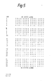
- Figure 5 shows the logical layout for a full 32 ⁇ 32 matrix using the perfect shuffle sort algorithm for its self addressing function.
- the layout has been deliberately split into five groups of five rows, with each row containing 16 modules.
- the data lines emerging from each row of 16 EBMs are perfect shuffled before entering the next row.
- the input data has been sorted into 8 bitonic sequences, with the adjacent pairs of inputs reversed or not according to the address size and spatial position.
- the addresses have been sorted into 4 bitonic sequences, 2, 1 and finally into a linearly ascending sequence at row 25.
- each EBM is determined by address data supplied to each input port of the matrix. This address data defines the matrix output port to which subsequent signals are to be switched.
- the use of logical EBMs is particularly advantageous in this connection since they respond to the relative size of the two addresses arriving at each input port of the respective pair (see Truth Table of Figure 3B). The only action required on the EBM is always to deliver the larger number to the same defined (by position) exit port. Such a logical operation on binary MSB first addresses is trivial, since identical bits always pass directly through. The first pair of bits in the address to differ then define uniquely the larger of the two numbers.
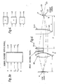
- Figure 3a illustrates the overall logical circuit for an EBM where I1, I2, O1, O2 are the input ports and output ports respectively; R indicates a reset signal; and P, Q indicate control inputs and outputs for latching the EBM in one of its two states.
- the reset signal R will be logical 1 and the signals P, Q will define whether the state is bypass, exchange, or not yet set.
- the reset signal is switched to zero causing Q(n) and P(n) to be zeroed thus implying that the EBM is thereafter not set and preparing the EBM to be set once the reset signal returns to logical 1.
- Figures 6 to 9 illustrate a practical implementation of a perfect shuffle sort matrix of the type shown in Figure 2.
- each redistribution network has an identical form and in this example is defined optically by a lens system 11.
- this shuffle optics relies upon the concept of magnifying an image laterally by a factor of 2, shearing the image into two, and overlaying the two halves to form a shuffled image. It also has some additional advantages not previously achieved since it allows the whole optical system to be folded into a compact sub unit embracing the return data path to the array. It also brings together all the input/output and control channels in a single port 12 located opposite the logic array 10.
- the logic array 10 is fabricated on a single chip of for example GaInAs/InP with a band gap in the 1300-1500 nm region.
- the array comprises a number of MQW electro-absorption modulators (EAM), two for each EBM, each of which can be addressed by an externally generated "read" laser beam.
- EAM MQW electro-absorption modulators
- FIG. 9 An example of one EBM within the logic array is shown in Figure 9.
- This comprises a pair of photodetectors 13,14 formed, for example, from electro-absorbtion modulators.
- the electronic output signals from these photodetectors 13, 14 are fed to respective gain and thresholding circuits 15 whose outputs are fed to an EBM logic circuit 16.
- a photodetector 17 also formed from an electro-absorbtion modulator is responsive to a clock laser beam to provide clock signals to the EBM logic circuit 16.
- the electronic output signals from the EBM logic circuit 16 are fed to respective EAM drivers 18, 19 which drive respective electro-absorption modulators 20, 21.
- An external read beam is supplied to each EAM 20, 21 which modulates the beam to generate the required output signal.
- the optical source of the "read" beam can be located away from the active chip and can thus dissipate its heat elsewhere. This has a secondary, but important advantage, that this enables the beam also to be used for timing and control purposes.
- the exit beam direction can be derived from the input. This is highly desirable in order to implement the shuffle wiring scheme.
- EAMs are known to be inherently fast (sub 100 ps switching speed), are readily fabricated and lend themselves to monolithic integration. They are also (optically) non-resonant so that they are relatively insensitive to temperature and wavelength.
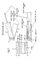
- the input/output system positioned at the port 12 in Figure 6 is illustrated in detail in Figure 7.
- a composite, layered I/O structure 22 shown in detail in Figure 7A This comprises the output end of an input fibre array 23 composed of a number of optical fibres, one for each input port of the matrix, as a top layer followed by alternate layers of microlenses 24 and reflectors 25, there being one pair of layers 24, 25 corresponding to each row of EBMs, and terminating with the input end 26 of an output fibre array 27.
- each EBM In order for the EBMs to function, it is necessary to supply three pump laser beams to each EBM. These provide the two "read" beams to the EAMs 20, 21 and the clock beam supplied to the photodetector 17.
- Each set of three beams is provided in this example by a respective laser the power from which is fanned out into 3 N/2 spots (N is the number of EBMs) on the associated row position on the I/O element 22 to generate three beams to each EBM.
- These beams are fed via the microlenses 24 associated with the respective EBM row to the logic array 10.
- Each laser thus provides synchronisation and interrogation for all the EBMs in a single logical row of the pipeline. The laser will be clocked with the appropriate phaseing for that row position. Since all the M(M-1)+1 clock lasers can be colocated in a linear array and will require identical delays between each, it is believed that very accurate clocking should be possible. In addition, the rows enjoy zero clock skew as a result of the
- interrogation beams from the pump source previously described are injected via the first row of microlenses 24, the interrogation beams impinging onto the logic array at different angles which will be imposed upon them by means of prisms (solid or holographic) located at the I/O element 22.
- the prisms are indicated by reference numeral 30 ( Figure 6). The reason for this is that it is desirable to spatially separate the optical beams emerging from the two halves (1 to P and P+1 to N) of the array in order to operate the shuffle optical system with minimum power loss.
- the two read beams are reflected from the respective EAMs 20, 21 after modulation and are guided by the shuffle optics 11 to impinge upon the first reflector layer 25 of the I/O element 22 to form a shuffled array of outputs at the reflector and are then imaged back to the input photodetector array of the next row of EBMs.
- This sequence is then repeated for each row of EBMs with the read beams from the final row of EAMs being guided to the output fibre array 26.
- Figure 8 shows a block diagram of the complete processor.
- a storage register, 33 is positioned which notionally uses electronic logic.
- N registers store the desired matrix output port address associated with each matrix input port. Thus if input port 23 is to be connected to output port 56, the number 56 is stored in the 23rd address register.
- the address register 33 the complete set of addresses from 1 to N is stored. If some channels are not active, then one of the unused exit port addresses is stored in its register.
- An input buffer 32 is set in the data input line to store data during the reset intervals. This need not be very large, perhaps 20 to 30 bits per input line.
- the processor is controlled by timing electronics 34.
- the clock signal (CK) generated by a clock laser array 36 as previously described is removed (turn off the appropriate clock laser) and the EBM logic is designed so that it falls back to the reset state in the absence of the clock. Any row of the matrix can now be reset at will.
- the set of N output port addresses is injected via a fibre laser input array 35 and the data path 23 in MSB first format.
- the EBM examines addresses entering its input ports and as soon as two address bits differ, latches to the appropriate exchange or bypass state and remains there until reset. Immediately following the address bits (7 bits), the data from the buffer 32 follows. If no data is present on a line, then we may consider that channel as remaining idle. In practice it might be necessary to inject some dummy data to limit the signal disparity in the electronic EBM stages.
Landscapes
- Engineering & Computer Science (AREA)
- Theoretical Computer Science (AREA)
- Physics & Mathematics (AREA)
- General Physics & Mathematics (AREA)
- Use Of Switch Circuits For Exchanges And Methods Of Control Of Multiplex Exchanges (AREA)
- Optical Communication System (AREA)
- Investigating Or Analyzing Materials By The Use Of Ultrasonic Waves (AREA)
- Pipeline Systems (AREA)
Applications Claiming Priority (2)
| Application Number | Priority Date | Filing Date | Title |
|---|---|---|---|
| GB8705053 | 1987-03-04 | ||
| GB878705053A GB8705053D0 (en) | 1987-03-04 | 1987-03-04 | Pipeline sort matrices |
Publications (1)
| Publication Number | Publication Date |
|---|---|
| EP0282228A1 true EP0282228A1 (de) | 1988-09-14 |
Family
ID=10613313
Family Applications (1)
| Application Number | Title | Priority Date | Filing Date |
|---|---|---|---|
| EP88301842A Withdrawn EP0282228A1 (de) | 1987-03-04 | 1988-03-02 | Massnahmen zur Verbesserung von Sortiermatrizen mit Stufen |
Country Status (5)
| Country | Link |
|---|---|
| EP (1) | EP0282228A1 (de) |
| JP (1) | JPH02502775A (de) |
| AU (1) | AU1360188A (de) |
| GB (1) | GB8705053D0 (de) |
| WO (1) | WO1988006829A1 (de) |
Cited By (1)
| Publication number | Priority date | Publication date | Assignee | Title |
|---|---|---|---|---|
| GB2311180A (en) * | 1996-03-13 | 1997-09-17 | Northern Telecom Ltd | Switch Architecture |
Families Citing this family (1)
| Publication number | Priority date | Publication date | Assignee | Title |
|---|---|---|---|---|
| GB8904281D0 (en) * | 1989-02-24 | 1989-04-12 | British Telecomm | Optical interconnect networks |
Citations (1)
| Publication number | Priority date | Publication date | Assignee | Title |
|---|---|---|---|---|
| WO1987000314A1 (en) * | 1985-06-24 | 1987-01-15 | American Telephone & Telegraph Company | Optical shuffle arrangement |
-
1987
- 1987-03-04 GB GB878705053A patent/GB8705053D0/en active Pending
-
1988
- 1988-03-02 WO PCT/GB1988/000156 patent/WO1988006829A1/en not_active Ceased
- 1988-03-02 AU AU13601/88A patent/AU1360188A/en not_active Abandoned
- 1988-03-02 EP EP88301842A patent/EP0282228A1/de not_active Withdrawn
- 1988-03-02 JP JP63502040A patent/JPH02502775A/ja active Pending
Patent Citations (1)
| Publication number | Priority date | Publication date | Assignee | Title |
|---|---|---|---|---|
| WO1987000314A1 (en) * | 1985-06-24 | 1987-01-15 | American Telephone & Telegraph Company | Optical shuffle arrangement |
Non-Patent Citations (4)
| Title |
|---|
| IEE PROCEEDINGS, vol. 132, no. 6, part J, December 1985, pages 371-383, Hitchin, GB; J.E. MIDWINTER: "'Light' electronics, myth or reality?" * |
| IEEE TRANSACTIONS ON COMPUTERS, vol. C-20, no. 2, February 1971, pages 153-161, IEEE, New York, US; H.S. STONE: "Parallel processing with the perfect shuffle" * |
| PROCEEDINGS OF THE IEEE, vol. 72, no. 7, July 1984, pages 850-866, IEEE, New York, US; J.W. GOODMAN et al.: "Optical interconnections for VLSI systems" * |
| THE 6TH ANNUAL SYMPOSIUM ON COMPUTER ARCHITECTURE, 23rd-25th April 1979, pages 168-177, IEEE, New York, US; J.H. PATEL: "Processor-memory interconnections for multiprocessors" * |
Cited By (2)
| Publication number | Priority date | Publication date | Assignee | Title |
|---|---|---|---|---|
| GB2311180A (en) * | 1996-03-13 | 1997-09-17 | Northern Telecom Ltd | Switch Architecture |
| GB2311180B (en) * | 1996-03-13 | 2000-03-22 | Northern Telecom Ltd | Switch architecture |
Also Published As
| Publication number | Publication date |
|---|---|
| JPH02502775A (ja) | 1990-08-30 |
| WO1988006829A1 (en) | 1988-09-07 |
| GB8705053D0 (en) | 1987-04-08 |
| AU1360188A (en) | 1988-09-26 |
Similar Documents
| Publication | Publication Date | Title |
|---|---|---|
| US5414819A (en) | Optical interconnection network | |
| Hinton | Photonic switching fabrics | |
| AU618477B2 (en) | Network topology for reduced blocking and photonic system implementation thereof | |
| US5013140A (en) | Optical space switch | |
| US5648859A (en) | Liquid crystal microprism array, free-space optical interconnector, and optical switch | |
| JP2004029811A (ja) | 導波型光クロスポイントスイッチ | |
| EP0435296A1 (de) | Optischer räumlicher Schalter und Netzwerk mit derartigen optischen räumlichen Schaltern | |
| Midwinter | Novel approach to the design of optically activated wideband switching matrices | |
| EP0229177B1 (de) | Optische umordnungsanordnung | |
| EP0397368B1 (de) | Steuerungsverfahren für Raumvielfachkoppelnetz | |
| US5153757A (en) | Network control arrangement | |
| EP0397369B1 (de) | Optische Vorrichtung zum Kombinieren von Lichtstrahlen-Matrizen mit verschiedenen Wellenlängen | |
| Midwinter | Photonics in switching: the next 25 years of optical communicationss? | |
| EP0282227A1 (de) | Signalschaltprozessor | |
| AU1360188A (en) | Improvements relating to pipeline sort matrices | |
| US5172259A (en) | Embedded control network | |
| JPS60254991A (ja) | 時分割光交換機 | |
| US6545792B2 (en) | Polarization independent non-blocking all-optical switching device | |
| CN117170025B (zh) | 一种波长选择开关及光信号处理方法 | |
| JP3023221B2 (ja) | 多端子光スイッチ | |
| Choudhary et al. | Optical switching and routing architectures for fiber-optic computer communication networks | |
| JP2855878B2 (ja) | 光セルフルーティング回路 | |
| KR100245393B1 (ko) | 편광 변조 표면방출 레이저를 이용한 광스위칭 장치 | |
| Lugagne Delpon et al. | Operation of 4× 1 optical register as a fast access optical buffer memory | |
| Midwinter | Photonic switching technology |
Legal Events
| Date | Code | Title | Description |
|---|---|---|---|
| PUAI | Public reference made under article 153(3) epc to a published international application that has entered the european phase |
Free format text: ORIGINAL CODE: 0009012 |
|
| AK | Designated contracting states |
Kind code of ref document: A1 Designated state(s): AT BE CH DE ES FR GB GR IT LI LU NL SE |
|
| 17P | Request for examination filed |
Effective date: 19890218 |
|
| 17Q | First examination report despatched |
Effective date: 19910405 |
|
| STAA | Information on the status of an ep patent application or granted ep patent |
Free format text: STATUS: THE APPLICATION IS DEEMED TO BE WITHDRAWN |
|
| 18D | Application deemed to be withdrawn |
Effective date: 19910819 |