EP0282836A2 - Procédé et appareil pour déposer des couches à haute résistance ohmique par pulvérisation cathodique - Google Patents
Procédé et appareil pour déposer des couches à haute résistance ohmique par pulvérisation cathodique Download PDFInfo
- Publication number
- EP0282836A2 EP0282836A2 EP88103333A EP88103333A EP0282836A2 EP 0282836 A2 EP0282836 A2 EP 0282836A2 EP 88103333 A EP88103333 A EP 88103333A EP 88103333 A EP88103333 A EP 88103333A EP 0282836 A2 EP0282836 A2 EP 0282836A2
- Authority
- EP
- European Patent Office
- Prior art keywords
- target
- substrate
- distance
- shielding device
- reaction gas
- Prior art date
- Legal status (The legal status is an assumption and is not a legal conclusion. Google has not performed a legal analysis and makes no representation as to the accuracy of the status listed.)
- Granted
Links
Images

Classifications
-
- H—ELECTRICITY
- H01—ELECTRIC ELEMENTS
- H01J—ELECTRIC DISCHARGE TUBES OR DISCHARGE LAMPS
- H01J37/00—Discharge tubes with provision for introducing objects or material to be exposed to the discharge, e.g. for the purpose of examination or processing thereof
- H01J37/32—Gas-filled discharge tubes
- H01J37/32431—Constructional details of the reactor
- H01J37/3244—Gas supply means
-
- C—CHEMISTRY; METALLURGY
- C23—COATING METALLIC MATERIAL; COATING MATERIAL WITH METALLIC MATERIAL; CHEMICAL SURFACE TREATMENT; DIFFUSION TREATMENT OF METALLIC MATERIAL; COATING BY VACUUM EVAPORATION, BY SPUTTERING, BY ION IMPLANTATION OR BY CHEMICAL VAPOUR DEPOSITION, IN GENERAL; INHIBITING CORROSION OF METALLIC MATERIAL OR INCRUSTATION IN GENERAL
- C23C—COATING METALLIC MATERIAL; COATING MATERIAL WITH METALLIC MATERIAL; SURFACE TREATMENT OF METALLIC MATERIAL BY DIFFUSION INTO THE SURFACE, BY CHEMICAL CONVERSION OR SUBSTITUTION; COATING BY VACUUM EVAPORATION, BY SPUTTERING, BY ION IMPLANTATION OR BY CHEMICAL VAPOUR DEPOSITION, IN GENERAL
- C23C14/00—Coating by vacuum evaporation, by sputtering or by ion implantation of the coating forming material
- C23C14/22—Coating by vacuum evaporation, by sputtering or by ion implantation of the coating forming material characterised by the process of coating
- C23C14/34—Sputtering
- C23C14/35—Sputtering by application of a magnetic field, e.g. magnetron sputtering
-
- H—ELECTRICITY
- H01—ELECTRIC ELEMENTS
- H01J—ELECTRIC DISCHARGE TUBES OR DISCHARGE LAMPS
- H01J37/00—Discharge tubes with provision for introducing objects or material to be exposed to the discharge, e.g. for the purpose of examination or processing thereof
- H01J37/32—Gas-filled discharge tubes
- H01J37/34—Gas-filled discharge tubes operating with cathodic sputtering
- H01J37/3402—Gas-filled discharge tubes operating with cathodic sputtering using supplementary magnetic fields
- H01J37/3405—Magnetron sputtering
- H01J37/3408—Planar magnetron sputtering
-
- H—ELECTRICITY
- H01—ELECTRIC ELEMENTS
- H01J—ELECTRIC DISCHARGE TUBES OR DISCHARGE LAMPS
- H01J2237/00—Discharge tubes exposing object to beam, e.g. for analysis treatment, etching, imaging
- H01J2237/32—Processing objects by plasma generation
- H01J2237/33—Processing objects by plasma generation characterised by the type of processing
- H01J2237/332—Coating
- H01J2237/3321—CVD [Chemical Vapor Deposition]
Definitions
- the invention relates to a method according to the preamble of patent claim 1.
- High-resistance layers are understood to mean those with specific resistances above 5 ⁇ 10 ⁇ 4 ohm / cm, but this limit value is not critical and should be assessed differently from case to case. Such layers already have the properties of insulator layers on condensation surfaces for the scattered particles.
- the reaction gas can be, for example, a pure reaction gas such as oxygen or nitrogen, or a mixture of at least one of these gases with an inert gas required for the atomization process, such as argon.
- the target In order to be able to operate the atomization process with DC voltage, the target must be electrically conductive; it generally consists of a metal which forms one reaction component for the layer to be produced, while the other reaction component comes from the reaction gas.
- the interaction of metal vapor flow and reaction gas causes the desired compounds to be deposited on the substrate.
- the reaction gas works however, also on the target surface and creates an insulating coating on a more or less large area of the target surface, by means of which the atomization rate is reduced and the stability of the process is impaired.
- only the erosion trench typical of magnetron cathodes, which runs within the tunnel consisting of magnetic field lines, through which the plasma discharge is enclosed, is largely kept free of the insulating covering. At the bottom of the erosion trench, the atomization rate is so high with practically usable process control that no disruptive insulating coating can form.
- a number of other process parameters must be observed here.
- a high level of decoupling between the substrate and the target is generally used.
- the effect of the reaction gas on the substrate is increased relative to the effect on the target due to the area ratio of the substrate area to the effective target area (area of the erosion trench on the target).
- a high level of decoupling is achieved, among other things, by a large distance between the target and the substrate, which is usually about 100 mm.
- Another decoupling measure is the separation of the inlet points of the working gas (eg argon) and reaction gas, the working gas near the target and the Reaction gas (or a mixture of working and reaction gas) is admitted near the substrate.
- a relatively high process stability is achieved if an orifice located between the inlet points of the gases is also introduced, which largely separates the area near the substrate from the area near the target. This aperture acts as an additional getter area for the reaction gas in the area close to the target.
- the introduction of reaction gas into the area near the target is thereby reduced and at the same time the effect of the reaction gas on the substrate is increased.
- the discharge current must be maintained when working with a diaphragm by means of an additional anode which is arranged on the side of the diaphragm facing the substrate (DE-OS 33 31 707).
- the known solutions lead to technical disadvantages.
- the achievable precipitation rates are considerably reduced due to the large target-substrate distance, but in particular because approximately 60% of the atomized target material hits the screen.
- the aperture also noticeably reduces the density of the plasma in the area close to the substrate.
- a larger excess of reaction gases has to be used, which in itself calls for an increase in process stability by Keeping the reaction gas away from the target is diametrically opposite.
- the known solution is particularly unsuitable for ion-assisted coating.
- the known device also tends to malfunctions, since layers grow on the panel, which peel off, especially when it comes to insulating layers.
- the invention is therefore based on the object of specifying a method of the type described in the introduction with which insulating layers or high-resistance layers can be deposited at a high rate with great process stability.
- the transverse dimension "c" is the diameter of the target and the distance "x" corresponds to the inside diameter of the shielding device.
- This coordination can also be readily transferred to rectangular targets, in which the inner edges of the shielding device then run parallel to one another at a distance "x".
- the dimensioning rule mentioned means that at least 60% of the particle stream can flow unhindered in the direction of the substrate.
- the shielding device which also performs an anode function in a certain method, is arranged in the immediate vicinity of the substrate plane. It is particularly advantageous here if the distance "d" between the surface of the shielding device facing the target and the substrate corresponds at most to the sum of the thickness of the shielding device and a gap with a width of 5 mm. This allows the plasma to be practically unhindered and with high density act on the substrate or the layer under construction there.
- the discharge current cannot reach the usually present dark room shield or the plasma shield, but is derived in the vicinity of the substrate.
- the plasma density increases in the area close to the substrate.
- the reaction gas is used more effectively, i.e. Compared to the decoupling procedure, far less reaction gas is required to achieve a certain degree of reaction.
- this type of design of the potential relationships in the area of the shielding device or the anode can surprisingly achieve an increase in the basic stability of the discharge.
- a very decisive advantage in the procedure according to the invention is the gain in long-term constancy of the coating parameters and thus the layer properties.
- insulating layers are deposited on the shielding device or other parts of the device located in the vicinity of the reaction zone. Since the parts mentioned are usually electrically conductive metal parts, this changes Potential distribution in the course of the coating.
- coating material is also condensed on the shielding device in the method according to the invention, the method according to the invention ensures that these influences have no harmful effects on the long-term stability of the process parameters. This means that potential conditions that are defined from the start and optimal for the coating process are achieved.
- suction power of a vacuum pump device determining the negative pressure on the one hand and the amount of reaction gas supplied per unit of time on the other hand are set such that less than 1/3, preferably less than 1/5, of the supplied from the reaction zone between target and substrate Reaction gas is withdrawn unused.
- the ratio of the supplied to the unused amount of reaction gas can be determined in a particularly simple manner by selecting a gap width between an inner housing surrounding the cathode and the substrate. It can thereby be achieved that the difference between the total pressures in said inner housing and in the vacuum chamber surrounding the inner housing is small by a factor of 2.
- reaction gas has to flow almost completely from the inlet point in the vicinity of the target into the region of the dense plasma in front of the target surface and diffuses from there to the substrate, where it is largely consumed in the chemical reaction before a small proportion the column installed there is suctioned off.
- the density of excited reaction gas particles in front of the substrate surface is significantly increased in this way. This in turn has the consequence that the ratio of the number of impulses required to set the required degree of reaction is lower. As a result, a larger amount of metal per unit time can be reacted with a higher degree of reaction with the same or even lower reaction gas flow.
- the discharge can be operated stably when using the method according to the invention, although it would have to be expected that admitting the reaction gas near the target, but in particular the close coupling between the target and the substrate itself, would reduce the basic stability of the discharge.
- the invention also relates to a device for carrying out the method according to the preamble of claim 10.
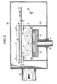
- FIG. 1 shows a magnetron cathode 1 which, taken on its own, belongs to the prior art. Details of the basic design of such a magnetron cathode can also be found in FIG. 3.
- the magnetron cathode 1 is connected via a line 2 to a direct voltage source 3 which is able to deliver a negative direct voltage between approximately 400 and 1000 volts.
- the magnetron cathode 1 is coated with an approximately congruent target 4 made of an electrically conductive material, which supplies the one component of the layer material to be formed.
- the target has a surface 4a, which is the so-called atomizing surface.
- the magnetron cathode or the target 4 is surrounded in the edge region by a distribution device 5 for the reaction gas, the distance being chosen as small as possible, without however the distribution device 5 and the target surface 4a overlap when viewed in plan view.
- the outlet openings of the distribution device 5, which are not designated in any more detail, are directed downward.
- the target 5 has the transverse dimension "c".
- the distribution device 5 is also shown as a ring line, which is not shown in the drawing for the sake of clarity.
- the distance from the target surface 4a to the substrate 6 has the dimension "a". This distance is between 40 and 60 mm, while the transverse dimension "c" of the target is no longer critical and has the usual dimensions.
- Within this distance "a” there is - in closer proximity to the substrate 6 - a shielding device 7, the inner edges 7a of which have a distance "x" from one another which is between 0.6 times and 2.0 times the transverse dimension "c" of the target 4.
- the variability of this distance "x" is symbolized by the dashed extensions of the shielding device 7.
- the shielding device 7 is arranged in isolation, which is indicated by a post insulator 8 shown on the left. It is also connected via a line 9 to a DC voltage source 10, which is able to deliver a DC voltage between 0 and +200 volts.
- the surface 7b of the shielding device facing the target 4 is at a distance "d" from the substrate 6 which is less than half the distance "a". In the exemplary embodiment, the distance “d” is at most the sum of the thickness of the shielding device 7 and the width of a gap 11 of approximately 5 mm.
- FIG. 1 shows an arrangement in which the magnetron cathode 1 is at a relatively large distance from a wall 12 of the vacuum chamber lying to the side of it. The distance is bridged by another wall 13 of the vacuum chamber, which is at ground potential overall.
- the chamber walls 12 and 13 are covered with layers 14 and 15 of at least partially insulating material, as a result of which the chamber walls gradually lose their anode function compared to the initial state.
- part B the magentron cathode is shown in a confined space, i.e. the wall 16 of the vacuum chamber lying at ground potential is very much shorter.
- the immediately adjacent side wall 17 of the vacuum chamber is suspended in isolation, which is indicated by a support insulator 18.
- the wall 17 can adjust itself to a freely chosen intermediate potential.
- the two variants according to Figure 1 are particularly suitable for the deposition of layers with a certain residual conductivity, such as SiO2.
- the parts acting as an anode are either at ground or connected to positive potential against ground and arranged in the direct particle stream in front of the substrate.
- layers condense on the parts acting as the anode which are still sufficiently conductive to absorb the discharge current. Insulating layers can easily be deposited on the other surfaces. If work is carried out with zero potential on the shielding device 7 acting as an anode, it can be short-circuited to the wall 12 (FIG. 2, part A).
- the shielding device 7, which acts as an anode is arranged separately from the surrounding walls, which act as a plasma screen, for example when these walls can "float” like wall 17 because they are suspended in isolation (FIG. 1, part B).
- the two variants A and B according to FIG. 2 correspond essentially in size and arrangement to the corresponding variants A and B according to FIG. 1, so that the same reference numerals have been used.
- the variants according to FIG. 2 are intended for the production of insulating layers.
- an insulating layer 19 also condenses on the shielding device 7, so that this - at least after some time - can no longer perform the function of an anode.
- a special anode 20 is seen behind the shielding device 7 in the atomization direction arranged, which is designed as a water-flow tube.
- the anode 20 is connected via a line 21 to a DC voltage source 22, through which the anode can be supplied with a positive voltage between approximately 40 and 120 volts.
- the anode 20 is set back in the gap 11 with respect to the edges 7a to such an extent that it can only be hit by insulating particles to a very small extent.
- the shielding device 7 is either connected to the ground potential together with the walls 12 and 13 (FIG. 2, part A) or is kept at an automatically adjustable potential by a post insulator 8 (FIG. 2, part B). In any case, the shielding device 7 also has a shielding function with respect to the special anode 20.
- the anode 20 and the shielding device 7 are both arranged in close proximity to the substrate, in such a way that the proportion of the coating material which reaches the substrate 6 is practically not changed by the shielding device 7.
- the potential relationships in the entire plasma space, in particular in the vicinity of the substrate, remain stable in terms of time and space if an insulating layer is formed on the surfaces mentioned or is already present.
- the parts mentioned must be electrically conductive, since otherwise they would not be able to fulfill their tasks in the area of the cathode to suppress disruptive secondary discharges.
- a vacuum chamber 23 is also shown schematically, which has been omitted in FIGS. 1 and 2.
- This vacuum chamber is connected via a suction port 24 to a set of vacuum pumps, not shown.
- An inner housing 25 is arranged within the vacuum chamber 23 and encloses the magnetron cathode 1 and the distribution device 5 as closely as possible.
- the cathode 1 with its target 4 is shown here in somewhat more detail, specifically the magnetic poles N and S are shown, which generate a self-contained field line tunnel over the target surface 4a, in which the plasma P is enclosed.
- the plasma follows the course of the pole faces; in the case of a circular magentron cathode it has the shape of a torus.
- the magnetron cathode 1 also includes a basic cathode body 1a.
- the line 2 is designed here as a support tube and is guided through the wall of the vacuum chamber 23 by means of a bushing insulator 26.
- the side surfaces, the rear side and the line 2 are surrounded by a dark room shield 27 which is also at ground potential.
- the shielding device 7 is part of the inner housing 25 and is at ground potential with this.
- An outlet opening for the coating material which has the dimension “x”, is formed between the inner edges 7a in a manner analogous to that in FIGS. 1 and 2.
- a circumferential gap 11 with a defined width w and a defined length s is formed on the circumference of the inner housing 25. This creates a certain throttling effect, which, however, enables gas exchange through flow and diffusion.
- Either pure reaction gas or reaction gas mixed with a working gas (argon) can be fed through the distribution device 5.
- a further distribution device 28 is arranged outside the inner housing 25, but inside the vacuum chamber 23, through which pure working gas (argon) is supplied, for example.
- a reaction zone R is delimited between the target 4 and the substrate 6 by the inner housing 25 (analogously to the wall 17 in FIGS. 1 and 2), and such a state of equilibrium of the gas movements is achieved through the gap 11 that less than 1 from the reaction zone R / 3, preferably less than 1/5 of the unused reaction gas can be drawn off through the suction port 24.
- the gap 29 on the back of the substrate 6 is less critical. It is supported by a plate 30 limited, which, however, becomes important for the plasma process if the substrate 6 consists, for example, of a sequence of individual plate-shaped substrates which are guided through the reaction zone R at a distance.
- the measures described above ensure that the reaction gas flows almost completely from the distributor 5 in the vicinity of the target into the area of the dense plasma in front of the target surface and diffuses from there to the substrate, where it is mostly in the chemical reaction is consumed. Only the above-mentioned remaining amount is sucked off through the gap 11 present there. In this way, it is prevented that the excited reaction gas is sucked off directly from the vacuum pumps and thus removed from the conversion into chemical compounds on the substrate. In this way, the density of excited reaction gas particles in front of the substrate surface is increased. This in turn has the consequence that the ratio of the shock numbers required for setting the required degree of reaction becomes lower.
- the measures for forming defined flow conditions consist in the selection of defined gap widths and / or gap lengths between the substrate 6 and the inner housing 25 on the one hand and in the selection of an effective suction power of the vacuum pumps on the suction nozzle 24.
- the working gas in addition to the reaction gas, the working gas (argon) is also let into the inner housing 25, or the reaction gas is let into the said case alone.
- the flow rate which is determined by the dimensions of the gap 11, as the sum of the flow rates of reaction gas and working gas at a selected total pressure in the inner housing 25, must be adapted to the effective pumping speed of the vacuum pump by the total pressure in the vacuum chamber 23.
- the working gas is admitted through the distribution device 28 into the vacuum chamber 23 and reaches the inner housing 25 by diffusion, in which the reactive process takes place.
- the gap 11 is essentially only dimensioned for the reaction gas flow which is to be suctioned off.
- both cases have in common that the partial pressure difference between the inner housing 25 and the space in the vacuum chamber 23 is kept small in order to produce only a small reaction gas flow through the gap 11.
- the effective suction power was set to 100 l / s.
- the magnetron cathode had a length of 500 mm and was supplied with a power stabilized power supply with a power of 1000 W.
- the total pressure in the vacuum chamber 23 was 4 ⁇ 10 ⁇ 3 mbar, and the distance "a" between target surface and substrate was 40 mm.
- a flow of 350 sccm of pure oxygen was admitted into the inner housing 25 via the distribution device 5 and a flow of 250 sccm argon via the distribution device 28.
- the pressure difference achieved on both sides of the gap 11 was 1.7 ⁇ 10 -3 mbar.
- the holding and guiding device for the substrates is not shown in detail in FIGS. 1 to 3.
- a substrate holder that rotates about an axis, but is otherwise mounted in a stationary manner, or a plate-shaped or frame-shaped substrate holder that can be moved on rollers or rails within the vacuum chamber.
- the substrate holder it is necessary for the substrate holder to be at a self-adjusting potential ("floating" potential).
- a substrate holder located at ground potential would have a strong influence on the potential conditions in the vicinity of the cathode, since conductive surfaces in this space influence the effectiveness of the anode and could therefore produce layer unevenness and arc discharges.
- the floating potential of the substrate holder is also not a disadvantage for electrically conductive layers.
Landscapes
- Chemical & Material Sciences (AREA)
- Engineering & Computer Science (AREA)
- Physics & Mathematics (AREA)
- Analytical Chemistry (AREA)
- Plasma & Fusion (AREA)
- Materials Engineering (AREA)
- Organic Chemistry (AREA)
- Metallurgy (AREA)
- Mechanical Engineering (AREA)
- Chemical Kinetics & Catalysis (AREA)
- Physical Vapour Deposition (AREA)
- Physical Deposition Of Substances That Are Components Of Semiconductor Devices (AREA)
- Electrodes Of Semiconductors (AREA)
Priority Applications (1)
| Application Number | Priority Date | Filing Date | Title |
|---|---|---|---|
| AT88103333T ATE81532T1 (de) | 1987-03-20 | 1988-03-04 | Verfahren und vorrichtung zum aufstaeuben hochohmiger schichten durch katodenzerstaeubung. |
Applications Claiming Priority (2)
| Application Number | Priority Date | Filing Date | Title |
|---|---|---|---|
| DE3709175 | 1987-03-20 | ||
| DE19873709175 DE3709175A1 (de) | 1987-03-20 | 1987-03-20 | Verfahren und vorrichtung zum aufstaeuben hochohmiger schichten durch katodenzerstaeubung |
Publications (3)
| Publication Number | Publication Date |
|---|---|
| EP0282836A2 true EP0282836A2 (fr) | 1988-09-21 |
| EP0282836A3 EP0282836A3 (en) | 1989-07-26 |
| EP0282836B1 EP0282836B1 (fr) | 1992-10-14 |
Family
ID=6323583
Family Applications (1)
| Application Number | Title | Priority Date | Filing Date |
|---|---|---|---|
| EP88103333A Expired - Lifetime EP0282836B1 (fr) | 1987-03-20 | 1988-03-04 | Procédé et appareil pour déposer des couches à haute résistance ohmique par pulvérisation cathodique |
Country Status (5)
| Country | Link |
|---|---|
| US (1) | US4988422A (fr) |
| EP (1) | EP0282836B1 (fr) |
| JP (1) | JP2609273B2 (fr) |
| AT (1) | ATE81532T1 (fr) |
| DE (2) | DE3709175A1 (fr) |
Cited By (3)
| Publication number | Priority date | Publication date | Assignee | Title |
|---|---|---|---|---|
| GB2211861B (en) * | 1987-10-30 | 1992-01-29 | Pioneer Electronic Corp | Photomagnetic memory medium having a non-columnar structure |
| RU2145362C1 (ru) * | 1997-10-16 | 2000-02-10 | Уфимский государственный авиационный технический университет | Способ вакуумно-плазменного нанесения покрытий |
| RU2147624C1 (ru) * | 1994-10-14 | 2000-04-20 | Сименс АГ | Защитный слой для защиты детали от коррозии, окисления и термической перегрузки, а также способ его изготовления |
Families Citing this family (27)
| Publication number | Priority date | Publication date | Assignee | Title |
|---|---|---|---|---|
| US5281554A (en) * | 1991-02-08 | 1994-01-25 | Sharp Kabushiki Kaisha | Method for producing a semiconductor device having a tantalum thin film |
| DE4140862A1 (de) * | 1991-12-11 | 1993-06-17 | Leybold Ag | Kathodenzerstaeubungsanlage |
| DE4223505C1 (de) * | 1992-07-17 | 1993-11-04 | Fraunhofer Ges Forschung | Einrichtung zum aufbringen elektrisch schlecht leitender oder isolierender schichten durch reaktives magnetronsputtern |
| US5338422A (en) * | 1992-09-29 | 1994-08-16 | The Boc Group, Inc. | Device and method for depositing metal oxide films |
| US6605198B1 (en) * | 1993-07-22 | 2003-08-12 | Sputtered Films, Inc. | Apparatus for, and method of, depositing a film on a substrate |
| JPH07316810A (ja) * | 1994-05-27 | 1995-12-05 | Fuji Xerox Co Ltd | スパッタリング装置 |
| US5591313A (en) * | 1995-06-30 | 1997-01-07 | Tabco Technologies, Inc. | Apparatus and method for localized ion sputtering |
| JP3868020B2 (ja) * | 1995-11-13 | 2007-01-17 | キヤノンアネルバ株式会社 | 遠距離スパッタ装置及び遠距離スパッタ方法 |
| KR100391975B1 (ko) * | 1996-08-06 | 2003-11-13 | 주식회사 코오롱 | 고순도박막의제조방법 |
| ES2184265T3 (es) * | 1997-04-14 | 2003-04-01 | Cemecon Ag | Procedimiento y dispositivo de revestimiento por pvd. |
| US5897753A (en) * | 1997-05-28 | 1999-04-27 | Advanced Energy Industries, Inc. | Continuous deposition of insulating material using multiple anodes alternated between positive and negative voltages |
| US6818103B1 (en) | 1999-10-15 | 2004-11-16 | Advanced Energy Industries, Inc. | Method and apparatus for substrate biasing in multiple electrode sputtering systems |
| GB0222331D0 (en) * | 2002-09-26 | 2002-10-30 | Teer Coatings Ltd | A method for depositing multilayer coatings with controlled thickness |
| US20040250767A1 (en) * | 2003-04-21 | 2004-12-16 | Rohm And Haas Electronic Materials, L.L.C. | Method and apparatus for coating a substrate using combustion chemical vapor deposition |
| JP4493284B2 (ja) * | 2003-05-26 | 2010-06-30 | キヤノンアネルバ株式会社 | スパッタリング装置 |
| JP4521174B2 (ja) * | 2003-10-15 | 2010-08-11 | 国立大学法人 名古屋工業大学 | クラスター製造装置およびクラスター製造方法 |
| ES2302401B2 (es) * | 2005-06-03 | 2009-03-16 | Universidad De Alicante | Sistema de generacion micro-topografica por pulverizacion catodica. |
| DE102006028977B4 (de) * | 2006-06-23 | 2012-04-12 | Qimonda Ag | Sputterdepositions-Vorrichtung |
| JP2008127615A (ja) * | 2006-11-20 | 2008-06-05 | Fujitsu Ltd | 薄膜形成方法、薄膜形成装置および積層膜 |
| JP4631940B2 (ja) * | 2008-07-10 | 2011-02-16 | セイコーエプソン株式会社 | スパッタリング装置、及び液晶装置の製造装置 |
| KR101073557B1 (ko) * | 2009-11-24 | 2011-10-14 | 삼성모바일디스플레이주식회사 | 스퍼터링 장치 |
| US8821701B2 (en) | 2010-06-02 | 2014-09-02 | Clifton Higdon | Ion beam sputter target and method of manufacture |
| EP2549521A1 (fr) * | 2011-07-21 | 2013-01-23 | Fraunhofer-Gesellschaft zur Förderung der angewandten Forschung e.V. | Procédé et dispositif de fabrication de couches pauvres en particules sur des substrats |
| US8829769B1 (en) | 2012-11-09 | 2014-09-09 | Dantam K. Rao | Coated keybar to protect electric machines |
| JP2019178367A (ja) * | 2018-03-30 | 2019-10-17 | 株式会社アルバック | スパッタリング装置 |
| US20200010948A1 (en) * | 2018-07-05 | 2020-01-09 | Beijing Apollo Ding Rong Solar Technology Co., Ltd. | Shielded sputter deposition apparatus and method |
| US20220186357A1 (en) * | 2020-11-12 | 2022-06-16 | Ark Power Tech. Corp. | Apparatus and method for depositing thin sputtered film |
Family Cites Families (8)
| Publication number | Priority date | Publication date | Assignee | Title |
|---|---|---|---|---|
| FR2324755A1 (fr) * | 1975-09-19 | 1977-04-15 | Anvar | Dispositif de pulverisation cathodique de grande vitesse de depot |
| DE2616270C3 (de) * | 1976-04-13 | 1981-01-15 | Siemens Ag, 1000 Berlin Und 8000 Muenchen | Verfahren zum Herstellen einer schweroxidierbaren Schicht auf einem Körper aus einem leichtoxidierenden Metall oder einer entsprechenden Metallegierung |
| US4278528A (en) * | 1979-10-09 | 1981-07-14 | Coulter Systems Corporation | Rectilinear sputtering apparatus and method |
| US4340461A (en) * | 1980-09-10 | 1982-07-20 | International Business Machines Corp. | Modified RIE chamber for uniform silicon etching |
| DE3112104A1 (de) * | 1981-03-27 | 1982-10-07 | Leybold-Heraeus GmbH, 5000 Köln | Verfahren und vorrichtung zum herstellen von elektrisch leitfaehigen transparenten oxidschichten |
| CA1155798A (fr) * | 1981-03-30 | 1983-10-25 | Shmuel Maniv | Methode et dispositif de deposition par reaction |
| DE3331707A1 (de) * | 1983-09-02 | 1985-03-21 | Leybold-Heraeus GmbH, 5000 Köln | Verfahren und vorrichtung zum reaktiven aufstaeuben von verbindungen von metallen und halbleitern |
| DE3521053A1 (de) * | 1985-06-12 | 1986-12-18 | Leybold-Heraeus GmbH, 5000 Köln | Vorrichtung zum aufbringen duenner schichten auf ein substrat |
-
1987
- 1987-03-20 DE DE19873709175 patent/DE3709175A1/de not_active Withdrawn
- 1987-06-08 US US07/059,067 patent/US4988422A/en not_active Expired - Fee Related
-
1988
- 1988-03-04 AT AT88103333T patent/ATE81532T1/de not_active IP Right Cessation
- 1988-03-04 EP EP88103333A patent/EP0282836B1/fr not_active Expired - Lifetime
- 1988-03-04 DE DE8888103333T patent/DE3875263D1/de not_active Expired - Fee Related
- 1988-03-22 JP JP63065965A patent/JP2609273B2/ja not_active Expired - Lifetime
Cited By (4)
| Publication number | Priority date | Publication date | Assignee | Title |
|---|---|---|---|---|
| GB2211861B (en) * | 1987-10-30 | 1992-01-29 | Pioneer Electronic Corp | Photomagnetic memory medium having a non-columnar structure |
| US5135819A (en) * | 1987-10-30 | 1992-08-04 | Pioneer Electronic Corporation | Photomagnetic memory medium having a non-columnar structure |
| RU2147624C1 (ru) * | 1994-10-14 | 2000-04-20 | Сименс АГ | Защитный слой для защиты детали от коррозии, окисления и термической перегрузки, а также способ его изготовления |
| RU2145362C1 (ru) * | 1997-10-16 | 2000-02-10 | Уфимский государственный авиационный технический университет | Способ вакуумно-плазменного нанесения покрытий |
Also Published As
| Publication number | Publication date |
|---|---|
| US4988422A (en) | 1991-01-29 |
| EP0282836A3 (en) | 1989-07-26 |
| DE3709175A1 (de) | 1988-09-29 |
| JPS64263A (en) | 1989-01-05 |
| ATE81532T1 (de) | 1992-10-15 |
| EP0282836B1 (fr) | 1992-10-14 |
| DE3875263D1 (de) | 1992-11-19 |
| JP2609273B2 (ja) | 1997-05-14 |
Similar Documents
| Publication | Publication Date | Title |
|---|---|---|
| EP0282836B1 (fr) | Procédé et appareil pour déposer des couches à haute résistance ohmique par pulvérisation cathodique | |
| EP0205028B1 (fr) | Appareil pour le dépôt de couches minces sur un substrat | |
| DE3331707C2 (fr) | ||
| EP0285745B1 (fr) | Procédé et dispositifs de déposition sous vide utilisant une décharge électrique | |
| EP0235770B1 (fr) | Dispositif pour le traitement par plasma de substrats dans une décharge plasmatique excitée par haute fréquence | |
| EP0812368B1 (fr) | Procede de pulverisation reactive | |
| EP0508359B1 (fr) | Procédé et dispositif pour le revêtement d'au moins un objet | |
| EP0489239B1 (fr) | Dispositif avec cathodes magnétron, pour le revêtement de substrates | |
| EP0478909B1 (fr) | Procédé et appareillage pour la fabrication d'une couche de diamant | |
| DE3150591C2 (fr) | ||
| EP0282835B1 (fr) | Procédé et dispositif de contrôle du dépôt réactif de couches sur des substrats au moyen de cathodes magnétron | |
| DE3627151C2 (fr) | ||
| EP0886880B1 (fr) | Procede et dispositif pour le revetement de pieces | |
| CH622828A5 (fr) | ||
| DE1515300A1 (de) | Vorrichtung zur Herstellung hochwertiger duenner Schichten durch Kathodenzerstaeubung | |
| EP0938595A1 (fr) | Procede et dispositif pour l'enduction de substrats par pulverisation d'un flux gazeux | |
| WO2006000862A1 (fr) | Dispositif de revetement pour recouvrir un substrat, et procede de revetement associe | |
| DE69603382T2 (de) | Bogentypsverdampfer | |
| DE102014112669A1 (de) | Magnetronanordnung, Prozessieranordnung und Verfahren zum Beschichten eines Substrats | |
| DE2655942C2 (fr) | ||
| DE102009008290A1 (de) | Verfahren und Vorrichtung zum Beschichten eines Substrats unter Verwendung eines reaktiven Sputterprozesses | |
| DE2800852C2 (de) | Einrichtung zum Ionenplasma-Beschichten | |
| DE10018639C1 (de) | Verfahren und Einrichtung zur ionengestützten Hochratebedampfung | |
| DE1515322C3 (de) | Kathodenzerstäubungs verfahren | |
| EP1462538B1 (fr) | Procédé de pulvérisation au magnétron réactif |
Legal Events
| Date | Code | Title | Description |
|---|---|---|---|
| PUAI | Public reference made under article 153(3) epc to a published international application that has entered the european phase |
Free format text: ORIGINAL CODE: 0009012 |
|
| AK | Designated contracting states |
Kind code of ref document: A2 Designated state(s): AT BE CH DE FR GB IT LI NL |
|
| PUAL | Search report despatched |
Free format text: ORIGINAL CODE: 0009013 |
|
| AK | Designated contracting states |
Kind code of ref document: A3 Designated state(s): AT BE CH DE FR GB IT LI NL |
|
| 17P | Request for examination filed |
Effective date: 19890726 |
|
| 17Q | First examination report despatched |
Effective date: 19920327 |
|
| GRAA | (expected) grant |
Free format text: ORIGINAL CODE: 0009210 |
|
| AK | Designated contracting states |
Kind code of ref document: B1 Designated state(s): AT BE CH DE FR GB IT LI NL |
|
| PG25 | Lapsed in a contracting state [announced via postgrant information from national office to epo] |
Ref country code: IT Free format text: LAPSE BECAUSE OF FAILURE TO SUBMIT A TRANSLATION OF THE DESCRIPTION OR TO PAY THE FEE WITHIN THE PRE;WARNING: LAPSES OF ITALIAN PATENTS WITH EFFECTIVE DATE BEFORE 2007 MAY HAVE OCCURRED AT ANY TIME BEFORE 2007. THE CORRECT EFFECTIVE DATE MAY BE DIFFERENT FROM THE ONE RECORDED.SCRIBED TIME-LIMIT Effective date: 19921014 Ref country code: FR Effective date: 19921014 Ref country code: BE Effective date: 19921014 Ref country code: GB Effective date: 19921014 Ref country code: NL Effective date: 19921014 |
|
| REF | Corresponds to: |
Ref document number: 81532 Country of ref document: AT Date of ref document: 19921015 Kind code of ref document: T |
|
| REF | Corresponds to: |
Ref document number: 3875263 Country of ref document: DE Date of ref document: 19921119 |
|
| PG25 | Lapsed in a contracting state [announced via postgrant information from national office to epo] |
Ref country code: AT Effective date: 19930304 |
|
| EN | Fr: translation not filed | ||
| NLV1 | Nl: lapsed or annulled due to failure to fulfill the requirements of art. 29p and 29m of the patents act | ||
| PG25 | Lapsed in a contracting state [announced via postgrant information from national office to epo] |
Ref country code: LI Effective date: 19930331 Ref country code: CH Effective date: 19930331 |
|
| GBV | Gb: ep patent (uk) treated as always having been void in accordance with gb section 77(7)/1977 [no translation filed] |
Effective date: 19921014 |
|
| PLBE | No opposition filed within time limit |
Free format text: ORIGINAL CODE: 0009261 |
|
| STAA | Information on the status of an ep patent application or granted ep patent |
Free format text: STATUS: NO OPPOSITION FILED WITHIN TIME LIMIT |
|
| 26N | No opposition filed | ||
| REG | Reference to a national code |
Ref country code: CH Ref legal event code: PL |
|
| PGFP | Annual fee paid to national office [announced via postgrant information from national office to epo] |
Ref country code: DE Payment date: 19980225 Year of fee payment: 11 |
|
| PG25 | Lapsed in a contracting state [announced via postgrant information from national office to epo] |
Ref country code: DE Free format text: LAPSE BECAUSE OF NON-PAYMENT OF DUE FEES Effective date: 20000101 |