EP0282972A2 - Appareil de détection de contour d'image - Google Patents
Appareil de détection de contour d'image Download PDFInfo
- Publication number
- EP0282972A2 EP0282972A2 EP88104101A EP88104101A EP0282972A2 EP 0282972 A2 EP0282972 A2 EP 0282972A2 EP 88104101 A EP88104101 A EP 88104101A EP 88104101 A EP88104101 A EP 88104101A EP 0282972 A2 EP0282972 A2 EP 0282972A2
- Authority
- EP
- European Patent Office
- Prior art keywords
- pixel data
- pixel
- data matrix
- circuit
- forming
- Prior art date
- Legal status (The legal status is an assumption and is not a legal conclusion. Google has not performed a legal analysis and makes no representation as to the accuracy of the status listed.)
- Granted
Links
Images




Classifications
-
- G—PHYSICS
- G06—COMPUTING OR CALCULATING; COUNTING
- G06T—IMAGE DATA PROCESSING OR GENERATION, IN GENERAL
- G06T9/00—Image coding
- G06T9/20—Contour coding, e.g. using detection of edges
-
- G—PHYSICS
- G06—COMPUTING OR CALCULATING; COUNTING
- G06T—IMAGE DATA PROCESSING OR GENERATION, IN GENERAL
- G06T7/00—Image analysis
- G06T7/10—Segmentation; Edge detection
- G06T7/13—Edge detection
-
- G—PHYSICS
- G06—COMPUTING OR CALCULATING; COUNTING
- G06T—IMAGE DATA PROCESSING OR GENERATION, IN GENERAL
- G06T7/00—Image analysis
- G06T7/10—Segmentation; Edge detection
- G06T7/181—Segmentation; Edge detection involving edge growing; involving edge linking
-
- G—PHYSICS
- G06—COMPUTING OR CALCULATING; COUNTING
- G06T—IMAGE DATA PROCESSING OR GENERATION, IN GENERAL
- G06T2200/00—Indexing scheme for image data processing or generation, in general
- G06T2200/28—Indexing scheme for image data processing or generation, in general involving image processing hardware
Definitions
- FIG. 1 there is a schematic illustration of an image contour detecting apparatus embodying the invention.
- Image information on a screen can be entered into the image contour detecting apparatus by means of a scanner 10.
- the image is comprised of picture elements (or pixels) placed on the screen in a Cartesian coordinate system having a horizontal (X) and vertical (Y) axis. These pixels are represented as coordinate pairs; e.g., x1, y1; x2, y2; x3, y3; etc.
- the scanner 10 may, for example, comprise a raster scanner and digitizer.
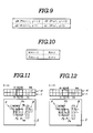
- Fig. 3 shows the relationship between the 4-bit pixel data transferred to the decision circuit 20 from the memory 18 and the 4-bit output data produced from the decision circuit 20.
- the decision circuit 20 produces 4-bit output data which are the same as the transferred 4-bit pixel data when the transferred 4-bit pixel data form a 4-connectedness pixel data matrix such as pixel data No. 3, No. 5, No. 7, No. 10, No. 11. No. 12, No. 13 or No. 14. Otherwise, the decision circuit 20 outputs 4-bit data "0000".
- Fig. 4 shows the relationship between the 4-bit pixel data transferred to the decision circuit 20 from the memory 18 and the 4-bit output data produced from the decision circuit 20.
- the decision circuit 20 produces 4-bit output data which are the same as the transferred 4-bit pixel data when the transferred 4-bit pixel data form an 8-connectedness pixel data matrix such as pixel data No. 3, No. 5, No. 6, No. 9, No. 10, No. 11, No. 12, No. 13 or No. 14. Otherwise, the decision circuit 20 outputs 4-bit data "0000".
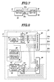
- the image contour detecting apparatus includes a contour detecting section generally designated by the numeral 30.
- the contour detecting section 30 has an input connected through the data line 12 to the scanner 10 (Fig. 1).
- the contour detecting section 30 includes a pixel data forming circuit for forming a pixel data matrix from pixel data fed thereto from the scanner.
- the contour detecting section 30 also includes a flag data matrix forming circuit which forms a flag data matrix indicating the course of the contour following process.
- the contour detecting section 30 produces command data from a relationship programmed thereinto. The relationship defines the command data as a function of pixel data matrix and flag data matrix.
- the command data are transferred to a contour analyzing section 50 which thereby provides one or more sequences of the contour forming pixels for forming the image contour.
- the contour detecting section 30 includes a pixel data memory 32 having four 1-bit memory sections.
- the pixel data memory 32 may be taken in the form of a shift register matrix consisting of a first bank including front and rear shift registers connected in series with each other and a second bank including front and rear shift registers connected in series with each other.
- the first bank front shift register has an input connected to the data line 12 and the first bank rear shift register has an output connected to a line memory 34.
- the line memory 34 has memory sections for storing pixel data regarding successive pixels in number equal to the number of pixels located on a scan line.
- the second bank front shift register has an input connected to the line memory 34.
- the symbol o indicates a requirement of producing command data through the data line 30b, causing the contour analyzing section 50 to perform a process to connect the contour forming pixels.
- the empty space indicates a requirement of producing a command signal through the signal line 30a, causing the contour analyzing section 50 to perform no process.
- the symbole ⁇ indicates the same command as indicated by the empty space. In this case, however, the command generator circuit 48 may produce command data through the data line 30b to cause the contour analyzing circuit 50 to perform a process necessary for connecting the contour forming pixels and a process necessary for run length coding.
Landscapes
- Engineering & Computer Science (AREA)
- Physics & Mathematics (AREA)
- General Physics & Mathematics (AREA)
- Theoretical Computer Science (AREA)
- Computer Vision & Pattern Recognition (AREA)
- Multimedia (AREA)
- Image Analysis (AREA)
- Image Processing (AREA)
Applications Claiming Priority (4)
| Application Number | Priority Date | Filing Date | Title |
|---|---|---|---|
| JP60744/87 | 1987-03-16 | ||
| JP62060744A JPH083849B2 (ja) | 1987-03-16 | 1987-03-16 | 輪郭画素抽出装置 |
| JP62161945A JPS647176A (en) | 1987-06-29 | 1987-06-29 | Outline detection device |
| JP161945/87 | 1987-06-29 |
Publications (3)
| Publication Number | Publication Date |
|---|---|
| EP0282972A2 true EP0282972A2 (fr) | 1988-09-21 |
| EP0282972A3 EP0282972A3 (en) | 1990-12-12 |
| EP0282972B1 EP0282972B1 (fr) | 1995-12-27 |
Family
ID=26401800
Family Applications (1)
| Application Number | Title | Priority Date | Filing Date |
|---|---|---|---|
| EP88104101A Expired - Lifetime EP0282972B1 (fr) | 1987-03-16 | 1988-03-15 | Appareil de détection de contour d'image |
Country Status (4)
| Country | Link |
|---|---|
| US (1) | US4817173A (fr) |
| EP (1) | EP0282972B1 (fr) |
| KR (1) | KR0125276B1 (fr) |
| DE (1) | DE3854822T2 (fr) |
Cited By (3)
| Publication number | Priority date | Publication date | Assignee | Title |
|---|---|---|---|---|
| US7884161B2 (en) | 2006-03-13 | 2011-02-08 | Lg Chem, Ltd. | Method for preparation of 1-alkene-acrylate based copolymer |
| RU2450355C1 (ru) * | 2011-02-22 | 2012-05-10 | Государственное образовательное учреждение высшего профессионального образования "Алтайский государственный технический университет им. И.И. Ползунова" (АлтГТУ) | Способ замыкания контуров объектов на матрице полутонового растрового изображения |
| RU2491753C1 (ru) * | 2010-12-10 | 2013-08-27 | Кэнон Кабусики Кайся | Устройство обработки изображения и способ обработки изображения |
Families Citing this family (5)
| Publication number | Priority date | Publication date | Assignee | Title |
|---|---|---|---|---|
| US5561534A (en) * | 1991-07-12 | 1996-10-01 | Canon Kabushiki Kaisha | Image processing method and apparatus |
| KR100209419B1 (ko) * | 1996-07-09 | 1999-07-15 | 전주범 | 영상신호로 표현된 객체의 윤곽선 부호화 방법 |
| KR100457064B1 (ko) * | 1997-11-13 | 2005-05-27 | 주식회사 대우일렉트로닉스 | 윤곽선정보검출방법 |
| US8994747B2 (en) * | 2007-11-09 | 2015-03-31 | Imacor Inc. | Superimposed display of image contours |
| JP2011216080A (ja) * | 2010-03-18 | 2011-10-27 | Canon Inc | 画像処理装置、画像処理方法、および記憶媒体 |
Family Cites Families (4)
| Publication number | Priority date | Publication date | Assignee | Title |
|---|---|---|---|---|
| FR2507419B1 (fr) * | 1981-06-09 | 1985-10-04 | Centre Nat Rech Scient | Procede et dispositif d'extraction de contours d'objets au moyen d'une camera video |
| JPS5851388A (ja) * | 1981-09-22 | 1983-03-26 | Ricoh Co Ltd | 方向コ−ド割付け方法 |
| GB8311813D0 (en) * | 1983-04-29 | 1983-06-02 | West G A W | Coding and storing raster scan images |
| JPS6140684A (ja) * | 1984-07-31 | 1986-02-26 | Omron Tateisi Electronics Co | 輪郭追跡装置 |
-
1988
- 1988-03-15 EP EP88104101A patent/EP0282972B1/fr not_active Expired - Lifetime
- 1988-03-15 US US07/168,372 patent/US4817173A/en not_active Expired - Fee Related
- 1988-03-15 DE DE3854822T patent/DE3854822T2/de not_active Expired - Fee Related
- 1988-03-16 KR KR1019880002757A patent/KR0125276B1/ko not_active Expired - Fee Related
Cited By (3)
| Publication number | Priority date | Publication date | Assignee | Title |
|---|---|---|---|---|
| US7884161B2 (en) | 2006-03-13 | 2011-02-08 | Lg Chem, Ltd. | Method for preparation of 1-alkene-acrylate based copolymer |
| RU2491753C1 (ru) * | 2010-12-10 | 2013-08-27 | Кэнон Кабусики Кайся | Устройство обработки изображения и способ обработки изображения |
| RU2450355C1 (ru) * | 2011-02-22 | 2012-05-10 | Государственное образовательное учреждение высшего профессионального образования "Алтайский государственный технический университет им. И.И. Ползунова" (АлтГТУ) | Способ замыкания контуров объектов на матрице полутонового растрового изображения |
Also Published As
| Publication number | Publication date |
|---|---|
| DE3854822D1 (de) | 1996-02-08 |
| EP0282972B1 (fr) | 1995-12-27 |
| US4817173A (en) | 1989-03-28 |
| EP0282972A3 (en) | 1990-12-12 |
| KR880011690A (ko) | 1988-10-29 |
| KR0125276B1 (ko) | 1997-12-15 |
| DE3854822T2 (de) | 1996-05-23 |
Similar Documents
| Publication | Publication Date | Title |
|---|---|---|
| US5757382A (en) | Apparatus for tracing contours of segmented regions | |
| US4246578A (en) | Pattern generation display system | |
| EP0115584B1 (fr) | Appareil pour la production d'images et procédé pour traiter des signaux à utiliser par un tel appareil représentants des images | |
| US4648119A (en) | Method and apparatus for forming 3×3 pixel arrays and for performing programmable pattern contingent modifications of those arrays | |
| EP0558049B1 (fr) | Méthode et appareil pour l'extraction de contours dans une image | |
| GB2174278A (en) | Area-fill graphic image processing system | |
| US5142355A (en) | Edit control system for use in an image processing apparatus | |
| EP0805587A2 (fr) | Obtention de demi-teintes sans joint en parallèle par un processus d'entourage | |
| EP0177704B1 (fr) | Dispositif de lissage pour l'affiche d'image | |
| US4817173A (en) | Image contour detecting apparatus | |
| EP0642256A2 (fr) | Système de détection de région entourée en marqueur en passage unique et procédé pour un photocopieur | |
| EP0459350A2 (fr) | Procédé et appareil pour la génération de données d'images représentant des images intégrées | |
| JP3749282B2 (ja) | 画像処理装置 | |
| US4887302A (en) | Labelling circuit for image processor | |
| EP0146229B1 (fr) | Dispositif pour agrandir des éléments d'image illuminés dans un dispositif d'affichage à T.R.C. | |
| EP0477904B1 (fr) | Méthode et appareil pour la génération d'images réduites | |
| EP0614154A2 (fr) | Procédé et appareil pour la correction d'images multi-tons | |
| US5640607A (en) | Method for sending bit mapped image by appending special code to text string and transmitting the text string separately from compressed residual image | |
| EP0091124B1 (fr) | Circuit générateur de signaux vidéo | |
| EP0284326B1 (fr) | Générateur de signaux d'affichage de configurations et appareil d'affichage utilisant ces signaux | |
| EP0648041A1 (fr) | Procédé et appareil pour modifier la base de séparation d'une figure | |
| US5606656A (en) | Image data processing unit for forming a plurality of identical images in a single output image area | |
| EP0477956B1 (fr) | Procédé et dispositif de traitement d'images pour des contours polygonaux | |
| EP0134248B1 (fr) | Dispositif d'affichage | |
| US5553204A (en) | Image output apparatus for gradation image data |
Legal Events
| Date | Code | Title | Description |
|---|---|---|---|
| PUAI | Public reference made under article 153(3) epc to a published international application that has entered the european phase |
Free format text: ORIGINAL CODE: 0009012 |
|
| AK | Designated contracting states |
Kind code of ref document: A2 Designated state(s): DE FR GB |
|
| PUAL | Search report despatched |
Free format text: ORIGINAL CODE: 0009013 |
|
| AK | Designated contracting states |
Kind code of ref document: A3 Designated state(s): DE FR GB |
|
| 17P | Request for examination filed |
Effective date: 19901228 |
|
| 17Q | First examination report despatched |
Effective date: 19921020 |
|
| GRAA | (expected) grant |
Free format text: ORIGINAL CODE: 0009210 |
|
| AK | Designated contracting states |
Kind code of ref document: B1 Designated state(s): DE FR GB |
|
| REF | Corresponds to: |
Ref document number: 3854822 Country of ref document: DE Date of ref document: 19960208 |
|
| PGFP | Annual fee paid to national office [announced via postgrant information from national office to epo] |
Ref country code: GB Payment date: 19960226 Year of fee payment: 9 |
|
| PGFP | Annual fee paid to national office [announced via postgrant information from national office to epo] |
Ref country code: FR Payment date: 19960318 Year of fee payment: 9 |
|
| ET | Fr: translation filed | ||
| PGFP | Annual fee paid to national office [announced via postgrant information from national office to epo] |
Ref country code: DE Payment date: 19960426 Year of fee payment: 9 |
|
| PLBE | No opposition filed within time limit |
Free format text: ORIGINAL CODE: 0009261 |
|
| STAA | Information on the status of an ep patent application or granted ep patent |
Free format text: STATUS: NO OPPOSITION FILED WITHIN TIME LIMIT |
|
| 26N | No opposition filed | ||
| PG25 | Lapsed in a contracting state [announced via postgrant information from national office to epo] |
Ref country code: GB Effective date: 19970315 |
|
| GBPC | Gb: european patent ceased through non-payment of renewal fee |
Effective date: 19970315 |
|
| PG25 | Lapsed in a contracting state [announced via postgrant information from national office to epo] |
Ref country code: FR Free format text: LAPSE BECAUSE OF NON-PAYMENT OF DUE FEES Effective date: 19971128 |
|
| PG25 | Lapsed in a contracting state [announced via postgrant information from national office to epo] |
Ref country code: DE Effective date: 19971202 |
|
| REG | Reference to a national code |
Ref country code: FR Ref legal event code: ST |