EP0283623A2 - Supraleitender Josephson-Übergang - Google Patents
Supraleitender Josephson-Übergang Download PDFInfo
- Publication number
- EP0283623A2 EP0283623A2 EP87310250A EP87310250A EP0283623A2 EP 0283623 A2 EP0283623 A2 EP 0283623A2 EP 87310250 A EP87310250 A EP 87310250A EP 87310250 A EP87310250 A EP 87310250A EP 0283623 A2 EP0283623 A2 EP 0283623A2
- Authority
- EP
- European Patent Office
- Prior art keywords
- layer
- atomic
- nbn
- mgo
- pseudo
- Prior art date
- Legal status (The legal status is an assumption and is not a legal conclusion. Google has not performed a legal analysis and makes no representation as to the accuracy of the status listed.)
- Granted
Links
Images
Classifications
-
- H—ELECTRICITY
- H10—SEMICONDUCTOR DEVICES; ELECTRIC SOLID-STATE DEVICES NOT OTHERWISE PROVIDED FOR
- H10N—ELECTRIC SOLID-STATE DEVICES NOT OTHERWISE PROVIDED FOR
- H10N60/00—Superconducting devices
- H10N60/10—Junction-based devices
- H10N60/12—Josephson-effect devices
-
- H—ELECTRICITY
- H10—SEMICONDUCTOR DEVICES; ELECTRIC SOLID-STATE DEVICES NOT OTHERWISE PROVIDED FOR
- H10N—ELECTRIC SOLID-STATE DEVICES NOT OTHERWISE PROVIDED FOR
- H10N60/00—Superconducting devices
- H10N60/01—Manufacture or treatment
- H10N60/0912—Manufacture or treatment of Josephson-effect devices
Definitions
- This invention relates to superconducting Josephson junctions.
- the state of the art design for a Josephson tunnel junction for superconducting electronics is a trilayer, on a substrate, formed of a layer of superconducting niobium nitride (NbN), an insulating layer of magnesium oxide (MgO), and a second layer of niobium nitride on top. While this structure is operable, it is not optimal because the lattice spacing of magnesium oxide does not match the lattice spacing of niobium nitride, although they do have the same structure and crystal orientation.
- Niobium nitride has a B1 (sodium chloride) structure with a lattice constant, (a0) of 4.38 angstroms; magnesium oxide and calcium oxide have the same B1 structure, but magnesium oxide has a lattice constant of 4.21 angstroms. Because of this mismatch, the initial layer of the top niobium nitride will be partly disordered, the superconducting energy gap reduced, and the operating temperature of the junction reduced.
- the present invention resides in a superconducting Josephson junction comprising (A) a layer of NbN on a substrate; (B) a solid solution of an epitaxial layer of a pseudo-binary compound on said layer of NbN, said solid solution lying between 3 atomic % MgO and 97 atomic % CaO, and 97 atomic % MgO and 3 atomic % CaO; and (C) an epitaxial layer of NbN on said layer of pseudo-binary compound.
- the invention also includes a method of making a superconducting Josephson junction characterized by (A) depositing a layer of NbN onto a suitable substrate; (B) depositing an epitaxial layer of a pseudo-binary compound onto said layer of NbN, where said compound comprises from 3 atomic % MgO and 97 atomic % CaO, to 97 atomic % MgO and 3 atomic % CaO; and (C) depositing an epitaxial layer of NbN onto said layer of said compound.
- a superconducting Josephson junction can be formed from a pseudo-binary solid solution of magnesium and calcium oxides sandwiched between two niobium nitride layers.
- Calcium oxide has the same B1 structure as MgO but a lattice constant of 4.84 angstroms.
- the Josephson junctions of this invention have a more uniform oxide layer than do the Josephson junctions formed with MgO. (Theoretical and experimental background for such a claim is found in J. W. Mathews et al., "Effect of Coherency Strain and Misfit Dislocations on the Mode of Growth of Thin Films," Thin Solid Films 26 pp. 129-134 (1975).)
- the superior oxide layer of this invention results in a better quality niobium nitride top layer on the oxide layer.
- the oxide layer of this invention has the same lattice spacing as the niobium nitride layer, we are able to obtain a very good quality niobium nitride top layer. As a result, the superconducting transition temperature of the niobium nitride layer is higher.
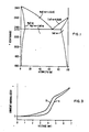
- the equilibrium phase diagram shown in Figure 1 was taken from an article by R. C. Doman et al. in the Journal of the American Ceramics Society , July, 1983, titled "Phase Equilibria in the System CaO-MgO," which is herein incorporated by reference.
- the ordinate gives the temperature in degrees centigrade and the abscissa gives the atomic percent of calcium oxide in the MgO-CaO system.
- the phase diagram shows that below a temperature of 2370°C, separate solid solutions (SS) of magnesium oxide and calcium oxide form, and that below 1600°C no mixed solid solutions of magnesium oxide and calcium oxide exist where the amount of calcium oxide is greater than 2% or less than 98%.
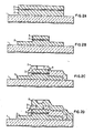
- a substrate 1 has deposited thereon a base electrode 2 of niobium nitride, a barrier layer 3 of the pseudo-binary compound, and a counterelectrode 4 also of niobium nitride.
- a base electrode 2 of niobium nitride In Figure 2B portions of the counterelectrode barrier layer and base electrode have been etched away.
- a contact layer 6, also of niobium nitride has been deposited.
- any substrate material that can provide mechanical support for the junction and that helps to promote growth of niobium nitride can be used in this invention.
- the preferred materials are sapphire ( ⁇ -Al2O3) or magnesium oxide (MgO) as these materials closely match the lattice spacing of niobium nitride.
- the substrate may be of any size and thickness but is typically about 6 millimeters square to about 2 inches diameter and about 20 mils thick.
- the substrate may have any orientation, but we have found that the (100) orientation of a magnesium oxide substrate produces smooth single-crystal layers. Also, we have found that the (111) niobium nitride single-crystal films grown on a sapphire substrate had the best junction properties.
- the (111) niobium nitride orientation can be obtained if the sapphire orientation is (11 2 0) or (0001). Sapphire is preferred to magnesium oxide as a substrate because it is more available and easier to use.
- the first step is to deposit a layer of niobium nitride on the substrate.
- This can be accomplished, for example, by chemical vapor deposition or sputtering, processes that are well known in the art.
- chemical vapor deposition a niobium-containing gas is passed over a hot surface causing a reaction to occur that forms niobium nitride, which deposits upon the substrate.
- Either radio frequency (RF) sputtering or direct current (DC) sputtering can also be used, but reactive DC sputtering is preferred as it produces a higher superconducting transition temperature.
- Reactive DC sputtering is performed by sputtering niobium in a gas containing nitrogen and argon (and no oxygen), where the niobium reacts with the nitrogen to form niobium nitride at the substrate.
- a gas containing nitrogen and argon (and no oxygen) where the niobium reacts with the nitrogen to form niobium nitride at the substrate.
- the conditions for depositing a single crystal niobium nitride superconductor by DC magnetron sputtering are reported in the literature. See, for example, V. L. Noskov et al., Soviet Physics Crystallography, 25(4), 504 (1980).
- the niobium nitride layers may be either polycrystalline or single crystal, but single crystal layers are preferred as they are easier to test.
- the niobium nitride layer may be from 400 angstroms to 5000 angstroms thick, and is preferably from 1500 to 2500 angstroms thick. If the niobium nitride layer is too thick, it becomes difficult to cover the steps that are formed when the layers are etched; and if the niobium nitride layer is too thin, the speed of the circuit decreases. The thickness of the layer is determined by the deposition time.
- a layer of the pseudo-binary compound is deposited upon the layer of niobium nitride; the pseudo-binary compound grows on the layer of niobium nitride by single crystal epitaxy and has the same structure as the layer of niobium nitride.
- the composition of the pseudo-binary compound can vary from 3 atomic percent MgO and 97 atomic percent CaO to 97 atomic percent MgO and 3 atomic percent CaO.
- a preferred range is from 22 to 35 atomic percent CaO (and the remainder, MgO) because we have determined by calculation that the optimal composition is 0.73 atomic percent MgO-0.27 atomic percent CaO, and this range gives a lattice spacing mismatch of 1% or less.
- the layer of pseudo-binary compound can be deposited, for example, by RF sputtering or by evaporation. Evaporation is accomplished by heating an appropriate mixture of MgO-CaO above the melting point of MgO (2800°C). It should be noted that the composition of the layer of pseudo-binary compound may not be exactly the same as the composition of the material which was used to form the layer due to differences in vapor pressure between the magnesium oxide and calcium oxide as they are being evaporated.
- the composition of the starting material can be adjusted to obtain the desired composition of the deposited layer.
- the thickness of the insulating layer of pseudo-binary compound is preferably about 5 to about 25 angstroms as thinner layers may result in superconducting shorts, and thicker layers have greater resistance which reduces the circuit speed.
- the second niobium nitride layer is deposited upon the layer of pseudo-binary compound.
- the deposition process and parameters for that layer can be the same as for the first layer of niobium nitride.
- various processes can be used, as is well known in the art, to form circuit patterns and attach connections. These processes include etching, the application of photoresists, the development of photoresist to form circuit patterns, and the deposition of contact layers.
- the Josephson junctions of this invention in addition to being used in superconducting computers, can also be used in other types of apparatus such as radar signal processing apparatus.
- a polished single-crystal sapphire plate 1/4 inch by 1/4 inch by 20 mils thick having a (11 2 0) orientation was placed in a DC magnetron and was heated to 700°C.
- niobium nitride was sputtered onto the substrate a rate of 40 angstroms per minute.
- the resulting film was about 1,000 angstroms thick and had a (111) crystal orientation.
- a barrier layer was deposited on the niobium nitride layer from a mixture of 73 mole percent magnesium oxide -- 27 mole percent calcium oxide using RF magnetron sputtering in pure argon at 7 mtorr. The deposition rate was 6 angstroms a minute and the barrier film was about 20 angstroms thick.
- the temperature of the coated substrate was cooled to 150°C and the counter electrode was deposited in the same manner as the base electrode at the same deposition rate.
- the counter electrode was about 500 angstroms thick and had a (111) crystal orientation.
- a photoresist was spun onto a substrate and was exposed and developed to define a junction area. The exposed area was etched using reactive ion etching down to the base electrode as shown in Figure 2B. A second layer of photoresist was applied, leaving an opening for contact to the top electrode. This photoresist was left in place as an insulator as shown in Figure 2C. Finally, a contact layer of niobium nitride was applied as shown in Figure 2D in the same manner as the other layers of niobium nitride.
- the completed Josephson junction was tested in a magnetically shielded dewar filled with liquid helium at 4.2°K by passing a slowly increasing current through it while measuring the voltage. When the voltage had increased to about 7 millivolts, the experiment was terminated.
- Figure 3 is a graph of current versus voltage which gives the results of this experiment.
- the graph proves that conduction through the Josephson junction was by tunnelling rather than by metal conduction.
- the graph also shows that the slope of Curve A, the mixed oxide, was highest at a voltage of 4.8 millivolts (the gap voltage). This compares very favorably with the gap voltage of a typical Josephson junction using a magnesium oxide barrier layer, Curve B, which has a gap voltage of 4.5 millivolts.
- the significantly higher gap voltage indicates that the Josephson junction of this invention will be able to operate at a higher superconducting transition temperature since the gap voltage is directly proportional to the transition temperature: where V g equals the gap voltage, k B equals Boltzmann's constant and, and T c is the superconducting transition temperature.
Landscapes
- Engineering & Computer Science (AREA)
- Manufacturing & Machinery (AREA)
- Superconductor Devices And Manufacturing Methods Thereof (AREA)
Applications Claiming Priority (2)
| Application Number | Priority Date | Filing Date | Title |
|---|---|---|---|
| US30003 | 1981-12-11 | ||
| US07/030,003 US4768069A (en) | 1987-03-23 | 1987-03-23 | Superconducting Josephson junctions |
Publications (3)
| Publication Number | Publication Date |
|---|---|
| EP0283623A2 true EP0283623A2 (de) | 1988-09-28 |
| EP0283623A3 EP0283623A3 (en) | 1989-03-22 |
| EP0283623B1 EP0283623B1 (de) | 1992-12-30 |
Family
ID=21852020
Family Applications (1)
| Application Number | Title | Priority Date | Filing Date |
|---|---|---|---|
| EP87310250A Expired EP0283623B1 (de) | 1987-03-23 | 1987-11-19 | Supraleitender Josephson-Übergang |
Country Status (6)
| Country | Link |
|---|---|
| US (1) | US4768069A (de) |
| EP (1) | EP0283623B1 (de) |
| JP (1) | JP2623100B2 (de) |
| DE (1) | DE3783359T2 (de) |
| ES (1) | ES2043670T3 (de) |
| IL (1) | IL85491A (de) |
Cited By (1)
| Publication number | Priority date | Publication date | Assignee | Title |
|---|---|---|---|---|
| GB2217943B (en) * | 1988-04-22 | 1992-12-23 | Nat Res Dev | Epitaxial deposition. |
Families Citing this family (13)
| Publication number | Priority date | Publication date | Assignee | Title |
|---|---|---|---|---|
| US5362709A (en) * | 1988-09-22 | 1994-11-08 | Semiconductor Energy Laboratory, Co., Ltd. | Superconducting device |
| JPH02177381A (ja) * | 1988-09-22 | 1990-07-10 | Semiconductor Energy Lab Co Ltd | 超伝導体のトンネル接合素子 |
| JP2508259B2 (ja) * | 1989-04-13 | 1996-06-19 | 日本電気株式会社 | 超伝導三端子素子およびその製造方法 |
| US5100694A (en) * | 1989-08-01 | 1992-03-31 | The United States Of America As Represented By The Administrator National Aeronautics And Space Administration | Method for producing edge geometry superconducting tunnel junctions utilizing an NbN/MgO/NbN thin film structure |
| US5099294A (en) * | 1989-08-01 | 1992-03-24 | The United States Of America As Represented By The Administrator Of The National Aeronautics And Space Administration | Edge geometry superconducting tunnel junctions utilizing an NbN/MgO/NbN thin film structure |
| JPH03259576A (ja) * | 1990-03-09 | 1991-11-19 | Sumitomo Electric Ind Ltd | ジョセフソン接合 |
| US6784139B1 (en) * | 2000-07-10 | 2004-08-31 | Applied Thin Films, Inc. | Conductive and robust nitride buffer layers on biaxially textured substrates |
| US7060508B2 (en) * | 2003-02-12 | 2006-06-13 | Northrop Grumman Corporation | Self-aligned junction passivation for superconductor integrated circuit |
| US7615385B2 (en) | 2006-09-20 | 2009-11-10 | Hypres, Inc | Double-masking technique for increasing fabrication yield in superconducting electronics |
| US9929334B2 (en) * | 2015-01-15 | 2018-03-27 | International Business Machines Corporation | Josephson junction with spacer |
| CN105449094B (zh) * | 2015-12-29 | 2019-04-05 | 中国科学院上海微系统与信息技术研究所 | 氮化铌薄膜的制备方法、squid器件及其制备方法 |
| US12161052B2 (en) | 2018-03-06 | 2024-12-03 | Cornell University | Expitaxial semiconductor/superconductor heterostructures |
| US11563162B2 (en) * | 2020-01-09 | 2023-01-24 | International Business Machines Corporation | Epitaxial Josephson junction transmon device |
Family Cites Families (8)
| Publication number | Priority date | Publication date | Assignee | Title |
|---|---|---|---|---|
| FR2071706A5 (de) * | 1969-11-12 | 1971-09-17 | Ibm | |
| US3999203A (en) * | 1974-03-29 | 1976-12-21 | International Business Machines Corporation | Josephson junction device having intermetallic in electrodes |
| US4242419A (en) * | 1977-12-29 | 1980-12-30 | Bell Telephone Laboratories, Incorporated | Epitaxial growth of superconductors such as Nb3 Ge superconductors |
| US4316785A (en) * | 1979-11-05 | 1982-02-23 | Nippon Telegraph & Telephone Public Corporation | Oxide superconductor Josephson junction and fabrication method therefor |
| DE3161996D1 (en) * | 1980-02-20 | 1984-03-01 | Fujitsu Ltd | Superconductive logic device incorporating a josephson junction |
| JPS5734073A (en) * | 1980-07-31 | 1982-02-24 | Harima Refractories Co Ltd | Magnesia-carbon refractories |
| US4432134A (en) * | 1982-05-10 | 1984-02-21 | Rockwell International Corporation | Process for in-situ formation of niobium-insulator-niobium Josephson tunnel junction devices |
| US4499119A (en) * | 1983-07-06 | 1985-02-12 | Sperry Corporation | Method of manufacturing super-conductive tunnel junction devices with precise junction area control |
-
1987
- 1987-03-23 US US07/030,003 patent/US4768069A/en not_active Expired - Lifetime
- 1987-11-19 DE DE8787310250T patent/DE3783359T2/de not_active Expired - Lifetime
- 1987-11-19 ES ES87310250T patent/ES2043670T3/es not_active Expired - Lifetime
- 1987-11-19 EP EP87310250A patent/EP0283623B1/de not_active Expired
- 1987-11-24 JP JP62297300A patent/JP2623100B2/ja not_active Expired - Fee Related
-
1988
- 1988-02-22 IL IL85491A patent/IL85491A/xx not_active IP Right Cessation
Non-Patent Citations (2)
| Title |
|---|
| APPLIED PHYSICS LETTERS, vol. 46, no. 11, 1st June 1985, pages 1098-1099, American Institute of Physics, New York, US; A. SHOJI et al.: "Niobium nitride Josephson tunnel junctions with magnesium oxide barriers" * |
| IEEE TRANSACTIONS ON MAGNETICS, vol. MAG-23, no. 2, March 1987, pages 1464-1471, IEEE, New York, US; A. SHOJI et al.: "Temperature-dependent properties of niobium nitride Josephson tunnel junctions" * |
Cited By (1)
| Publication number | Priority date | Publication date | Assignee | Title |
|---|---|---|---|---|
| GB2217943B (en) * | 1988-04-22 | 1992-12-23 | Nat Res Dev | Epitaxial deposition. |
Also Published As
| Publication number | Publication date |
|---|---|
| EP0283623A3 (en) | 1989-03-22 |
| ES2043670T3 (es) | 1994-01-01 |
| EP0283623B1 (de) | 1992-12-30 |
| JPS6439085A (en) | 1989-02-09 |
| DE3783359D1 (de) | 1993-02-11 |
| IL85491A (en) | 1991-06-10 |
| JP2623100B2 (ja) | 1997-06-25 |
| DE3783359T2 (de) | 1993-04-15 |
| US4768069A (en) | 1988-08-30 |
| IL85491A0 (en) | 1988-07-31 |
Similar Documents
| Publication | Publication Date | Title |
|---|---|---|
| Scheel et al. | Problems in epitaxial growth of high-Tc superconductors | |
| JP3275836B2 (ja) | 超電導デバイス | |
| EP0283623B1 (de) | Supraleitender Josephson-Übergang | |
| EP0382609B1 (de) | Verfahren zur Herstellung von Josephson-Übergängen | |
| US4874741A (en) | Non-enhanced laser evaporation of oxide superconductors | |
| JPH01161881A (ja) | ジョセフソン素子およびその製造方法 | |
| US5982034A (en) | Conductive oxide films | |
| AU655656B2 (en) | Process for making superconducting Tl-Pb-Sr-Ca-Cu oxide films and devices | |
| JPH04300292A (ja) | 複合酸化物超電導薄膜の成膜方法 | |
| Geerk et al. | HTSC thin film growth by inverted cylindrical magnetron sputtering | |
| US5364836A (en) | Article comprising a superconductor/insulator layer structure, and method of making the article | |
| Kimura et al. | Bi-Sr-Ca-Cu-O film on sapphire grown by plasma-enhanced halide CVD | |
| US5252390A (en) | Laminated film | |
| JPS63225599A (ja) | 酸化物超伝導薄膜の作製方法 | |
| JP2907831B2 (ja) | ジョセフソン素子 | |
| JPH0278282A (ja) | ジヨセフソン素子 | |
| JP2852753B2 (ja) | 酸化物超伝導素子および酸化物超伝導体薄膜の製造方法 | |
| JP3379533B2 (ja) | 超電導デバイスの製造方法 | |
| JPH02107597A (ja) | 酸化物超伝導体を基板に付着させる方法 | |
| Chen et al. | Solid phase epitaxy of Bi2Sr2CaCu2O x superconducting thin films | |
| JP2844206B2 (ja) | 酸化物超伝導素子および酸化物超伝導体薄膜の製造方法 | |
| JP2844207B2 (ja) | 酸化物超伝導素子および酸化物超伝導体薄膜の製造方法 | |
| Fröhlich et al. | MOCVD of YBa2Cu3O7− x thin films using a Ba fluorocarbon-based precursor | |
| JP2757257B2 (ja) | 酸化物超伝導薄膜の形成方法 | |
| JP3068917B2 (ja) | 超電導デバイス |
Legal Events
| Date | Code | Title | Description |
|---|---|---|---|
| PUAI | Public reference made under article 153(3) epc to a published international application that has entered the european phase |
Free format text: ORIGINAL CODE: 0009012 |
|
| AK | Designated contracting states |
Kind code of ref document: A2 Designated state(s): DE ES FR GB IT |
|
| PUAL | Search report despatched |
Free format text: ORIGINAL CODE: 0009013 |
|
| AK | Designated contracting states |
Kind code of ref document: A3 Designated state(s): DE ES FR GB IT |
|
| 17P | Request for examination filed |
Effective date: 19890919 |
|
| 17Q | First examination report despatched |
Effective date: 19911204 |
|
| GRAA | (expected) grant |
Free format text: ORIGINAL CODE: 0009210 |
|
| AK | Designated contracting states |
Kind code of ref document: B1 Designated state(s): DE ES FR GB IT |
|
| ET | Fr: translation filed | ||
| REF | Corresponds to: |
Ref document number: 3783359 Country of ref document: DE Date of ref document: 19930211 |
|
| ITF | It: translation for a ep patent filed | ||
| PLBE | No opposition filed within time limit |
Free format text: ORIGINAL CODE: 0009261 |
|
| STAA | Information on the status of an ep patent application or granted ep patent |
Free format text: STATUS: NO OPPOSITION FILED WITHIN TIME LIMIT |
|
| 26N | No opposition filed | ||
| REG | Reference to a national code |
Ref country code: ES Ref legal event code: FG2A Ref document number: 2043670 Country of ref document: ES Kind code of ref document: T3 |
|
| REG | Reference to a national code |
Ref country code: GB Ref legal event code: IF02 |
|
| PGFP | Annual fee paid to national office [announced via postgrant information from national office to epo] |
Ref country code: FR Payment date: 20061117 Year of fee payment: 20 |
|
| PGFP | Annual fee paid to national office [announced via postgrant information from national office to epo] |
Ref country code: GB Payment date: 20061122 Year of fee payment: 20 |
|
| PGFP | Annual fee paid to national office [announced via postgrant information from national office to epo] |
Ref country code: ES Payment date: 20061124 Year of fee payment: 20 |
|
| PGFP | Annual fee paid to national office [announced via postgrant information from national office to epo] |
Ref country code: IT Payment date: 20061130 Year of fee payment: 20 |
|
| PGFP | Annual fee paid to national office [announced via postgrant information from national office to epo] |
Ref country code: DE Payment date: 20070102 Year of fee payment: 20 |
|
| REG | Reference to a national code |
Ref country code: GB Ref legal event code: PE20 |
|
| REG | Reference to a national code |
Ref country code: ES Ref legal event code: FD2A Effective date: 20071120 |
|
| PG25 | Lapsed in a contracting state [announced via postgrant information from national office to epo] |
Ref country code: GB Free format text: LAPSE BECAUSE OF EXPIRATION OF PROTECTION Effective date: 20071118 Ref country code: ES Free format text: LAPSE BECAUSE OF EXPIRATION OF PROTECTION Effective date: 20071120 |