EP0284060B1 - Dispositif pour sélectionner la condition de test d'une microplaquette - Google Patents
Dispositif pour sélectionner la condition de test d'une microplaquette Download PDFInfo
- Publication number
- EP0284060B1 EP0284060B1 EP88104730A EP88104730A EP0284060B1 EP 0284060 B1 EP0284060 B1 EP 0284060B1 EP 88104730 A EP88104730 A EP 88104730A EP 88104730 A EP88104730 A EP 88104730A EP 0284060 B1 EP0284060 B1 EP 0284060B1
- Authority
- EP
- European Patent Office
- Prior art keywords
- signals
- selector
- signal
- decoder
- signal bus
- Prior art date
- Legal status (The legal status is an assumption and is not a legal conclusion. Google has not performed a legal analysis and makes no representation as to the accuracy of the status listed.)
- Expired - Lifetime
Links
Images






Classifications
-
- G—PHYSICS
- G06—COMPUTING OR CALCULATING; COUNTING
- G06F—ELECTRIC DIGITAL DATA PROCESSING
- G06F13/00—Interconnection of, or transfer of information or other signals between, memories, input/output devices or central processing units
-
- G—PHYSICS
- G06—COMPUTING OR CALCULATING; COUNTING
- G06F—ELECTRIC DIGITAL DATA PROCESSING
- G06F9/00—Arrangements for program control, e.g. control units
- G06F9/06—Arrangements for program control, e.g. control units using stored programs, i.e. using an internal store of processing equipment to receive or retain programs
- G06F9/22—Microcontrol or microprogram arrangements
- G06F9/26—Address formation of the next micro-instruction ; Microprogram storage or retrieval arrangements
- G06F9/262—Arrangements for next microinstruction selection
- G06F9/264—Microinstruction selection based on results of processing
Definitions
- This invention relates to integrated circuit chip devices and more particularly to selecting signals from a plurality of sources located on an integrated circuit chip.
- next address generation or branching circuits have been implemented using combinations of matrices or multiplexer circuits.
- An example of such an arrangement is disclosed in U.S. Patent No. 3,955,180. While this approach has been useful in implementing microprogrammed processors constructed from discrete components, it can be wasteful of chip area unless the sources of the signals requiring examination are concentrated within a few areas.
- the present invention provides for the on-chip selection of signals received from a large number of sources which are distributed throughout the area of a microprocessor integrated circuit chip.
- the area of the chip is divided into a plurality of functional areas or regions.
- a decoder circuit is strategically located in at least one functional area as close as possible to the sources of signals within the area.
- a plurality of lines of an access bus are distributed throughout the chip functional areas as a function of the concentration of the source signals within each area for transmitting the source signals to a predetermined part of the chip for final selection.
- the apparatus of the invention further includes a number of pluralities of linking switches, each plurality for connecting the sources of a functional area to the access bus.
- the linking switches which are constructed from pass transistors are enabled by signals from its associated decoder circuit to apply source signals to the access bus lines.
- Each decoder circuit is connected in common to a control bus which distributes a set of control signals to all decoder circuits.
- the set of control signals corresponds to a predetermined portion of a test control field of the chip's microinstruction word.
- the control bus is positioned adjacent to the access bus.
- the access bus lines are terminated in a selector circuit.
- the selector circuit in response to signals from an associated selector decoder circuit, selects the final output signal from one of the sources specified by the test control field for use by the chip's address generation circuits in selecting the next microinstruction to be executed by the microprocessor.
- the selector decoder circuit is connected to receive other signals from the test control field in addition to signals from indicator storage circuits which define the type of operation currently being performed by the microprocessor. This is done in order to service local conditions and to resolve any testing conflicts.
- the microprocessor chip includes separate processors for executing binary, decimal and floating point operations.
- the types of operations performed by these processors are described in the related copending patent application of Thomas F. Joyce, et al. titled, "Microprocessors on a Single Semiconductor Chip".
- the decoders associated with the areas enable their respective linking switches to apply signals from the corresponding sources to different predetermined ones of the access bus lines for final selection by the selector circuit.
- the selector decoder As a function of the type of operation being performed and the states of the signals from the test control field, the selector decoder generates an output signal which conditions the selector circuit to select the bus access line which is to provide the final source signal to be examined or tested by the microprocessor next address generation circuits. Additionally, the selector circuit also includes input means for enabling the selection of signals from local sources which do not require connection to the access bus. Thus, the arrangement of the present invention also provides for the selection of signals from localized as well as remotely located sources.
- the arrangement of the present invention reduces considerably, the chip area required to carry out the selection of a source signal from the large number of sources widely distributed throughout the chip. Since each line of the access bus can be assigned a number of source signals, this provides additional flexibility. In the preferred embodiment, the number of source signals which can be connected to each line corresponds to 2 n wherein n is the number of bits of the test field decoded by the decoder circuits.
- the use of redundant decoder circuits minimizes the number of interconnections required to be made to the decoder output lines. It has been found that the use of such strategically placed decoder circuits minimizes the amount of chip area in contrast to having to distribute the output lines of a single decoder.
- the arrangement of the present invention provides for a large number of possible source signal selections corresponding to the number of bus access lines times 2 n . While not all of the possible assignments of each line may be required, the arrangement provides added flexibility in handling source signal conflicts.
- the number of lines included in the access bus corresponds to the maximum number of signals which can occur within a given microprocessor cycle of operation.
- Figure 1 is a block diagram illustrating the floor plan or layout of the chip which incorporates the teachings of the present invention.
- FIG. 1 shows in greater detail, the construction of the chip of Figure 1.
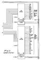
- FIG. 3 shows in greater detail, the organization of the on-chip selection apparatus of the present invention.
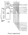
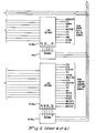
- FIGS 4a through 4d show in greater detail, different portions of the apparatus of the present invention shown in Figure 2.
- FIG. 5 shows the microinstruction word format used in conjunction with the present invention.
- FIG. 1 illustrates the functional layout of an integrated circuit microprocessor chip 10 which incorporates the principles of the present invention.
- Chip 10 includes within it a plurality of defined functional areas or sections containing the different functional elements which comprise microprocessor 10.
- the major functional areas or sections include a prefetch area 10-1, a general, CIP and SIP indicator area 10-4, a register file area 10-5, a SIP area 10-8, a CIP area 10-10, a binary ALU and shifter area 10-12 and a counter area 10-14.
- Other areas of chip 10 include the ROS control area 10-20, a major branch area 10-22, a BP port area 10-24, in addition to data selection areas 10-7 and 10-13.
- the prefetch area 10-1 includes an instruction prefetch unit for prefetching instructions from a cache or main memory.
- the SIP area 10-8 includes a scientific instruction processor (SIP) for performing scientific operations involving floating point exponent operations
- the CIP area 10-10 includes a commercial instruction processor (CIP) for performing commercial operations involving decimal operands
- the binary add and shifter area 10-12 includes a binary processing unit and shifter unit for processing binary and hexadecimal operands.
- the indicator area 10-4 includes the indicators used by the binary, CIP and SIP processors.
- the register file area 10-6 includes file addressing circuits and a plurality of register files for storing operands, exponents and work register information.
- the counter area 10-14 includes a program counter and five other counters used by the different processors.
- ROS control area 10-20 includes the various register flip-flops for storing the bits of each microinstruction word read out of a read only store (ROS) located off chip and the next address logic circuits for generating the ROS address specifying the next microinstruction word to be read out from the ROS and transferred to chip 10 for execution.
- Area 10-20 also receives signals from a pair of mode flip-flops CF6 and CF7 which store information defining the type of operation being performed by microprocessor chip 10.
- the CF6 and CF7 flip-flops are part of a CF (0-7) register which resides in indicator area 10-4.
- the CF6 and CF7 flip-flops are used by ROS control area 10-20, for purposes not related to testing, as well as by the test branch area 10-30.
- chip 10 of the preferred embodiment includes a test branch area 10-30.
- the front of this area runs vertically along functional areas 10-6 through 10-14 and has two legs which extend outward in a horizontal direction at points located near the middle and at the rear of chip 10.
- the first leg is located adjacent to functional areas 10-2 and 10-4 while the second leg is located near functional areas 10-20 and 10-22 as shown.
- the test branch area is located close to the signal sources included within the functional areas as a function of the concentration of the signals being provided by the sources.
- the rear portion of test branch area 10-30 is positioned close to ROS control area 10-20 which receives the final output signal provided by the selection circuits of the present invention included within area 10-30.
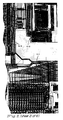
- Figure 2 shows in greater detail, the construction of certain portions of chip 10.
- the various functional areas are designated by the same reference numbers as used in Figure 1.
- the various elements included within test branch area 10-30 are also outlined in Figure 2. These elements are illustrated in schematic form in Figure 3.
- the test branch area 10-30 includes a 17 line access bus 10-300, a control bus 10-301, a back end selector circuit 10-302, a back end selector decoder circuit 10-304, a plurality of decoder circuits 10-306a through 10-306e and a plurality of linking switches 10-308a through 10-308f.
- a different one of the decoder circuits 10-306 is strategically located adjacent a different functional area as shown in Figure 3.
- the linking switches 10-308 are positioned adjacent to each decoder close to the signal sources. These switches are used to link or connect the signal sources within a functional area to access bus 10-300.
- Each of the decoder circuits 10-306a through 10-306e connect in common to control bus 10-301 at different points as shown. Signals corresponding to ROS data register bits 6-8 are applied to control bus 10-301 from the flip-flop register stages of a ROS data register which are distributed along the periphery of chip 10 as shown in Figure 1.
- the back end selector 10-302 terminates access bus 10-300 as shown and is connected to receive as inputs, the outputs of selector decoder 10-304. Additionally, the selector 10-302 has additional inputs which connect to local signal sources included within major branch area 10-22.
- the selector decoder 10-304 is connected to receive as inputs, signals corresponding to ROS data register bits 3-8 from area 10-20 and signals equivalent to those of mode control flip-flops CF6 and CF7 from indicator area 10-4.
- the arrangement of elements which comprise the on-chip selector network of the present invention simplify chip layout while at the same time are constructed so as not to affect microprocessor performance.
- the lines of the access bus 10-300 and control bus 10-301 are constructed from metal lines.
- the line connections between the linking switches 10-308 and access bus 10-300 are constructed from polysilicide material eliminating the need for an additional chip layer while still providing the required transmission speed.
- the specific series of related images which represent the three dimensional pattern or topography of semiconductor chip 10 do not form a part of the present invention but are protected as a mask work under the Semiconductor Chip Protection Act of 1984.
- Figure 4a shows a representative portion of link switches 10-308e which includes a plurality of enhancement FET devices or pass transistors 10-3082 through 10-3088.
- Each FET connects or links a different source within the prefetch unit to one of the access bus lines TBR0 through TBR16.
- more than one source i.e., FR0 through FR12
- the maximum number of sources which can connect to a single line is a function of the number of decoder outputs or 2 n where n is the number of control bus inputs.
- the control terminal of each pass transistor connects to one of the output terminals of its associated decoder (i.e., 10-306e).
- FIG. 4b illustrates a representative section of decoder 10-306.
- decoder 10-306 is constructed as a programmable logic array (PLA) using enhancement, native and depletion mode FETS.
- PLA programmable logic array
- the signals corresponding to RDR bits 6-8 are decoded to produce an output on any one of eight output lines SEL0 through SEL7.
- Figure 4c illustrates the construction of selector decoder 10-304.
- the input signals from the mode control flip-flops and RDR register stages CF6 through RDR8 are applied to a corresponding number of input buffer circuits. These circuits produce pairs of complementary outputs which are applied to the control terminals of certain enhancement mode FETS arranged in a matrix array.
- the decoder 10-304 decodes the eight input signals into 23 unique outputs for enabling selector 10-302 of Figure 4d.
- selector 10-302 includes a plurality of enhancement mode FETS, each having its control terminal connected to a different one of the outputs of selector decoder 10-304 and its drain terminal connected to either a different one of access bus lines 10-300 or one of the local sources within major branch area 10-22 as shown.
- the source terminal of each FET connects in common to the input of a buffer circuit which also connects to a voltage source VCC through a depletion FET as shown.
- the buffer circuit is connected to provide an output signal on output line TB which corresponds to the selection of a final signal source.
- the line TB connects as an input to the microprocessor's next address logic circuits.
- the numerical values included in Figures 4a through 4d represent the ratios selected for constructing the different FETS to meet the desired performance requirements of chip 10.
- circuits shown in Figures 4a through 4d can also be constructed from standard integrated circuit elements.
- the on-chip selector of the present invention is designed to select for testing, a single condition from a large number of possible conditions.
- each line of access bus 10-300 is arranged to be selected as a function of the states of mode control flip-flops CF6 and CF7 and RDR bits 3-6. The selection of these lines is accomplished as shown in the following table.
- the off-chip ROS reads out a 67-bit microinstruction word which includes a test selection field shown in Figure 5. This word is transferred to the RDR register stages within chip 10. RDR bits 6-8 are applied to the lines of control bus 10-301.
- each of the decoders 10-306a through 10-306e is identically enabled to force the same one of its output terminals to a binary ONE state.
- This in turn enables each of the FET pass transistors connected to that decoder output terminal within each of the linking switches 10-308a through 10-308f to connect its associated signal source to a corresponding one of the access bus lines TBR0 through TBR16.
- the conditions are assigned so that only one source is enabled to provide a signal to an access bus line even when more than one source is connected to the same line.
- the signals from the selected sources are transmitted along bus 10-300 and are received by back end selector 10-302 as seen from Figure 3. At this time, signals from local sources are also applied to other inputs of selector 10-302.
- the selector decoder 10-304 is conditioned by another portion of the test field of the microinstruction word of Figure 5 which corresponds to RDR bits 3-5 and the states of control flip-flops CF6 and CF7 to select the access bus line and connected signal source which is to provide the final output signal to be tested.
- decoder 10-306e causes one of the pass transistors of linking switches 10-308e to connect as a source, register stage FR8 of the microprocessor's prefetch unit to line TBR0.
- decoder 10-306e causes an overflow flip-flop BALUOVF to be connected as a source to line TBR1.
- the other sources assigned the value "02" are also connected to the lines as specified in the line assignment table.
- selector 10-302 is enabled to select line TBR0 as shown in the select code table. As seen from this table, the state of RDR bit 6 is used only in four cases where there are condition conflicts. The other RDR bits 7 and 8 are used in the selection of signals from the local sources contained in major branch area 10-22. The selection is made as illustrated in the following table.
- the present invention is able to provide on-chip selection of test conditions based upon signals received from a large number of sources widely distributed over the area of a microprocessor chip.
- the invention by employing redundant decoders strategically placed within different functional areas of the chip reduces the amount of chip area devoted to interconnections.
- the buses and the lines connecting the signal sources utilized by the invention are selected so as to maximize microprocessor performance.
Landscapes
- Engineering & Computer Science (AREA)
- Theoretical Computer Science (AREA)
- Software Systems (AREA)
- Physics & Mathematics (AREA)
- General Engineering & Computer Science (AREA)
- General Physics & Mathematics (AREA)
- Microcomputers (AREA)
- Tests Of Electronic Circuits (AREA)
- Test And Diagnosis Of Digital Computers (AREA)
- Semiconductor Integrated Circuits (AREA)
Claims (9)
- Circuit de sélection situé sur une puce à circuit intégré comportant une pluralité de zones fonctionnelles destinées à fournir des fonctions différentes d'un processeur, chaque zone engendrant une pluralité de signaux, ledit circuit de sélection comportant
une pluralité de décodeurs (10-306 a-e),chaque décodeur étant disposé à proximité de l'une respective des zones fonctionnelles, chaque décodeur recevant une pluralité de signaux de commande (RDR 6-8) à une pluralité correspondante de conducteurs d'entrée et engendrant un signal de sortie (SEL 0-7) sur l'un d'une pluralité de conducteurs de sortie,
un bus de commande (10-301) réparti sur ladite puce pour la connexion aux conducteurs d' entrée de tous lesdits décodeurs pour délivrer lesdits signaux de commande (RDR 6-8) auxdits décodeurs;
un bus de signal (10-300) multi-lignes (TBR 0-16) réparti sur ladite puce pour être à proximité de toutes lesdites zones fonctionnelles,
une pluralité de commutateurs (10-308a-f) chaque commutateur étant disposé à proximité de l'une respective desdites zones fonctionnelles, chacun desdits commutateurs étant connecté pour recevoir la pluralité de signaux (MREG i, FR ij, etc...) engendrés par la zone fonctionnelle respective située à sa proximité, chacun desdits commutateurs ayant une une pluralité de conducteurs de sortie connectés aux conducteurs respectifs dudit bus de signal, et chacun desdits commutateurs étant connecté aux conducteurs de sortie du décodeur situé à proximité de la zone fonctionnelle respective et commandé par les signaux de sortie délivrés sur lesdits conducteurs de sortie du décodeur pour transmettre ceux sélectionnés parmi lesdits signaux de la zone fonctionnelle respective auxdits conducteurs de bus de signal, et
un sélecteur (10-302) ayant une pluralité de bornes d'entrée connectées aux conducteurs respectifs dudit bus de signal, une pluralité de bornes de commande connectées pour recevoir des signaux de commande respectifs (SQWT, SAWS, etc...) et un conducteur de sortie (TB), ledit sélecteur étant commandé par les signaux de commande reçus aux bornes de commande de celui-ci pour transmettre le signal porté par celui sélectionné parmi les conducteurs dudit bus de signal vers ledit conducteur de sortie du sélecteur (TB). - Circuit de sélection selon la revendication 1, comportant en outre des moyens décodeurs de sélecteur qui sont agencés de façon adjacente audit sélecteur et adjacente à au moins une desdites zones fonctionnelles, lesdits moyens décodeurs de sélecteur étant connectés audit sélecteur et destinés à recevoir les signaux de commande et lesdits moyens décodeurs de sélecteurs, en réponse auxdits signaux de commande, validant ledit sélecteur pour sélectionner ledit signal de sortie à partir de l'un de la pluralité de signaux sélectionné pour connecter ledit bus de signal pour application à l'une desdites zones fonctionnelles.
- Circuit de sélection selon la revendication 2, dans lequel une dite zone fonctionnelle comporte des moyens de circuit logique de génération d'adresse et un nombre prédéterminé desdites lignes de bus de signal correspond au nombre maximum de conditions qui sont requises pour être testées dans un cycle de fonctionnement du microprocesseur pour la génération d'une adresse suivante par l'intermédiaire desdits moyens de circuit logique de génération d'adresse en tant que fonction dudit signal de sortie.
- Circuit de sélection selon la revendication 1, dans lequel chacun desdits décodeurs comporte une pluralité de sorties, ladite pluralité correspondant au nombre maximum de signaux différents qui peuvent être alloués à chacune du nombre prédéterminé de lignes de bus de signal et dans lequel ledit appareil comporte en outre des moyens pour connecter sélectivement celles prédéterminées des sorties de décodeur à ceux différents de la pluralité de commutateurs pour appliquer des signaux provenant de ceux correspondant parmi lesdits signaux vers lesdites lignes de bus de signal pour faire un test sans condition antagoniste dans lesdites zones fonctionnelles.
- Circuit de sélection selon la revendication 4, dans lequel chacun des commutateurs comporte un transistor ballast du type FET ayant une entrée et une paire de bornes de sortie, chaque borne d'entrée étant connectée à une différente parmi lesdites sorties de décodeur et une différente de ladite paire de bornes de sortie étant connectée à l'une desdites lignes de bus de signal et à l'un desdits signaux respectivement, ledit transistor ballast, en réponse à un signal de validation provenant dudit signal de décodeur, connectant ledit signal à une dite ligne de bus de signal pour valider le test d'une condition engendrée par ledit signal.
- Circuit de sélection selon la revendication 5, comportant en outre un nombre correspondant de lignes conductrices, chaque lignes conductrice connectant l'une différente desdites bornes de sortie auxdits signaux.
- Circuit de sélection selon la revendication 2, dans lequel ledit sélecteur est situé de façon adjacente à une autre desdites zones fonctionnelles, qui comporte une pluralité de signaux locaux, ledit sélecteur ayant une première pluralité d'entrées, chaque entrée étant connectée à l'une différente desdites lignes de bus de signal et une seconde pluralité d'entrées, chaque entrée étant connectée à l'un différent de ladite pluralité de signaux locaux, ledit sélecteur étant validé par lesdits signaux de commande pour sélectionner ledit signal de sortie à partir de ladite pluralité de signaux locaux en plus desdits signaux connectés audit bus de signal.
- Circuit de sélection selon la revendication 7, dans lequel ladite autre zone parmi les zones fonctionnelles comporte des circuits de dérivation.
- Circuit de sélection selon la revendication 1, dans lequel lesdites lignes de bus de signal sont réparties sur une zone prédéterminée de forme rectangulaire s'étendant à partir de l'avant vers l'arrière de ladite puce.
Applications Claiming Priority (2)
| Application Number | Priority Date | Filing Date | Title |
|---|---|---|---|
| US07/031,318 US4799147A (en) | 1987-03-26 | 1987-03-26 | On chip signal selection method and apparatus |
| US31318 | 1987-03-26 |
Publications (3)
| Publication Number | Publication Date |
|---|---|
| EP0284060A2 EP0284060A2 (fr) | 1988-09-28 |
| EP0284060A3 EP0284060A3 (en) | 1989-07-19 |
| EP0284060B1 true EP0284060B1 (fr) | 1993-07-21 |
Family
ID=21858788
Family Applications (1)
| Application Number | Title | Priority Date | Filing Date |
|---|---|---|---|
| EP88104730A Expired - Lifetime EP0284060B1 (fr) | 1987-03-26 | 1988-03-24 | Dispositif pour sélectionner la condition de test d'une microplaquette |
Country Status (6)
| Country | Link |
|---|---|
| US (1) | US4799147A (fr) |
| EP (1) | EP0284060B1 (fr) |
| KR (1) | KR920005331B1 (fr) |
| AU (1) | AU595692B2 (fr) |
| CA (1) | CA1298412C (fr) |
| YU (1) | YU61888A (fr) |
Families Citing this family (4)
| Publication number | Priority date | Publication date | Assignee | Title |
|---|---|---|---|---|
| JP2880737B2 (ja) * | 1989-09-29 | 1999-04-12 | 株式会社東芝 | 平行バス終端装置 |
| JP2006080301A (ja) * | 2004-09-09 | 2006-03-23 | Nec Electronics Corp | 半導体集積回路装置 |
| US10050843B2 (en) * | 2015-02-18 | 2018-08-14 | Netspeed Systems | Generation of network-on-chip layout based on user specified topological constraints |
| US9864728B2 (en) * | 2015-05-29 | 2018-01-09 | Netspeed Systems, Inc. | Automatic generation of physically aware aggregation/distribution networks |
Family Cites Families (3)
| Publication number | Priority date | Publication date | Assignee | Title |
|---|---|---|---|---|
| US4237532A (en) * | 1977-09-02 | 1980-12-02 | Sperry Corporation | Table driven decision and control logic for digital computers |
| US4414625A (en) * | 1980-01-24 | 1983-11-08 | Burroughs Corporation | System condition selection circuitry |
| US4694391A (en) * | 1980-11-24 | 1987-09-15 | Texas Instruments Incorporated | Compressed control decoder for microprocessor system |
-
1987
- 1987-03-26 US US07/031,318 patent/US4799147A/en not_active Expired - Lifetime
-
1988
- 1988-03-18 AU AU13305/88A patent/AU595692B2/en not_active Ceased
- 1988-03-24 EP EP88104730A patent/EP0284060B1/fr not_active Expired - Lifetime
- 1988-03-25 CA CA000562478A patent/CA1298412C/fr not_active Expired - Lifetime
- 1988-03-26 KR KR1019880003343A patent/KR920005331B1/ko not_active Expired
- 1988-03-28 YU YU00618/88A patent/YU61888A/xx unknown
Also Published As
| Publication number | Publication date |
|---|---|
| US4799147A (en) | 1989-01-17 |
| KR920005331B1 (ko) | 1992-07-02 |
| EP0284060A3 (en) | 1989-07-19 |
| AU595692B2 (en) | 1990-04-05 |
| YU61888A (en) | 1991-04-30 |
| AU1330588A (en) | 1988-09-29 |
| EP0284060A2 (fr) | 1988-09-28 |
| KR880011670A (ko) | 1988-10-29 |
| CA1298412C (fr) | 1992-03-31 |
Similar Documents
| Publication | Publication Date | Title |
|---|---|---|
| US4418383A (en) | Data flow component for processor and microprocessor systems | |
| US5471626A (en) | Variable stage entry/exit instruction pipeline | |
| KR0163403B1 (ko) | 매립 디지탈 신호 처리기를 갖고 있는 집적회로 및 그 구성 방법 | |
| US4800486A (en) | Multiple data patch CPU architecture | |
| US4346438A (en) | Digital computer having programmable structure | |
| EP0086992B1 (fr) | Mécanisme de production de microcodes utilisant des réseaux logiques programmables séparés | |
| EP0188902B1 (fr) | Contrôleur programmable intégré sur une seule puce | |
| EP0284060B1 (fr) | Dispositif pour sélectionner la condition de test d'une microplaquette | |
| US4999808A (en) | Dual byte order data processor | |
| GB2046963A (en) | A control memory | |
| JPS5848944B2 (ja) | 処理装置 | |
| US5034879A (en) | Programmable data path width in a programmable unit having plural levels of subinstruction sets | |
| US4309753A (en) | Apparatus and method for next address generation in a data processing system | |
| US4811266A (en) | Multifunction arithmetic indicator | |
| US4258420A (en) | Control file apparatus for a data processing system | |
| US4604684A (en) | Digital computer having unique instruction decoding logic | |
| GB2121997A (en) | Testing modular data processing systems | |
| US3728689A (en) | Program branching and register addressing procedures and apparatus | |
| US4237545A (en) | Programmable sequential logic | |
| EP0234187A2 (fr) | Mécanisme de transfert contrôlé par programme dans une unité programmable avec des largeurs de voie de données variables | |
| US5070445A (en) | Programmably controlled partially distributed masking mechanism in a programmable unit having variable data path widths | |
| GB2108737A (en) | Byte addressable memory for variable length instructions and data | |
| US4864535A (en) | Entry point address circuit for microcode rom | |
| EP0177268B1 (fr) | Largeur de bus de données programmable dans une unité programmable à plusieurs niveaux de jeux de sub-instructions | |
| US5600809A (en) | Apparatus for sequentially reading microcode words wider than an external bus width to the outside in segments as wide as the external bus |
Legal Events
| Date | Code | Title | Description |
|---|---|---|---|
| PUAI | Public reference made under article 153(3) epc to a published international application that has entered the european phase |
Free format text: ORIGINAL CODE: 0009012 |
|
| AK | Designated contracting states |
Kind code of ref document: A2 Designated state(s): DE FR GB IT |
|
| PUAL | Search report despatched |
Free format text: ORIGINAL CODE: 0009013 |
|
| AK | Designated contracting states |
Kind code of ref document: A3 Designated state(s): DE FR GB IT |
|
| 17P | Request for examination filed |
Effective date: 19900110 |
|
| 17Q | First examination report despatched |
Effective date: 19920805 |
|
| RAP1 | Party data changed (applicant data changed or rights of an application transferred) |
Owner name: BULL HN INFORMATION SYSTEMS INC. |
|
| GRAA | (expected) grant |
Free format text: ORIGINAL CODE: 0009210 |
|
| RBV | Designated contracting states (corrected) |
Designated state(s): FR GB |
|
| AK | Designated contracting states |
Kind code of ref document: B1 Designated state(s): FR GB |
|
| REG | Reference to a national code |
Ref country code: DE Ref legal event code: 8566 |
|
| ET | Fr: translation filed | ||
| PLBE | No opposition filed within time limit |
Free format text: ORIGINAL CODE: 0009261 |
|
| STAA | Information on the status of an ep patent application or granted ep patent |
Free format text: STATUS: NO OPPOSITION FILED WITHIN TIME LIMIT |
|
| 26N | No opposition filed | ||
| REG | Reference to a national code |
Ref country code: GB Ref legal event code: IF02 |
|
| PGFP | Annual fee paid to national office [announced via postgrant information from national office to epo] |
Ref country code: GB Payment date: 20050225 Year of fee payment: 18 |
|
| PGFP | Annual fee paid to national office [announced via postgrant information from national office to epo] |
Ref country code: FR Payment date: 20050325 Year of fee payment: 18 |
|
| PG25 | Lapsed in a contracting state [announced via postgrant information from national office to epo] |
Ref country code: GB Free format text: LAPSE BECAUSE OF NON-PAYMENT OF DUE FEES Effective date: 20060324 |
|
| GBPC | Gb: european patent ceased through non-payment of renewal fee |
Effective date: 20060324 |
|
| REG | Reference to a national code |
Ref country code: FR Ref legal event code: ST Effective date: 20061130 |
|
| PG25 | Lapsed in a contracting state [announced via postgrant information from national office to epo] |
Ref country code: FR Free format text: LAPSE BECAUSE OF NON-PAYMENT OF DUE FEES Effective date: 20060331 |