EP0284107A2 - Méthode pour durcir une plaquette de silicium - Google Patents
Méthode pour durcir une plaquette de silicium Download PDFInfo
- Publication number
- EP0284107A2 EP0284107A2 EP88104932A EP88104932A EP0284107A2 EP 0284107 A2 EP0284107 A2 EP 0284107A2 EP 88104932 A EP88104932 A EP 88104932A EP 88104932 A EP88104932 A EP 88104932A EP 0284107 A2 EP0284107 A2 EP 0284107A2
- Authority
- EP
- European Patent Office
- Prior art keywords
- silicon wafer
- nitrogen
- silicon
- strengthening
- film
- Prior art date
- Legal status (The legal status is an assumption and is not a legal conclusion. Google has not performed a legal analysis and makes no representation as to the accuracy of the status listed.)
- Withdrawn
Links
Images

Classifications
-
- H—ELECTRICITY
- H10—SEMICONDUCTOR DEVICES; ELECTRIC SOLID-STATE DEVICES NOT OTHERWISE PROVIDED FOR
- H10P—GENERIC PROCESSES OR APPARATUS FOR THE MANUFACTURE OR TREATMENT OF DEVICES COVERED BY CLASS H10
- H10P14/00—Formation of materials, e.g. in the shape of layers or pillars
- H10P14/60—Formation of materials, e.g. in the shape of layers or pillars of insulating materials
- H10P14/63—Formation of materials, e.g. in the shape of layers or pillars of insulating materials characterised by the formation processes
- H10P14/6302—Non-deposition formation processes
- H10P14/6304—Formation by oxidation, e.g. oxidation of the substrate
- H10P14/6306—Formation by oxidation, e.g. oxidation of the substrate of the semiconductor materials
- H10P14/6308—Formation by oxidation, e.g. oxidation of the substrate of the semiconductor materials of Group IV semiconductors
- H10P14/6309—Formation by oxidation, e.g. oxidation of the substrate of the semiconductor materials of Group IV semiconductors of silicon in uncombined form, i.e. pure silicon
-
- H—ELECTRICITY
- H10—SEMICONDUCTOR DEVICES; ELECTRIC SOLID-STATE DEVICES NOT OTHERWISE PROVIDED FOR
- H10P—GENERIC PROCESSES OR APPARATUS FOR THE MANUFACTURE OR TREATMENT OF DEVICES COVERED BY CLASS H10
- H10P14/00—Formation of materials, e.g. in the shape of layers or pillars
- H10P14/60—Formation of materials, e.g. in the shape of layers or pillars of insulating materials
- H10P14/63—Formation of materials, e.g. in the shape of layers or pillars of insulating materials characterised by the formation processes
- H10P14/6302—Non-deposition formation processes
- H10P14/6322—Formation by thermal treatments
-
- H—ELECTRICITY
- H10—SEMICONDUCTOR DEVICES; ELECTRIC SOLID-STATE DEVICES NOT OTHERWISE PROVIDED FOR
- H10P—GENERIC PROCESSES OR APPARATUS FOR THE MANUFACTURE OR TREATMENT OF DEVICES COVERED BY CLASS H10
- H10P32/00—Diffusion of dopants within, into or out of wafers, substrates or parts of devices
- H10P32/10—Diffusion of dopants within, into or out of semiconductor bodies or layers
- H10P32/14—Diffusion of dopants within, into or out of semiconductor bodies or layers within a single semiconductor body or layer in a solid phase; between different semiconductor bodies or layers, both in a solid phase
- H10P32/1408—Diffusion of dopants within, into or out of semiconductor bodies or layers within a single semiconductor body or layer in a solid phase; between different semiconductor bodies or layers, both in a solid phase from or through or into an external applied layer, e.g. photoresist or nitride layers
- H10P32/141—Diffusion of dopants within, into or out of semiconductor bodies or layers within a single semiconductor body or layer in a solid phase; between different semiconductor bodies or layers, both in a solid phase from or through or into an external applied layer, e.g. photoresist or nitride layers the applied layer comprising oxides only
-
- H—ELECTRICITY
- H10—SEMICONDUCTOR DEVICES; ELECTRIC SOLID-STATE DEVICES NOT OTHERWISE PROVIDED FOR
- H10P—GENERIC PROCESSES OR APPARATUS FOR THE MANUFACTURE OR TREATMENT OF DEVICES COVERED BY CLASS H10
- H10P32/00—Diffusion of dopants within, into or out of wafers, substrates or parts of devices
- H10P32/10—Diffusion of dopants within, into or out of semiconductor bodies or layers
- H10P32/17—Diffusion of dopants within, into or out of semiconductor bodies or layers characterised by the semiconductor material
- H10P32/171—Diffusion of dopants within, into or out of semiconductor bodies or layers characterised by the semiconductor material being group IV material
-
- H—ELECTRICITY
- H10—SEMICONDUCTOR DEVICES; ELECTRIC SOLID-STATE DEVICES NOT OTHERWISE PROVIDED FOR
- H10P—GENERIC PROCESSES OR APPARATUS FOR THE MANUFACTURE OR TREATMENT OF DEVICES COVERED BY CLASS H10
- H10P95/00—Generic processes or apparatus for manufacture or treatments not covered by the other groups of this subclass
- H10P95/40—Treatments of semiconductor bodies to modify their internal properties, e.g. to produce internal imperfections
- H10P95/402—Treatments of semiconductor bodies to modify their internal properties, e.g. to produce internal imperfections of silicon bodies
Definitions
- the present invention relates to a method of strengthening a silicon wafer by doping it with nitrogen.
- Integrated circuits on the surface of a silicon wafer are made by a series of processes including oxidation and diffusion processes in which the silicon wafer is treated at high temperatures of about 700 to 1250°C.
- the process of preparing a monocrystal of silicon has been modified in such a manner that nitrogen is incorporated as dopant in it with a view to mechanically strengthen by the locking action of the nitrogen, thereby lessening the thermal stress influence on the wafers manufactured out of the monocrystal.
- a silicon monocrystal doped with nitrogen has been obtained in the following manners.
- a nitrogen gas or nitrogen compound gas such as ammonia is introduced along with a carrier gas into a pulling chamber in which is placed polycrystal silicon at a high temperature, thereby forming a film of silicon nitride (Si3N4) on the surface of the polycrystal silicon. Thereafter, the polycrystal silicon is melted, thereby allowing the nitrogen to be dissolved in the molten silicon, and then in the ordinary way a seed crystal is brought into contact with the melt and then pulled up, thereby obtaining a silicon monocrystal doped with nitrogen.
- a silicon monocrystal is to be prepared by the floating zone (FZ) method, a bar of polycrystal silicon is placed in an atmosphere of argon gas mixed with nitrogen gas, a zoning is proceeded by application and movement of induction heating, the nitrogen dissolves into the molten silicon, and a silicon monocrystal is formed with the nitrogen distributed uniformly in after solidification of the molten zone.
- FZ floating zone
- a silicon monocrystal is to be prepared by the epitaxial growth method, during the epitaxial growth, nitrogen gas is introduced into the reactor as an ingredient in a carrier gas such as hydrogen, if necessary, together with dopant gas, to obtain a thin monocrystal film of silicon doped with nitrogen.
- a carrier gas such as hydrogen, if necessary, together with dopant gas
- the monocrystal may not be properly grown. This means that both of these cannot achieve the objective of the present invention that is to strengthen silicon monocrystal with doped nitrogen thanks to the upper limit on crystallization.
- a trench of, for instance, 20 ⁇ m in depth and 2 ⁇ m in diameter may be formed by anisotropic reactive ion etching. During this process, crystal lattice strain is generated around the trench in thermal processes. Such crystal lattice strain may generate such crystallographic defects as slippage or dislocation or the like when the device is treated at high temperatures in the fabrication. These defects cannot be completely prevented solely by the doping of nitrogen during the growth of the monocrystal. Defects of these kinds affect more seriously the resulted performance of each component in trenched semiconductor integrated circuit devices with increase in packing density and decrease in a feature size.
- the present invention has been accomplished on the basis of the following two findings discovered by the inventor.
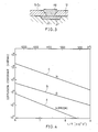
- Fig. 4 is a graph showing the diffusion constant of nitrogen in a silicon monocrystal as a function of temperature.
- the axis of abscissa represents the reciprocal of the absolute temperature T, while the axis of ordinate represents the diffusion constant.
- the line (a) expresses the diffusion constant of nitrogen conventionally believed to be true.
- the diffusion constant of nitrogen along this line (a) is lower by a factor of about 102 than the diffusion constant of oxygen expressed by the line (b).
- the conventional data has led us to a thought that, even if silicon wafers are placed in a nitrogen atmosphere, the wafers would not substantially be diffused with nitrogen into them.
- the present inventors have found from the results of precise experiments conducted by them that the diffusion constant of nitrogen is in fact unexpectedly higher. That is, as indicated by the line (c) which expresses the diffusion constant of nitrogen obtained by the present inventors, the diffusion constant of nitrogen is larger than the conventionally-believed values by a factor of as much as about 105 and is larger than that of oxygen by a factor of about 103.
- one aspect of the present invention provides a method of strengthening a silicon wafer which comprises: subjecting a silicon wafer to heat treatment at a high temperature of 600 to 1300°C in a gas atmosphere consisting of a nitrogen or nitrogen compound gas and an oxygen gas while part or all of the crystal surface is exposed, thereby forming a film of silicon oxide on the surface of the silicon wafer and, simultaneously, doping the silicon wafer with nitrogen through the film of silicon oxide.
- Another aspect of the present invention provides a method of strengthening a silicon wafer which comprises: subjecting a silicon wafer already having a film of silicon oxide formed on the surface thereof to heat treatment at a high temperature of 600 to 1300°C in a gas atmosphere consisting of a nitrogen or nitrogen compound gas, thereby doping the silicon wafer with nitrogen.
- the method in accordance with the present invention provides the following effects. First, since doping with nitrogen is effected in the state of a silicon wafer, the crystal is naturally free from disturbances attributing to growth and, deterioration in crystallinity does not absolutely occur exposing it to the excessive nitrogen in a gas atmosphere at a high temperature to facilitate the sufficient doping.
- the doping can be performed within a short time.
- any defects including slippage and dislocation and the like which may be produced specially around trenched structures or often in the other area of the surface can be locked where they are not to propagate and degrade components in larger area by the action of nitrogen, which in short strengthens the relevant portions of the wafer.
- Fig. 1 illustrates a furnace for doping a silicon wafer with nitrogen.
- a plurality of parallel grooves are formed in the upper surface of a quartz boat 10, and they each receive the lower end portion of a silicon wafer 12.
- the quartz boat 10 with the silicon wafers 12 arranged in this condition is shoved into a nitrogen doping quartz glass tube 14 through an opening thereof provided at the left end, as viewed in Fig. 1. This opening is closed by a cap 16 thereafter.
- the nitrogen doping quartz glass tube 14 is surrounded by a pipe 18 to diminish temperature fluctuations, and an electrical wire 20 which serves as a heater is wound around the outer peripheral surface of the pipe 18.
- An inlet pipe 22 is connected to the right end of the nitrogen doping quartz glass tube 14.
- a flow rate adjusting valve 23 is equipped in the inlet pipe 22 to supply oxygen gas into the nitrogen doping quartz glass tube 14 through them.
- a second inlet pipe 24 branches from the first inlet pipe 22, and a valve 26 is equipped in the second inlet pipe 24 to supply nitrogen gas into the nitrogen doping quartz glass tube 14 through them.
- the oxygen and nitrogen gases will form the atmosphere within the nitrogen doping quartz glass tube 14 and they will be discharged to the outside through an outlet pipe 28 connected to the upper left portion of the tube 14.
- the silicon wafers 12 have each been prepared for use in manufacture of, for instance, a DRAM having a trench capacitor, and they each have on the surface 30 thereof a trench 32 which serves as a three dimensional fine structure, as shown in Fig. 2.
- the trench 32 has been formed by an anisotropic reactive ion etching process employing a patterned silicon oxide mask with an opening which exposes a portion of the underlying surface and a CCl4 gas.
- the diameter and the depth of the trench 32 are, for instance, 2 ⁇ m and 20 ⁇ m, respectively.
- Crystal strain is newly generated after this dry- etching at the corners at the intersection of the surface 30 and the walls of the trench 32 and at the bottom, e.g., at the portion indicated by symbols X.
- crystallographic defects remain as they were in the crystal or will be often generated in the fabrication of integrated circuit devices on the wafer.
- the wafer which is in this condition is subjected to heat treatment at a temperature of about 700 to 1250°C, there is the great risk that the crystal strain and the crystallographic defects may lead to occurrence of various defects or grow further owing to the thermal stress, thereby deteriorating the component produced including the trench or not including it on the surface 30 of the wafer 12.
- Such risk therefore, inevitably limits the increase in the integration density that is possible by making the trench 32 narrower and deeper.
- the heater 20 is turned on to heat the nitrogen doping quartz glass tube 14 to a temperature of about 600 to 1300°C, preferably to a temperature of about 1000°C.
- the flow rate control valve 23 and the valve 26 are opened to supply an oxygen gas and a nitrogen gas, respectively, into the interior of the tube 14.
- the concentration of oxygen in the atmosphere within the nitrogen doping tube 14 is determined depending on the temperature within the tube 14, the period during which the oxygen gas is supplied to the tube 14, and the desired thickness of a SiO2 film on the wall and bottom surface of the trench 32.
- the opening of the flow rate adjusting valve 23 is adjusted to determine oxygen concentration.
- the concentration of nitrogen in the atmosphere within the tube 14 is determined depending on the temperature of the tube 14, the period during which the nitrogen gas is supplied to the tube 14, and the thickness as well as the quality of the SiO2 film.
- the method of the present invention makes the concentration of nitrogen to be limitted by no upper limit.
- the valve 26 is simply opened for supplying nitrogen, and there is no need to use a flow rate adjusting valve for precise control of nitrogen concentration in the atmosphere.
- the flow rate of nitrogen gas varies in accordance with the doping level required, if a furnace of a standard size is used, the flow rate is usually about 1 to 20 l/min, and the period is usually about 1 to 10 minutes.
- a SiO2 film is formed on the wall and bottom surface of the trench 32 of a silicon wafer 12, while nitrogen penetrates into the silicon wafer through this film and part of the nitrogen is trapped at portions where there are strains and crystallographic defects, for instance, dislocations, thereby hardening these portions against plastic deformation by its locking action. It is considered that nitrogen is trapped and Si3N4 is formed.
- valves 23 and 26 should be operated in such a manner that the valve 23 is opened in advance of the opening of the valve 26, so that no Si3N4 film is formed before the formation of the SiO2 film.
- valve closing operation either the valve 26 or the valve 23 may be closed first.
- An N-type silicon wafer 12 has integrated circuit devices formed on the surface thereof. That is, a p+ layer has been formed by thermally diffused boron through a patterned SiO2 mask overlying the silicon wafer 12, and Al is deposited over the mask including an opening in the SiO2 film at a location above the p+ layer.
- the interface of the p+ layer and the deposited Al and the junction of the N-type substrate and the p+ layer are usually stressed and often include a variety of crystallographic defects such as dislocations as typical. The stress and defects tend to develop to defects or grow further respectively during heat treatment. To prevent such problems in the further progress of integrated circuit fabrication, the silicon wafer 12 should be doped with nitrogen.
- This doping is performed in the same manner as that of the first embodiment, except that, in this second embodiment, only a nitrogen gas is supplied to the inside of the nitrogen doping tube 14 since the SiO2 layer is already formed on the surface of the silicon wafer 12. The thus supplied nitrogen disperses around and at the above-mentioned junction or interface.
- the nitrogen gas may be substituted by a nitrogen compound gas such as ammonia.
- the SiO2 film is not limited to a film formed by thermal oxidation, and it may alternatively be an oxide film formed by the CVD method. Needless to say, the SiO2 film may be either a field oxide film or a gate oxide film.
- the silicon wafer can be doped with nitrogen through this film provided that this film is very thin.
Landscapes
- Crystals, And After-Treatments Of Crystals (AREA)
- Formation Of Insulating Films (AREA)
- Semiconductor Memories (AREA)
Applications Claiming Priority (2)
| Application Number | Priority Date | Filing Date | Title |
|---|---|---|---|
| JP73441/87 | 1987-03-27 | ||
| JP62073441A JPS63239200A (ja) | 1987-03-27 | 1987-03-27 | シリコンウエ−ハ強化方法 |
Publications (2)
| Publication Number | Publication Date |
|---|---|
| EP0284107A2 true EP0284107A2 (fr) | 1988-09-28 |
| EP0284107A3 EP0284107A3 (fr) | 1989-10-25 |
Family
ID=13518329
Family Applications (1)
| Application Number | Title | Priority Date | Filing Date |
|---|---|---|---|
| EP88104932A Withdrawn EP0284107A3 (fr) | 1987-03-27 | 1988-03-26 | Méthode pour durcir une plaquette de silicium |
Country Status (2)
| Country | Link |
|---|---|
| EP (1) | EP0284107A3 (fr) |
| JP (1) | JPS63239200A (fr) |
Cited By (3)
| Publication number | Priority date | Publication date | Assignee | Title |
|---|---|---|---|---|
| US5512519A (en) * | 1994-01-22 | 1996-04-30 | Goldstar Electron Co., Ltd. | Method of forming a silicon insulating layer in a semiconductor device |
| DE19941902A1 (de) * | 1999-09-02 | 2001-03-15 | Wacker Siltronic Halbleitermat | Verfahren zur Herstellung von mit Stickstoff dotierten Halbleiterscheiben |
| EP1035236A4 (fr) * | 1998-08-31 | 2007-01-10 | Shinetsu Handotai Kk | Plaquette de silicium monocristallin, plaquette de silicium epitaxiee et leur procede de production |
Families Citing this family (2)
| Publication number | Priority date | Publication date | Assignee | Title |
|---|---|---|---|---|
| KR100942146B1 (ko) | 2007-10-05 | 2010-02-17 | 주식회사 실트론 | 펄스 가스 유동 증착방법, 그 장치 및 이를 이용한에피택셜 웨이퍼의 제작 방법 |
| JP6333182B2 (ja) * | 2015-01-05 | 2018-05-30 | グローバルウェーハズ・ジャパン株式会社 | シリコンウェーハ及びその製造方法 |
Family Cites Families (1)
| Publication number | Priority date | Publication date | Assignee | Title |
|---|---|---|---|---|
| JPS5559729A (en) * | 1978-10-27 | 1980-05-06 | Fujitsu Ltd | Forming method of semiconductor surface insulating film |
-
1987
- 1987-03-27 JP JP62073441A patent/JPS63239200A/ja active Pending
-
1988
- 1988-03-26 EP EP88104932A patent/EP0284107A3/fr not_active Withdrawn
Cited By (4)
| Publication number | Priority date | Publication date | Assignee | Title |
|---|---|---|---|---|
| US5512519A (en) * | 1994-01-22 | 1996-04-30 | Goldstar Electron Co., Ltd. | Method of forming a silicon insulating layer in a semiconductor device |
| EP1035236A4 (fr) * | 1998-08-31 | 2007-01-10 | Shinetsu Handotai Kk | Plaquette de silicium monocristallin, plaquette de silicium epitaxiee et leur procede de production |
| DE19941902A1 (de) * | 1999-09-02 | 2001-03-15 | Wacker Siltronic Halbleitermat | Verfahren zur Herstellung von mit Stickstoff dotierten Halbleiterscheiben |
| US6350314B1 (en) | 1999-09-02 | 2002-02-26 | WACKER SILTRONIC GESELLSCHAFT FüR HALBLEITERMATERIALIEN AG | Process for producing nitrogen-doped semiconductor wafers |
Also Published As
| Publication number | Publication date |
|---|---|
| JPS63239200A (ja) | 1988-10-05 |
| EP0284107A3 (fr) | 1989-10-25 |
Similar Documents
| Publication | Publication Date | Title |
|---|---|---|
| KR100455400B1 (ko) | 아르곤/암모니아 급속 열적 어닐링 공정을 포함한 실리콘웨이퍼의 제조방법 | |
| US8642449B2 (en) | Silicon wafer | |
| US6821344B2 (en) | Czochralski pullers including heat shield housings having sloping top and bottom | |
| KR100378184B1 (ko) | 제어된 결함 분포를 갖는 실리콘 웨이퍼, 그의 제조공정및 단결정 실리콘 잉곳의 제조를 위한 초크랄스키 풀러 | |
| EP2110466B1 (fr) | Procédé de fabrication de silicium monocristallin | |
| JP2004533125A (ja) | イオン注入によるイントリンシックゲッタリングを有するシリコン・オン・インシュレータ構造体を製造する方法 | |
| KR20010031575A (ko) | 실리콘 단결정 웨이퍼, 에피택셜 실리콘 웨이퍼와 그제조방법 | |
| US5951755A (en) | Manufacturing method of semiconductor substrate and inspection method therefor | |
| JP2004503086A (ja) | 削剥領域を備えたシリコンウエハの製造方法及び製造装置 | |
| EP0984486A2 (fr) | Etape de prérecuit/oxidation combinée utilisant un traitement thermique rapide (RTP) | |
| US6238478B1 (en) | Silicon single crystal and process for producing single-crystal silicon thin film | |
| US5574307A (en) | Semiconductor device and method of producing the same | |
| KR100347141B1 (ko) | 에피택셜 실리콘 웨이퍼 제조 방법 | |
| US7229501B2 (en) | Silicon epitaxial wafer and process for manufacturing the same | |
| JPH10144698A (ja) | シリコンウエーハ及びその製造方法 | |
| KR100309462B1 (ko) | 반도체 소자의 웨이퍼 및 그 제조방법 | |
| JPS63239200A (ja) | シリコンウエ−ハ強化方法 | |
| KR100500394B1 (ko) | 에피택셜 실리콘웨이퍼의 제조 방법 | |
| KR100385961B1 (ko) | 제어된 결함 분포를 갖는 실리콘 웨이퍼 및 그의 제조공정 | |
| KR100734615B1 (ko) | N-형 반도체 잉곳 및 그 제조 방법 | |
| JPS6027678A (ja) | 単結晶育成方法 | |
| HK1023226A (en) | Combined preanneal/oxidation step using rapid thermal processing (rtp) |
Legal Events
| Date | Code | Title | Description |
|---|---|---|---|
| PUAI | Public reference made under article 153(3) epc to a published international application that has entered the european phase |
Free format text: ORIGINAL CODE: 0009012 |
|
| AK | Designated contracting states |
Kind code of ref document: A2 Designated state(s): DE FR GB |
|
| PUAL | Search report despatched |
Free format text: ORIGINAL CODE: 0009013 |
|
| AK | Designated contracting states |
Kind code of ref document: A3 Designated state(s): DE FR GB |
|
| STAA | Information on the status of an ep patent application or granted ep patent |
Free format text: STATUS: THE APPLICATION IS DEEMED TO BE WITHDRAWN |
|
| 18D | Application deemed to be withdrawn |
Effective date: 19900426 |