EP0284151B1 - Dispositif d'interface pour connexions électriques dans les machines à laver et à sécher, dispositifs ayant des éléments plans rigides et circuits imprimés flexibles - Google Patents
Dispositif d'interface pour connexions électriques dans les machines à laver et à sécher, dispositifs ayant des éléments plans rigides et circuits imprimés flexibles Download PDFInfo
- Publication number
- EP0284151B1 EP0284151B1 EP88200504A EP88200504A EP0284151B1 EP 0284151 B1 EP0284151 B1 EP 0284151B1 EP 88200504 A EP88200504 A EP 88200504A EP 88200504 A EP88200504 A EP 88200504A EP 0284151 B1 EP0284151 B1 EP 0284151B1
- Authority
- EP
- European Patent Office
- Prior art keywords
- rigid
- plane
- fact
- interface device
- flexible printed
- Prior art date
- Legal status (The legal status is an assumption and is not a legal conclusion. Google has not performed a legal analysis and makes no representation as to the accuracy of the status listed.)
- Expired - Lifetime
Links
- 238000005406 washing Methods 0.000 title description 3
- 238000001035 drying Methods 0.000 title 1
- 238000003780 insertion Methods 0.000 claims description 10
- 230000037431 insertion Effects 0.000 claims description 10
- 238000005476 soldering Methods 0.000 claims description 3
- 238000010276 construction Methods 0.000 description 3
- 238000004519 manufacturing process Methods 0.000 description 2
- 230000010287 polarization Effects 0.000 description 2
- 239000004020 conductor Substances 0.000 description 1
- 238000010586 diagram Methods 0.000 description 1
- 238000009826 distribution Methods 0.000 description 1
- 238000010438 heat treatment Methods 0.000 description 1
- 238000000034 method Methods 0.000 description 1
- 238000009877 rendering Methods 0.000 description 1
Images

Classifications
-
- H—ELECTRICITY
- H01—ELECTRIC ELEMENTS
- H01R—ELECTRICALLY-CONDUCTIVE CONNECTIONS; STRUCTURAL ASSOCIATIONS OF A PLURALITY OF MUTUALLY-INSULATED ELECTRICAL CONNECTING ELEMENTS; COUPLING DEVICES; CURRENT COLLECTORS
- H01R12/00—Structural associations of a plurality of mutually-insulated electrical connecting elements, specially adapted for printed circuits, e.g. printed circuit boards [PCB], flat or ribbon cables, or like generally planar structures, e.g. terminal strips, terminal blocks; Coupling devices specially adapted for printed circuits, flat or ribbon cables, or like generally planar structures; Terminals specially adapted for contact with, or insertion into, printed circuits, flat or ribbon cables, or like generally planar structures
- H01R12/50—Fixed connections
- H01R12/59—Fixed connections for flexible printed circuits, flat or ribbon cables or like structures
- H01R12/62—Fixed connections for flexible printed circuits, flat or ribbon cables or like structures connecting to rigid printed circuits or like structures
-
- H—ELECTRICITY
- H05—ELECTRIC TECHNIQUES NOT OTHERWISE PROVIDED FOR
- H05K—PRINTED CIRCUITS; CASINGS OR CONSTRUCTIONAL DETAILS OF ELECTRIC APPARATUS; MANUFACTURE OF ASSEMBLAGES OF ELECTRICAL COMPONENTS
- H05K1/00—Printed circuits
- H05K1/02—Details
- H05K1/11—Printed elements for providing electric connections to or between printed circuits
- H05K1/118—Printed elements for providing electric connections to or between printed circuits specially for flexible printed circuits, e.g. using folded portions
-
- H—ELECTRICITY
- H05—ELECTRIC TECHNIQUES NOT OTHERWISE PROVIDED FOR
- H05K—PRINTED CIRCUITS; CASINGS OR CONSTRUCTIONAL DETAILS OF ELECTRIC APPARATUS; MANUFACTURE OF ASSEMBLAGES OF ELECTRICAL COMPONENTS
- H05K2201/00—Indexing scheme relating to printed circuits covered by H05K1/00
- H05K2201/04—Assemblies of printed circuits
- H05K2201/042—Stacked spaced PCBs; Planar parts of folded flexible circuits having mounted components in between or spaced from each other
-
- H—ELECTRICITY
- H05—ELECTRIC TECHNIQUES NOT OTHERWISE PROVIDED FOR
- H05K—PRINTED CIRCUITS; CASINGS OR CONSTRUCTIONAL DETAILS OF ELECTRIC APPARATUS; MANUFACTURE OF ASSEMBLAGES OF ELECTRICAL COMPONENTS
- H05K2201/00—Indexing scheme relating to printed circuits covered by H05K1/00
- H05K2201/09—Shape and layout
- H05K2201/09145—Edge details
- H05K2201/09172—Notches between edge pads
-
- H—ELECTRICITY
- H05—ELECTRIC TECHNIQUES NOT OTHERWISE PROVIDED FOR
- H05K—PRINTED CIRCUITS; CASINGS OR CONSTRUCTIONAL DETAILS OF ELECTRIC APPARATUS; MANUFACTURE OF ASSEMBLAGES OF ELECTRICAL COMPONENTS
- H05K2201/00—Indexing scheme relating to printed circuits covered by H05K1/00
- H05K2201/10—Details of components or other objects attached to or integrated in a printed circuit board
- H05K2201/10007—Types of components
- H05K2201/10189—Non-printed connector
-
- H—ELECTRICITY
- H05—ELECTRIC TECHNIQUES NOT OTHERWISE PROVIDED FOR
- H05K—PRINTED CIRCUITS; CASINGS OR CONSTRUCTIONAL DETAILS OF ELECTRIC APPARATUS; MANUFACTURE OF ASSEMBLAGES OF ELECTRICAL COMPONENTS
- H05K2201/00—Indexing scheme relating to printed circuits covered by H05K1/00
- H05K2201/10—Details of components or other objects attached to or integrated in a printed circuit board
- H05K2201/10227—Other objects, e.g. metallic pieces
- H05K2201/10295—Metallic connector elements partly mounted in a hole of the PCB
-
- H—ELECTRICITY
- H05—ELECTRIC TECHNIQUES NOT OTHERWISE PROVIDED FOR
- H05K—PRINTED CIRCUITS; CASINGS OR CONSTRUCTIONAL DETAILS OF ELECTRIC APPARATUS; MANUFACTURE OF ASSEMBLAGES OF ELECTRICAL COMPONENTS
- H05K3/00—Apparatus or processes for manufacturing printed circuits
- H05K3/46—Manufacturing multilayer circuits
- H05K3/4611—Manufacturing multilayer circuits by laminating two or more circuit boards
-
- H—ELECTRICITY
- H05—ELECTRIC TECHNIQUES NOT OTHERWISE PROVIDED FOR
- H05K—PRINTED CIRCUITS; CASINGS OR CONSTRUCTIONAL DETAILS OF ELECTRIC APPARATUS; MANUFACTURE OF ASSEMBLAGES OF ELECTRICAL COMPONENTS
- H05K3/00—Apparatus or processes for manufacturing printed circuits
- H05K3/46—Manufacturing multilayer circuits
- H05K3/4688—Composite multilayer circuits, i.e. comprising insulating layers having different properties
- H05K3/4691—Rigid-flexible multilayer circuits comprising rigid and flexible layers, e.g. having in the bending regions only flexible layers
Definitions
- the subject of the present invention is an electrical interface device especially for the electrical equipment of washing machines and the like.
- control of the cycle sequences of said machines is realised by an electromechanical and/or electronic programmer, to which there are led all the electrical power and control cables of the various electrically operated components, such as: motors, pumps, heating resistors and the like.
- All the aforementioned cables are, at present, connected to the programmer by means of connectors of various types, but singly and without a precise logical order of connection, in that the arrangement of the electrical outputs of the programmer is associated with its internal structure and not with the final operating diagram or layout; furthermore, no distinction is made between power outputs and non-power outputs, which necessitates over-dimensioning of those outputs which, being intended for carrying a current less than five amps, could be constructed in a different manner at a much lesser cost.
- certain types of centralized units applied in the automobile industry are known, but these are not ideal in so far as the internal cabling of the various contact points, the sizes, the weight and the production costs, are concerned.
- FR-A-2 557 378 discloses an interface device where circuit boards having contact teeth are sandwiched on a programming unit, thereby forming contacts and interconnections.
- the objective of the present invention is the overcoming of the aforementioned disadvantages by means of an interface structure particularly for washing machines and the like, which shall be extremely compact, shall reduce to the minimum the number of internal cables necessary, and shall allow the connectors to be arranged in an orderly manner in the sense of affinity of use, at the same time achieving the best orientation possible of the outputs in the direction of the final user device, as well as, when required, the realization of the power outputs in a different manner from that of the non-power outputs.
- said rigid plane shall be a printed circuit of the rigid type and that the flexible printed circuits shall be of a larger size than the rigid plane element.
- the device according to this invention furthermore provides that said rigid plane elements are greater than one in number, and may be disposed below and are disposed above said flexible printed circuits in accordance with a suitable combination of rigid plane elements, rigid printed circuits and supports for power outputs, in such a manner that the rigid elements shall be outside the pack of printed circuits after they have been folded and made electrically and mechanically integral with the programmer and with the flexible printed circuits, which are folded over onto themselves so as to bring the upper rigid elements onto one plane parallel with that of the lower element.
- the mechanical rigidity of the device constructed in this manner is assured by two plane elements, equipped with openings adapted for receiving corresponding projections for fixing, formed on the edges of said rigid elements.
- said alternation of slots and teeth shall be geometrically such as to produce zones for insertion of asymmetrical connectors, achieving a polarization which prevents incorrect insertions on said terminals of the electrical paths, which are arranged and grouped on said teeth on the basis of their final functional or practical affinity; such arrangement and grouping may also be achieved on the basis of closer proximity of the insertion zone for the electrical connectors to the destination component for the signals.
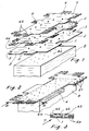
- the device is constituted of a plane rigid element 1, the perimeter of which is shaped to possess projections 2, located between slots 3, forming the insertion zone for the connector 4 (fig. 2); on the upper face of said rigid element 1, there are firmly attached by a known technique one or more printed circuits of the flexible type 5, the edge of which is shaped in such a manner that the zones in which the electrical connection strips 6 are formed coincide, although on different planes, with the corresponding zones 2 of the rigid element 1.
- connection zone 7 in which the different contact strips 6a and 6b can be selected from among those that are alike, for example for function or for destination of use (such as all the controls of the pump).
- Said alternation of projections 2 and slots 3 is, moreover, adapted for making the connection zones 7 asymmetrical among themselves, thereby achieving a polarization, as a result of which it is possible to avoid the frequent errors of insertion of the single connectors.
- the interface device constructed in this manner is then applied to the programmer according to the desired arrangement of the holes and of the needles 8a of said programmer and, after this, by flow soldering, made possible by the fact that all the components, including the power outputs 21 appropriately pointing downards, again lie on a single plane, electrically and mechanically connected to it.
- the interface device by realizing the rigid plane 1 of a printed circuit of the rigid type, which assures simultaneously the mechanical rigidity and the presence of further electrical paths.
- fig. 4 One possible variant is illustrated in fig. 4, in which it is shown that there are applied, to said rigid plane element 1, the flexible printed circuits which may have a larger dimension than that of the rigid plane 1; in this manner, two rigid elements, selected according to the requirements, mays be welded onto the free end projecting flexible circuit portions 9a, 9b, 9c; in the example of this figure, a rigid printed circuit 10 and a support for power outputs 11.
- the rigid elements 1, 10 and 11 can be preselected in accordance with a suitable combination of rigid plane, rigid printed circuit and support for power outputs.
- the supporting structure thus formed is adapted for withstanding, under operating conditions, the loads and/or pressures resulting from the insertion and removal of the female connectors without the possibility of accidental contacts taking place between the facing contact points.
- the application of the interface device to the electromechanical and/ or electronic components as described also enables the or some of the male connectors to be grouped in such a manner as to permit the separate construction of the associated cabling with female terminal connectors already fitted, in such a way as to reduce production costs and to eliminate the possibility of mistakes in connecting up the component with the various items of equipment controlled or operated by it.
Landscapes
- Engineering & Computer Science (AREA)
- Microelectronics & Electronic Packaging (AREA)
- Combinations Of Printed Boards (AREA)
- Coupling Device And Connection With Printed Circuit (AREA)
- Structure Of Printed Boards (AREA)
Claims (4)
- Dispositif d'interface électrique pour composants électromécaniques de programmation (8) comprenant au moins un élément plan rigide de base (1) présentant des bords profilés avec une alternance de fentes (3) et de dents (2), élément plan (1) auquel sont fermement appliqués un ou plusieurs circuits imprimés souples (5), reliés électriquement l'un à l'autre et pouvant être reliés aux composants électromécaniques de programmation (8), les bornes (6a, 6b) des trajets électriques des circuits souples (5) étant amenées auxdites dents (2), caractérisé par le fait qu'il comprend au moins un élément rigide supplémentaire (10, 11) solidaire de manière électrique et mécanique d'une extrémité (9a) du circuit imprimé souple (5) et pouvant être disposé dans un plan parallèle et au-dessus de l'élément rigide de base (1) par pliage des circuits souples (5), deux éléments plans (13a, 13b) étant prévus pour la rigidité mécanique du dispositif d'interface ; et par le fait que des sorties (21), appropriées à l'insertion de connecteurs de puissance, sont montées sur l'élément plan rigide de base (1), en réalisant de cette manière un dispositif d'interface ayant des zones adaptées à l'insertion de connecteurs électriques, qu'ils soient de puissance faible ou de puissance élevée.
- Dispositif selon la revendication 1, caractérisé par le fait que ledit élément plan rigide de base (1) est un circuit imprimé de type rigide qui présente, à son extrémité libre, des zones qui sont rendues conductrices et adaptées à être directement reliées au dispositif d'un utilisateur.
- Dispositif selon la revendication 1. caractérisé par le fait que lesdits deux éléments plans (13a, 13b) sont équipés de fenêtres (13c) adaptées à recevoir des saillies de fixation correspondantes (14) formées sur les bords desdits éléments rigides (1, 10, 11), auxquels ils sont reliés selon une direction orthogonale à l'élément de base (1).
- Dispositif selon la revendication 1, caractérisé par le fait que lesdites sorties (21) pour l'insertion des connecteurs de puissance sont orientées vers le côté de liaison avec les composants de programmation (8) pour permettre, par écoulement, la soudure du dispositif aux composants de programmation.
Applications Claiming Priority (2)
| Application Number | Priority Date | Filing Date | Title |
|---|---|---|---|
| IT19807/87A IT1202670B (it) | 1987-03-23 | 1987-03-23 | Dispositivo di interfaccia per connessioni elettriche in macchine lavatrici e asciugatrici ad elementi piani rigidi e circuiti stampati flessibili |
| IT1980787 | 1987-03-23 |
Publications (3)
| Publication Number | Publication Date |
|---|---|
| EP0284151A2 EP0284151A2 (fr) | 1988-09-28 |
| EP0284151A3 EP0284151A3 (en) | 1990-02-07 |
| EP0284151B1 true EP0284151B1 (fr) | 1994-10-05 |
Family
ID=11161437
Family Applications (1)
| Application Number | Title | Priority Date | Filing Date |
|---|---|---|---|
| EP88200504A Expired - Lifetime EP0284151B1 (fr) | 1987-03-23 | 1988-03-18 | Dispositif d'interface pour connexions électriques dans les machines à laver et à sécher, dispositifs ayant des éléments plans rigides et circuits imprimés flexibles |
Country Status (5)
| Country | Link |
|---|---|
| US (1) | US4895524A (fr) |
| EP (1) | EP0284151B1 (fr) |
| DE (1) | DE3851712T2 (fr) |
| ES (1) | ES2060641T3 (fr) |
| IT (1) | IT1202670B (fr) |
Families Citing this family (9)
| Publication number | Priority date | Publication date | Assignee | Title |
|---|---|---|---|---|
| IT1228333B (it) * | 1989-02-09 | 1991-06-11 | Crouzet Spa | Procedimento per la realizzazione e l'applicazione di interfaccia a piastra per il collegamento elettrico in apparecchiature di comando e controllo con terminali di connessione a lamina o simile e relativa apparecchiatura con interfaccia a piastra per il collegamento elettrico. |
| FR2644939B1 (fr) * | 1989-03-22 | 1991-05-24 | Eaton Controls Sa | Languette de connexion electrique pour circuit imprime, ensemble de connexion comprenant de telles languettes, et procede de realisation de cet ensemble |
| DE3932860A1 (de) * | 1989-10-02 | 1991-04-11 | Thomson Brandt Gmbh | Spulenanordnung |
| US5276590A (en) * | 1991-10-24 | 1994-01-04 | International Business Machines Corporation | Flex circuit electronic cards |
| US5573172A (en) * | 1993-11-08 | 1996-11-12 | Sawtek, Inc. | Surface mount stress relief hidden lead package device and method |
| US5369551A (en) * | 1993-11-08 | 1994-11-29 | Sawtek, Inc. | Surface mount stress relief interface system and method |
| US5579204A (en) * | 1994-08-05 | 1996-11-26 | Emc Corporation | Disk carrier assembly |
| JP2002058132A (ja) * | 2000-08-08 | 2002-02-22 | Sumitomo Wiring Syst Ltd | 電気接続箱 |
| WO2014190240A1 (fr) * | 2013-05-23 | 2014-11-27 | Rapid Diagnostek | Dispositif d'interconnexion et module l'utilisant |
Family Cites Families (10)
| Publication number | Priority date | Publication date | Assignee | Title |
|---|---|---|---|---|
| US3319216A (en) * | 1965-03-25 | 1967-05-09 | Fischer & Porter Co | Connector for flat cables |
| US3710197A (en) * | 1971-02-11 | 1973-01-09 | Westinghouse Electric Corp | Power interlock for electronic circuit cards |
| US3723635A (en) * | 1971-08-16 | 1973-03-27 | Western Electric Co | Double-sided flexible circuit assembly and method of manufacture therefor |
| US3848209A (en) * | 1974-01-02 | 1974-11-12 | Honeywell Inf Systems | Magnetic field coil assembly for a magnetic bubble domain device |
| ATA25474A (de) * | 1974-01-14 | 1977-03-15 | Kopera Adalbert | Schaltungsanordnung |
| DE2517767A1 (de) * | 1975-04-18 | 1976-10-21 | Bosch Siemens Hausgeraete | Haushaltgeraet, wie waschautomat, geschirrspueler, kuehlschrank oder dergleichen |
| US3971127A (en) * | 1975-09-10 | 1976-07-27 | Bell Telephone Laboratories, Incorporated | Method of fabricating a printed wiring board assembly |
| JPS57193094A (en) * | 1981-05-18 | 1982-11-27 | Matsushita Electric Industrial Co Ltd | Electronic circuit part and method of mounting same |
| DE3346493C2 (de) * | 1983-12-22 | 1986-09-04 | Bosch-Siemens Hausgeräte GmbH, 7000 Stuttgart | Vorrichtung zum Verbinden von elektrischen Anschlüssen |
| JPS61151386U (fr) * | 1985-03-12 | 1986-09-18 |
-
1987
- 1987-03-23 IT IT19807/87A patent/IT1202670B/it active
-
1988
- 1988-03-18 ES ES88200504T patent/ES2060641T3/es not_active Expired - Lifetime
- 1988-03-18 DE DE3851712T patent/DE3851712T2/de not_active Expired - Fee Related
- 1988-03-18 EP EP88200504A patent/EP0284151B1/fr not_active Expired - Lifetime
- 1988-03-21 US US07/171,474 patent/US4895524A/en not_active Expired - Fee Related
Also Published As
| Publication number | Publication date |
|---|---|
| DE3851712D1 (de) | 1994-11-10 |
| ES2060641T3 (es) | 1994-12-01 |
| EP0284151A2 (fr) | 1988-09-28 |
| US4895524A (en) | 1990-01-23 |
| IT1202670B (it) | 1989-02-09 |
| EP0284151A3 (en) | 1990-02-07 |
| IT8719807A0 (it) | 1987-03-23 |
| DE3851712T2 (de) | 1995-05-24 |
Similar Documents
| Publication | Publication Date | Title |
|---|---|---|
| US5158471A (en) | Power connector with current distribution | |
| EP0240453B1 (fr) | Boîte de jonction programmable | |
| US3033914A (en) | Printed circuit boards | |
| US5847345A (en) | Push button electrical switch | |
| US6007350A (en) | Electrical connection box | |
| US3624587A (en) | Clinched-wire interconnection device for printed circuit boards | |
| AU2019308280A1 (en) | Improved outlet connection schema for a PDU | |
| EP0284151B1 (fr) | Dispositif d'interface pour connexions électriques dans les machines à laver et à sécher, dispositifs ayant des éléments plans rigides et circuits imprimés flexibles | |
| US5040996A (en) | Central circuit arrangement for motor vehicles | |
| EP1487054B1 (fr) | Structure de connexion pour circuit électrique avec élément terminal | |
| CA1202055A (fr) | Module de branchement sur reseau en c.a. | |
| EP0039175A2 (fr) | Assemblage de connecteurs électriques pour des plaquettes à circuits imprimés | |
| JPS62211941A (ja) | 電力供給用間插板構造体 | |
| US3523268A (en) | Relay mounting socket with printed circuit board | |
| US3745510A (en) | Printed circuit board/integrated circuit socket combination | |
| US4949222A (en) | Electrical apparatus combination | |
| US7212089B2 (en) | Relay unit and electrical junction box | |
| US5052935A (en) | Prewired circuit module | |
| CN113301757B (zh) | 一种电动车控制器及电动车 | |
| GB2165103A (en) | Multi-terminal connectors | |
| CN211238604U (zh) | 接线座及接线装置 | |
| JPH0355254Y2 (fr) | ||
| GB2263588A (en) | Junction box and bridging terminal | |
| US4059773A (en) | Switch controlled power receptacle system | |
| EP0634889B1 (fr) | Dispositif pour l'introduction et le support de composants électriques |
Legal Events
| Date | Code | Title | Description |
|---|---|---|---|
| PUAI | Public reference made under article 153(3) epc to a published international application that has entered the european phase |
Free format text: ORIGINAL CODE: 0009012 |
|
| AK | Designated contracting states |
Kind code of ref document: A2 Designated state(s): DE ES FR GB IT |
|
| PUAL | Search report despatched |
Free format text: ORIGINAL CODE: 0009013 |
|
| AK | Designated contracting states |
Kind code of ref document: A3 Designated state(s): DE ES FR GB IT |
|
| 17P | Request for examination filed |
Effective date: 19900727 |
|
| 17Q | First examination report despatched |
Effective date: 19920924 |
|
| GRAA | (expected) grant |
Free format text: ORIGINAL CODE: 0009210 |
|
| AK | Designated contracting states |
Kind code of ref document: B1 Designated state(s): DE ES FR GB IT |
|
| REF | Corresponds to: |
Ref document number: 3851712 Country of ref document: DE Date of ref document: 19941110 |
|
| REG | Reference to a national code |
Ref country code: ES Ref legal event code: FG2A Ref document number: 2060641 Country of ref document: ES Kind code of ref document: T3 |
|
| ET | Fr: translation filed | ||
| ITF | It: translation for a ep patent filed | ||
| PLBE | No opposition filed within time limit |
Free format text: ORIGINAL CODE: 0009261 |
|
| STAA | Information on the status of an ep patent application or granted ep patent |
Free format text: STATUS: NO OPPOSITION FILED WITHIN TIME LIMIT |
|
| 26N | No opposition filed | ||
| PGFP | Annual fee paid to national office [announced via postgrant information from national office to epo] |
Ref country code: GB Payment date: 19970310 Year of fee payment: 10 |
|
| PGFP | Annual fee paid to national office [announced via postgrant information from national office to epo] |
Ref country code: ES Payment date: 19980306 Year of fee payment: 11 |
|
| PG25 | Lapsed in a contracting state [announced via postgrant information from national office to epo] |
Ref country code: GB Free format text: LAPSE BECAUSE OF NON-PAYMENT OF DUE FEES Effective date: 19980318 |
|
| PGFP | Annual fee paid to national office [announced via postgrant information from national office to epo] |
Ref country code: FR Payment date: 19980319 Year of fee payment: 11 |
|
| PGFP | Annual fee paid to national office [announced via postgrant information from national office to epo] |
Ref country code: DE Payment date: 19980515 Year of fee payment: 11 |
|
| GBPC | Gb: european patent ceased through non-payment of renewal fee |
Effective date: 19980318 |
|
| PG25 | Lapsed in a contracting state [announced via postgrant information from national office to epo] |
Ref country code: ES Free format text: THE PATENT HAS BEEN ANNULLED BY A DECISION OF A NATIONAL AUTHORITY Effective date: 19990320 |
|
| PG25 | Lapsed in a contracting state [announced via postgrant information from national office to epo] |
Ref country code: FR Free format text: LAPSE BECAUSE OF NON-PAYMENT OF DUE FEES Effective date: 19991130 |
|
| REG | Reference to a national code |
Ref country code: FR Ref legal event code: ST |
|
| PG25 | Lapsed in a contracting state [announced via postgrant information from national office to epo] |
Ref country code: DE Free format text: LAPSE BECAUSE OF NON-PAYMENT OF DUE FEES Effective date: 20000101 |
|
| REG | Reference to a national code |
Ref country code: ES Ref legal event code: FD2A Effective date: 20010604 |
|
| PG25 | Lapsed in a contracting state [announced via postgrant information from national office to epo] |
Ref country code: IT Free format text: LAPSE BECAUSE OF NON-PAYMENT OF DUE FEES Effective date: 20050318 |