EP0285015A2 - Logische Dioden-FET-Schaltung - Google Patents
Logische Dioden-FET-Schaltung Download PDFInfo
- Publication number
- EP0285015A2 EP0285015A2 EP88104808A EP88104808A EP0285015A2 EP 0285015 A2 EP0285015 A2 EP 0285015A2 EP 88104808 A EP88104808 A EP 88104808A EP 88104808 A EP88104808 A EP 88104808A EP 0285015 A2 EP0285015 A2 EP 0285015A2
- Authority
- EP
- European Patent Office
- Prior art keywords
- field effect
- conductive means
- effect transistor
- diodes
- circuitry according
- Prior art date
- Legal status (The legal status is an assumption and is not a legal conclusion. Google has not performed a legal analysis and makes no representation as to the accuracy of the status listed.)
- Withdrawn
Links
Images
Classifications
-
- H—ELECTRICITY
- H03—ELECTRONIC CIRCUITRY
- H03K—PULSE TECHNIQUE
- H03K19/00—Logic circuits, i.e. having at least two inputs acting on one output; Inverting circuits
- H03K19/02—Logic circuits, i.e. having at least two inputs acting on one output; Inverting circuits using specified components
- H03K19/08—Logic circuits, i.e. having at least two inputs acting on one output; Inverting circuits using specified components using semiconductor devices
- H03K19/094—Logic circuits, i.e. having at least two inputs acting on one output; Inverting circuits using specified components using semiconductor devices using field-effect transistors
- H03K19/0956—Schottky diode FET logic
-
- G—PHYSICS
- G11—INFORMATION STORAGE
- G11C—STATIC STORES
- G11C17/00—Read-only memories programmable only once; Semi-permanent stores, e.g. manually-replaceable information cards
- G11C17/06—Read-only memories programmable only once; Semi-permanent stores, e.g. manually-replaceable information cards using diode elements
-
- H—ELECTRICITY
- H03—ELECTRONIC CIRCUITRY
- H03K—PULSE TECHNIQUE
- H03K19/00—Logic circuits, i.e. having at least two inputs acting on one output; Inverting circuits
- H03K19/02—Logic circuits, i.e. having at least two inputs acting on one output; Inverting circuits using specified components
- H03K19/173—Logic circuits, i.e. having at least two inputs acting on one output; Inverting circuits using specified components using elementary logic circuits as components
- H03K19/177—Logic circuits, i.e. having at least two inputs acting on one output; Inverting circuits using specified components using elementary logic circuits as components arranged in matrix form
- H03K19/17704—Logic circuits, i.e. having at least two inputs acting on one output; Inverting circuits using specified components using elementary logic circuits as components arranged in matrix form the logic functions being realised by the interconnection of rows and columns
- H03K19/17708—Logic circuits, i.e. having at least two inputs acting on one output; Inverting circuits using specified components using elementary logic circuits as components arranged in matrix form the logic functions being realised by the interconnection of rows and columns using an AND matrix followed by an OR matrix, i.e. programmable logic arrays
Definitions
- the invention relates to computer-logic circuitry, and more particularly programmable logic array (PLA) and read-only memory (ROM) circuitry.
- PLA programmable logic array
- ROM read-only memory
- RAMS random access memories
- ROMs read only memory
- logic circuits logic circuits
- GaAs Gallium arsenide
- RAMS random access memory
- PLA random access memory
- ROM read-only memory
- the present invention is a circuit that has the capability of providing both PLA and ROM functions having circuits consisting merely of diodes, FETS, and of course, interconnecting conductors.
- the invention can implement various kinds of GaAs ICs. Also the invention maintains the advantage of GaAs high speed capability by keeping the number of circuit gate delays low.
- the PLA has, from input to output, excluding a buffer, effectively no gate delays.
- the ROM function has, from input address to data out, only two- or three-gate delays, depending on the kind of address, excluding output interface circuitry.
- the output interface or buffer circuitry in either case adds only one gate delay.
- the diodes are utilized to perform OR and AND operations in the invention.
- FETs are used in current sources and sinks, and in driver circuits.
- the OR and AND planes of the PLA function are implemented using Schottky diodes. In the ROM function, these OR and AND operations are implemented throughout the whole ROM for addressing, decoding, reading and multiplexing data.
- the invention may be applicable to any solid state semiconductor technology, including that involving high speed or low power techniques, and to different families of the PLA and ROM, including FPLA, (Functional PLA), PROM, EPROM, etc.
- the invention is suitable with FETs using any type of process including depletion, enhancement, or a combination of depletion and enhancement. If the invention is used with enhancement or a combination of depletion and enhancement field effect transistors, only one power supply and a ground reference are required.
- SDFL Schottkydiode-FET logic
- BFL buffered FET logic
- SCFL source-coupled FET logic
- DCFL direct-coupled FET logic
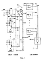
- Figure 1 illustrates an OR/AND plane 380 for the PLA.
- the circuit uses only diodes with the exception of one inverting FET and the pull down and pull up FET's utilized in the current sources and sinks.
- This OR/AND configuration 380 is of great advantage because there is no gate delay in the exclusive diode OR/AND circuit 380. The only gate delay involved is the inverter comprising FETs 396 and 398.
- Circuit 372 of Figure 1 performs an OR function. A high logic signal is put into input 400 forward biasing diode 382 and diode 388 thereby presenting a high signal on line 406 less only the voltage drops of diodes 382 and 388. The signal remains high on line 406 even though inputs into diodes 384 and 386 are low.
- Line 406 is then kept to a low logic state by a current sink incorporating FET 402 having its drain connected to the cathode of diode 390 and its gate and source connected to a negative voltage potential -V SS .
- the anode of diode 390 is connected to a constant current source composed of FET 404 having its drain connected to a ground or a voltage potential V D . (Ground is used in Fig.
- the signal on line 408 goes to the gate of FET 396.
- the drain of FET 396 is connected to a constant current source composed of FET 398 and positive voltage potential V DD .
- the source of FET 396 is connected to ground.
- FET 396 is a switching transistor which transforms the signal on line 408 to inverted signal on output 410. Because of the inversion of the AND signal on line 408 by FET 396, circuit 378 is a NAND logic circuit.
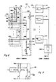
- Circuit 412 in Figure 2 illustrates an AND/OR plane which can be used in the PLA.
- Circuits 414, 416 and 418 are AND logic circuits. For instance in AND circuit 414, if a high logic level input is on 422 and a low logic input is coming into the cathodes of diodes 426 through 428, the output line 432 will be in a low logic state. Current flowing from the constant current source composed of FET 430 and positive voltage potential V DD , through forward-biased diodes 426 through 428 to the low inputs of circuit 414 keep the voltage level of line 432 at a low. If all inputs to circuit 414 are high except for one, the current will flow through the one diode to the low input of circuit 414.
- circuit 414 if all the inputs to circuit 414 are high, line 432 will be high because no current will be flowing from the constant current source. incorporating FET 430. Current will be along line 432 through diode 434 along line 448 through diode 440 to a current sink made up of FET 444 and a negative voltage potential -V SS . Under this condition, line 432 is pulled up by FET 430 to a high state thus resulting in an AND output indicating a high logic state of all of the inputs of circuit 414. AND circuits 416 through 418 function like circuit 414. Circuit 420 of Figure 2 is a NOR logic circuit.
- line 448 is high because the reverse biased diodes 436 through 438 have no effect on the high signal coming from the forward-biased diode 434.
- the only way that line 448 can be low is for all the inputs of circuit 420 to diodes 434, 436 through 438 to be low.
- Line 448 is then pulled down a low state due to a pull-down FET 444 which is connected to a negative voltage potential -V SS composing a current sink. Any current on line 448 goes through diode 440.
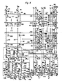
- FIG. 3 is a schematic diagram of the ROM configuration, which is uniquely designed having as active circuit components exclusively diodes and FETs. This specific embodiment has Schottky diodes and metal semiconductor FET's making this configuration adaptable to GaAs integrated circuits.
- the ROM configuration incorporates the above-described diode OR and AND circuits. Data are stored in this ROM configuration in a left data field 26 and a right data field 38. The individual data are stored at the intersections of bit lines 22, 24, 34 and 36 and word line 32. whether the datum is a logic value zero or one is determined at each intersection of a bit line and a word line by a diode connection or no diode connection. In the instance of a bit line and a word line connected by a diode, the stored value is a logic value zero, and in the instance of a bit line and word line not connected by a diode, the stored value is a logic value one.
- bit line 22 and word line 32 intersect in the left data field 26 and the value stored is a zero.
- the value stored at the intersection of bit line 24 and word line 32 is a one since it is not connected by diode 30.
- the intersection of bit line 34 and word line 32 represents a value of one since the lines are not connected by diode 40 and the intersection of lines 36 and 38 represents a logic value zero since the lines are connected by diode 42.
- bit lines represented in Figure 3 in the left data field 26 and the right data field 38 is merely an example of bit lines.
- bit lines there are 160 bit lines in data field 26 and 160 bit lines in data field 38.
- the actual ROM configuration has 512 word lines which extend into the left data field 26 and the right data field 38.
- each data field contains 512 words which are 160 bits long. This results in a 81,920 bit ROM.
- a request for data from the ROM configuration begins with an address to address decoder drivers 44 and 46.
- Address decoder drivers 44 ultimately select the specific word line which contains the data in the left data field 26 and the right data field 38 to be read out. Since there are 512 word lines, each address input to inputs 48 and 50 must be unique enough in order to address one specific word line. Inputs 48 and 50 are merely representative. Utilizing a binary address of logic values one and zero and various combinations of it into address decoder drivers 44, at least nine inputs would be required for individually addressing 512 word lines via the address decoder drivers 44. The additional inputs would have the same circuitry as inputs 48 and 50.
- a high or one logic signal is input to terminal 48 and a low or zero logic signal is input to terminal 50.
- the one logic signal consists of a positive voltage potential and the zero logic signal consists of a zero voltage potential.
- the logic value one input to terminal 48 goes through three voltage level shift diodes 52, from anode to cathode, in series. The diodes 52 adjust the voltage level for the circuitry of the address decoder driver 44.
- the third diode 52 has its cathode connected to the drain of FET 56.
- FET 56 has its gate and source connected to a minus voltage source -V SS .
- FET 56 and voltage source -V SS constitute a current sink.
- the voltage level diode 52 and FET 56 are connected to an address line 58.
- Line 58 goes up to word line driver decoder 60 for word line driver 104 which selects word line 32.
- word line driver decoder 60 There are 511 other decoders like decoder 60 for selecting the other 511 word lines.
- Address line 58 enters all of the word line driver decoders. In this particular case, address line 58 is carrying a logic one value, i.e., a positive voltage to word line driver decoder 60.
- FET 64 functions as a switching transistor and a signal inverter. The source of FET 64 is connected to a zero voltage potential, i.e., ground.
- the drain of FET 64 is connected to the gate and source of FET 66 at node 68.
- the drain of FET 66 is connected to a positive voltage potential V DD .
- FET 66 in combination with positive voltage potential V DD , constitutes a constant current source at node 68.
- the signal input at input 48 becomes inverted at node 68.
- the signal from input 48 to node 68 incurs a one gate delay in FET 64.
- the inverted signal at node 68 goes on through two voltage level shift diodes 72 connected in series, and on to address line 74.
- Address line 74 is connected to the cathode of diode 72 and to the drain of a FET 70.
- the gate and the source of FET 70 are connected to a zero voltage potential, i.e., ground.
- FET's 56, 66 and 70 are active loads at their respective places in the circuit of the address decoder driver 44 corresponding to input 48.
- the zerologic signal or low voltage signal on address line 74 goes to all the other word line driver decoders in addition to word line driver decoder 60.
- the second address signal to address decoder drivers 44 is a low or zero logic value into input 50.
- the signal goes through three voltage level shift diodes 54 from anode to cathode in series to node 80.
- the drain of a FET 76 is connected to node 80.
- the gate and source of FET 76 are both connected to a negative voltage potential -V SS .
- An address line 78 is connected at node 80 and carries the low signal from input 50 through voltage level shift diodes 54 on up to word line driver decoder 60 and all of the other word line driver decoders of the ROM configuration.
- Connected to line 78 in the vicinity of node 80 is the gate of FET 82 which functions as a switching transistor and an inverter of the signal at node 80.
- the source of FET 82 is connected to a zero voltage potential, i.e., ground.
- the drain of FET 82 is connected to node 84.
- the gate and source of FET 86 are connected to node 84.
- the drain of FET 86 is connected to a positive voltage potential V DD .
- the combination of FET 86 and voltage positive potential V DD constitute a constant current source.
- the low signal at input 50 is a high signal at node 84 with a one gate delay of FET 82. With a low input, FET 82 iseffectively off and node 84 exhibits a high signal due to the pull-up FET 86 and positive voltage potential V DD .
- the high logic signal at node 84 goes through two voltage level shift diodes 88 from anode to cathode to anode to cathode onto address line 92.
- the high logic signal on address line 92 goes onto word line driver decoder 60 and all other word line driver decoders in the ROM configuration.
- a FET 90 in the address decoder driver 44. corresponding to input 50, has its drain connected to address line 92 and the cathode of voltage level shift diode 88.
- the gate and the source of FET 90 are both connected to zero potential, i.e., ground.
- FET's 76, 86 and 90 function as active loads in the address decoder driver circuit 44.
- the word line driver decoder 60 of Figure 3 is illustrated in terms of operation.
- the address signal at input 48 of address decoder driver 44 is represented on line 58 as the same signal and the complement of that input signal at input 48 is represented on address line 74.
- the address signal into input 50 of address decoder driver 44 is represented as the same signal on address line 78 and its complement is represented on address line 92.
- the address signals into inputs 48 and 50 of address decoder drivers 44 are a logic high and a logic low, respectively, i.e., a logic one and a logic zero.
- This address is represented on lines 58, 74, 78 and 92, as a high, low, low, and high. respectively.
- These signals on the lines are indicated in Figure 3 by the letters "H” and "L” for high and low signals, respectively.
- Address lines 58, 74. 78 and 92 form intersections with word line driver decode line 102. Of the complementary pair of address lines 58 and 74, only one is connected to the word line driver decode line 102 with a diode 94 or 96. The complementary address lines 78 and 92 intersect the word line driver decode line 102. Only one of the complementary address lines 78 and 92 is connected to word line driver decode line 102 by a diode 98 or a diode 100. Diodes 94, 96, 98 and 100 are decode diodes.
- decode diode 94 is connected with its cathode to line 58 and its anode to word line decode line 102.
- Decode diode 96 is left disconnected with respect to address line 74. Whatever the state of address line 74 is, it does not affect word line driver decoder 60 for driver 104, since there is no connection between the two.
- the other part of the address coming into address decoder drivers 44 is a low at input 50.
- a low at input 50 results in a low on address line 78. Since decode diode 98 is disconnected from line 78 and word line driver decode line 102, address line 78 has no effect on the 'word line driver decoder 60 for driver 32.
- the low signal at the input of 50 goes through voltage level shift diodes 54 to node 80. Because the signal is low at node 80 and the gate of FET 82 is, in effect, turned off. Thus, node 84 and the drain of FET 82 are high due to the pull-up FET 86 which is tied to the positive voltage V DD .
- the high signal goes through the two voltage level shift diodes 88 and up onto address line 92. A high signal is seen by the word line driver decoder 60 for word line driver 32.
- the signal on address line 92 does affect word line driver decode line 102 since decode diode 100 connects lines 92 and 102.
- the address decoder driver circuit 44 and 46 may not be needed if the addresses coming into the ROM 12 include both the true and complement logic levels. This approach would eliminate one gate delay in ROM 12.
- SCFL source-coupled FET logic
- Address lines 58 and 92 are hooked up to line 102 in a logic AND configuration. That means for line 102 to be high both lines 58 and 92 must be high. Assume line 92 to be low. Then the high voltage on line 102 causes current to conduct through diode 100 and line 102 becomes low with the exception of a small voltage drop across diode 100. The same applies when line 58 is low and line 92 is high; line 58 pulls down line 102 through conduction of diode 94. Thus, both lines 58 and 92 must be high for line 102 to be high. For this state to be accomplished, then the address into inputs 48 and 50 of address decoder drivers 44 must be a high and a low, correspondingly.
- line decoder 60 can select word line 32. With the appropriate address. the decoder 60causes line 102 to go from a low to a high state, that in turn raises the voltage from a low to a high state at node 106 in a driver 104.
- a pull-up FET 108 has its drain connected to ground and its gate and source connected to the line which is part of node 106. FET 108 pulls-up line 102.
- FET 112 is a pull-up transistor which has its drain connected to a positive voltage potential V DD .
- FET 112 has its gate and source connected to word line 32, which hold the voltage on word line 32 at a high when FET 110 is off.
- Word line 32 being at a low voltage state, indicates that a data selection is being made from data fields 26 and 38. All bit lines are at a high state when not selected. When word line 32 is at a low state, an indication of selection, then diode 28 indicating a zero state of logic value at that memory cell turns on. Current flows through diode 28 from bit line 22 to word line 32 thereby changing the state of bit line 22 from a high logic value to a low logic value. The unconnected diode 30 indicates a high or one logic value.
- the data for word line 32 is noted on bit lines 22 and 24 as zero and one logic values, respectively. Also, the bit lines 34 and 36 of data field 38 are selected by word line 32.
- the memory cell diode 40 is unconnected indicating a one logic value and the memory cell diode 42 is connected indicating a zero logic value.
- the low state of the selector word line 32 pulls down the bit line 36, thus giving an indication of zero logic value.
- word line 32 or any other word line is not selected, the normal state of the bit lines is high.
- FET's 114 and 116 are pull-up transistors for bit lines 22 and 24. FET's 114 and 116, respectively, have their drains connected to a positive voltage potential V DD . The gates and sources of FET's 114 and 116 are connected to bit lines 22 and 24, respectively. FET's 118 and 120 are pull-up transistors for bit lines 34 and 36, respectively, keeping them in a high state under a nonselection state. FET's 118 and 120 have drains connected to a positive voltage potential V DD . The gates and sources of FET's 118 and 120 are connected to bit lines 34 and 36, respectively.Word line 122 is in a nonselected state or at a high or one logic value.
- Memory cell diodes 124, 126, 128 and 130 have significance as to the data stored in those places when word line 122 is selected, i.e., at a low state. If selected, only then do diodes 124 and 128 turn on, putting bit lines 22 and 34 to a low state, indicating a zero logic value. Diodes 126 and 130 are not functional due to their being unconnected, letting bit lines remain at a high state, indicating a one logic value. It may be noted that the address which selects either word line 32 or word line 122 is unique and therefore only one word line can be selected at a time.
- Data from data fields 26 and 38 coming down bit lines 22, 24, 34 and 36 are joined together in an OR function in the order of bit lines of the respective data fields 26 and 38.
- the datum on bit line 22 goes through OR diode 132 and the datum on bit line 34 goes through OR diode 136 and along line 140 to node 144 where it meets with the datum of bit line 22.
- the datum from bit line 24 goes through OR diode 134 out onto node 146 and the datum from bit line 36 goes on through OR diode 138, along line 142, onto node 146.
- the data at nodes 144 and 146 go through diodes 148 and 150, respectively.
- the information for both pairs of bit lines is OR-ed.
- Data field or memory array selector driver 46 may also be referred to as an address decoder driver 46 being grouped together with address decoder drivers 44 since a signal to the input 152 is a part of the address incorporating inputs 48, 50, and so on.
- a high or one logic value signal at input 152 selects data field 26 and a low or zero logic input into input 152 of driver 46 selects data field 38. For instance, a high signal, put into input 152, goes through three voltage level shifting diodes 154 which are connected in series in the direction of anode to cathode with the signal entering the anode side of the diodes.
- the data field or memory array selector signal next arrives at node 158 which is connected to the drain of pull-down FET 156.
- FET 156 has its source and drain connected to a negative voltage potential -V SS .
- the signal at 158 goes down data field address line 168 as a high or one logic signal.
- the signal on node 158 also goes to the gate of a switching FET 160.
- FET 160 has its source connected to a ground or zero voltage potential.
- the drain of FET 160 is connected to node 172.
- a pull-up FET 162 has a drain connected to a positive voltage potential V DD .
- FET 162 has a gate and source connected to node 172.
- FET 160 Since the signal at gate of FET 160 is high, FET 160 is turned on and node 172 is at approximately a ground potential or a low or zero logic value. This low signal goes on through two voltage level shifting diodes 164 which are connected in series cathode to anode with the signal going through the diodes from anode to cathode out on to data field address line 170.
- the drain of FET 166 is connected to the output of driver 46 which is connected to data field address line 170.
- the gate and source of FET 166 is connected to a zero voltage potential, i.e., ground.
- the low signal on line 170 goes to diode 174 causing field select decode 174 to turn on and to pull field select driver decode line 178 to a low state.
- Decode diode 176 is disconnected since one has a choice of selecting a high signal from 168 or a low signal from 170 for a given high logic value at input 152 of driver 46 since lines 168 and 170 are complementary lines.
- the low signal on line 178 is seen on node 182 of field select line driver 180.
- a pull-up FET 184 has a drain connected to a ground and its gate and source connected to node 182. The low signal on node 182 goes into a gate of a switching FET 186.
- Switching FET 186 has a source connected to a zero voltage potential, i.e., ground, and a drain connected to field select line 190. Connected to field select line 190 is a source and a gate of a pull-up FET 188. FET 188 has its drain connected to a positive voltage potential V DD . Since the low signal shuts off FET 186 the potential on field select line 190 is high due to the pull-up FET 188.
- Field select line 190 is connected to cathodes of field select diodes 194 and 196 in field selector 192.
- the anode of field select diode 194 connected to data bit line 22 and the anode of field select diode 196 is connected to bit line 24.
- bit lines 22 and 24 may be either high or low because if bit line 22 or 24 is low, diodes 194 and 196 are back-biased and thus have no effect on the signals on bit lines 22 and 24.
- diodes 194 and 196 are forward-biased and thus hold bit lines 22 and 24 down to a low signal, preventing the exhibition or reading out of data on bit lines 22 through 24, i.e., data field 26, of any selected word line, viz., 32 or 102.
- a low signal on field select line 190 corresponds to a low signal on input 152 of driver 46. Assume. as indicated in Figure 3, that a high signal "H" is on input 152 of driver 46, thus resulting in a high on field select line 190 thereby allowing data to read out of data field 26. One may look at the effect of the output of driver 46 on data field 38. Having a high on input 152 results in a high logic signal on data field address line 168. Line 168 is connected to field select driver decode line 200 through a field select decode diode 202 having its cathode connected to data address line 168 and its anode connected to field select driver decode line 200.
- diode 202 Since line 200 is normally high due to a pull-up FET 206, diode 202 has a significant effect only when line 168 is a low therefore forward-biasing the diode and pulling line 200 down to a low. That happens only if a low is at input 152 of driver 46.
- the gate and source of FET 206 are connected to node 204 which, in turn, is connected to line 200.
- the drain of FET 206 is connected to a ground.
- the high signal of field select driver decode line 200 goes into field select line driver 228 onto a gate of a switching FET 208.
- FET 208 has a source connected to ground and a drain connected to field select line 210.
- Field select line 210 is connected to a gate and source of a pull-up FET 212.
- the drain of FET 212 is connected to a positive voltage potential V DD . Pull-up FET 212 causes field select line 210 to be normally high.
- field select line 210 has no effect on data field 26 since field select diodes 218 and 222 are not connected between line 210 and bit lines 22 and 24. However, field select line 210 is connected to bit lines 34 and 36 of data field 38 through field select diodes 214 and 216 in field selector 210. Diodes 214 and 216 have cathodes connected to field select line 210 and anodes connected to data bit lines 34 and 36, respectively.
- data bit line 34 or 36 is supposed to be high it is brought down to a low signal if field select line 210 is low due to the forward-biasing of diodes 214 and 216. Since field select diodes 214, 216 and other diodes correspondingly connected to all the data bit lines of data field 38, cause all of the bit lines to be low, then no data can effectively be read out of data field 38.
- Field select diodes 224 and 226 are present in case an alternative connection is desired in lieu of diodes 214 and 216 to the bit lines 34 and 36 respectively of data field 38. Overall, it can be noted that if there is a high signal on input 152 of driver 46 data field 26 is selected and data field 38 is precluded from exhibiting data.
- the byte size of data read is equal to the number of bit lines in either the left or right data field array.
- the byte size can be reduced by adding more sets of field selectors like those of 220 and 192 along with associated lines and drivers.
- Circuit 250 contains OR junctions of corresponding bit lines of the field arrays 26 and 38.
- the OR function is described above in conjunction with Figures 1 and 2.
- the output of the respective selected bit lines 22 and 24, or 34 and 36, are fed through diodes 148 and 150, respectively, onto lines 234 and 236.
- FET's 230 and 232 have their gates and sources connected to a negative voltage potential -V SS .
- the drain of FET 230 is connected to the cathode of diode 148 and to line 234.
- FET 232 has a drain connected to the cathode of diode 150 and to line 236.
- the bit line signal on line 234 goes on to the gate of a switching FET 238.
- the signal on bit line 22 is low and goes through diodes 132 and 148 on to line 234 to the gate of FET 238, thus turning off FET 238.
- the drain of FET 238 is connected to a zero voltage potential, i.e., ground, and the source is connected to an output terminal 246 of circuit 250. Also connected to the source of FET 238 are the gate and source of FET 242.
- the drain of FET 242 is connected to a positive voltage potential V DD . Since FET 238 is turned off by the low signal of bit line 22, the output 246 exhibits a high signal. Bit line 24 has a high signal which goes through diodes 134 and 150 on to line 236 which is connected to the gate of FET 240. FET 240 has a source connected to ground and a drain connected to an output terminal 248 of circuit 250. Also connected to the drain of FET 240 are a gate and a source of FET 244. FET 244 has a drain connected to a positive voltage potential V DD . The high signal on bit line 24 which goes along line 236, turns on FET 240 thereby causing output 248 to be low.
- the high signal at output 246 from circuit 250 goes into an inverter and buffer circuit 252 through a series of three voltage level shift diodes 254 from anode to cathode onto a drain of a pull-down FET 258.
- FET 258 has a gate and a source connected to a negative voltage potential -V SS .
- the high signal on the drain of FET 258 goes on through diode 264 from cathode to anode and on to the gates of FET 266 and FET 268.
- the sources of FET 266 and FET 268 are connected to a zero voltage potential, i.e., ground.
- the drain of FET 266 is connected to the gates of FET's 270 and 272 and to the source of FET 270.
- the drains of FET's 270 and 272 are connected to a positive voltage potential V DD .
- the drain of FET 268 is connected to the source of FET 272 and to output terminal 278 of inverter and buffer circuit 252.
- the high signal at input 246 of circuit 252 which goes on through the voltage level shift diodes 254 and diode 264 onto the gates of FET's 266 and 268, turns on the latter FET 268 resulting in a low output signal at terminal 278.
- the low signal at terminal 248 going into circuit 252 goes through three voltage level shift diodes 256 from anode to cathode and then onto a drain of FET 260 and a cathode of diode 262.
- the gate and source of FET 260 are connected to a negative voltage potential -V SS .
- the anode of diode 262 is connected to gates of FET's 282 and 284.
- the sources of FET s 282 and 284 are connected to a zero voltage potential, i.e., ground.
- the drain of FET 282 is connected to gates of FET's 274 and 276 and to the source of FET 274.
- the drains of FET's 274 and 276 are connected to a positive voltage potential V DD .
- the drain of FET 284 is connected to the source of FET 276 and to output terminal 280 of circuit 252.
- Data are read out on terminals 278 and 280 if lines 286 and 287 from enable circuit 298 are such that the data signals to the gates of FET's 266, 268, 282 and 284 are not blocked.
- a pull-down FET 290 having a gate and a source connected to a negative voltage potential -V SS and a drain connected to the cathode of diode 292, holds the cathode of diode 292 at a low voltage.
- Current from the source of FET 288 flows through forward-biased diode 292 to FET 290.
- FET 288 has a drain connected to a zero voltage potential, i.e., ground, and a gate and a source connected to lines 286 and 287. Lines 286 and 287 are connected to the gates of FET's 266 and 282.
- FET's 288 and 290 results in a low voltage potential on lines 286 and 287 and presents a low signal at the gates of FET's 266, 268, 282 and 284, thereby blocking data to out terminals 278 and 280 and resulting in high signals on the output terminals 278 and 280.
- a high signal is put into terminal 296 of enable circuit 298.
- the high signal goes from anode to cathode through three voltage level shifting diodes 294 which are connected in series.
- the high signal at the cathode of the third voltage level shifting diode 294 goes on to the drain of FET 290 and the cathode of diode 292.
- the voltage potential at the drain of FET 290 is high enough to back-bias diode 292 so that diode 292 does not conduct current and thereby hold the voltage potential low on lines 286 and 287.
- the signals on lines 286 and 287 may vary freely, being either high or low.
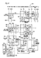
- FIG. 4 Another ROM configuration 300 in Figure 4 has several portions of circuitry which utilize logic which is the obverse of logic utilized in corresponding portions of the ROM configuration 12 described above in Figure 3.
- Configuration 300 of Figure 4 like configuration 12 in Figure 3, uniquely implements diode logic described above in conjunction with Figures 1 and 2.
- a low address signal is entered at input 302 of the word line address driver 306.
- the word line address driver 306 functions similarly as word line address driver 44 in Figure 2.
- the output of the word line address 306 is a low output corresponding to the low input at 302 and a complementary output which is a high, i.e., an inversion of the input.
- the low signal out of word line address driver 306 goes down address line 326 and the inverted output of address driver 306 goes down the address line 328.
- Line 328 is not connected to anything within word line driver 310.
- the low signal going down 326 affects the decode diode 330 which turns on and pulls the word line driver decode line 332 from a normally high state to a low state thereby turning off FET 334 which causes a normally low word line 336 to go to a high state.
- Word line 336 extends into the left half ROM 312 and the right half ROM 314. The high state of word line 336 forward biases a memory cell diode 346 thus raising bit line 338 from a low to a high state. Word line 336 also raises bit line 342 from a low to a high state through the forward-biased memory cell diode 348. The other bit lines intersected by word line 336 but not interconnected with a memory cell diode remain in a low state.
- the data from the bit lines of either the left half ROM 312 or the right half ROM 314 are selected according to a half ROM one at a time. This selection is made with a bit line selector 318 which is driven by the bit line selector driver 316. Selector driver 316 is in turn driven by address driver 308. For instance one may input a high signal to input 304 of address driver 308. Address driver 308 works similarly in function to driver 46 in Figure 3. The high noninverted output of driver 308 goes on down address line 348 which is connected to bit line selector decode line 354 by decode diode 352. Decode diode 352 is not forward-biased because of the normally high state of the bit line selector decode line 354.
- FET 356 is on and the bit line selector driver line 358 is low.
- the low line 358 does not turn on the bit line selector diode 346 since it is backed-biased as it is connected to a high bit line 338.
- Line 358 also has a diode connected to bit line 340. As long as line 358 is low data may pass from the left half ROM 312 on out to the bit line multiplexer and sense amplifier 320.
- the left half ROM 312 and the right half ROM 314 are wiredsuch that, whatever the address signal input at 304 of address driver 308, one half ROM will be in such a state that its data may be read out from its bit lines and the other half ROM will be in such a state that no data may be read out from its bit lines.
- the set of bit lines for the left half ROM 312 and the set of bit lines from right half ROM 314 are fed into a bit line multiplexer and sense amplifier 320. They are connected in an AND configuration and the output of the bit lines of the half ROM being read is inverted and exits at output 364 of the bit line multiplexer and sense amplifier 320.
- word line driver 310 there are only two gate delays from the point of address input at 302 of word line address driver 306 to the output point 364 of the bit line multiplexer and sense amplifier 320.
- the first gate delay is FET 334 in word line driver 310 and the second delay is in FET 366 of bit line multiplexer and sense amplifier 320.
- word line driver 310 is to depend on a signal on address line 328, there is an additional gate delay at the inverting FET 368 in address driver 306.
- the memory data output at terminal 364 may be connected to an inverting buffer 324.
- An additional gate delay results in running the signal through inverting buffer 324.
- Connected to inverting buffer 324 is an enabling circuit 322.
- An enabling signal is fed into input 370 for enabling the ROM configuration 300 at the inverting buffer 324 for the reading out of data.
- Enabling circuit 322 functions similarly to enabling circuit 298 of Figure 3.
- inverting buffer 324 functions like inverting buffer 252 of Figure 3.
Landscapes
- Physics & Mathematics (AREA)
- Mathematical Physics (AREA)
- Engineering & Computer Science (AREA)
- Computer Hardware Design (AREA)
- Computing Systems (AREA)
- General Engineering & Computer Science (AREA)
- Power Engineering (AREA)
- Logic Circuits (AREA)
- Design And Manufacture Of Integrated Circuits (AREA)
- Semiconductor Memories (AREA)
Applications Claiming Priority (2)
| Application Number | Priority Date | Filing Date | Title |
|---|---|---|---|
| US32127 | 1987-03-30 | ||
| US07/032,127 US4845679A (en) | 1987-03-30 | 1987-03-30 | Diode-FET logic circuitry |
Publications (2)
| Publication Number | Publication Date |
|---|---|
| EP0285015A2 true EP0285015A2 (de) | 1988-10-05 |
| EP0285015A3 EP0285015A3 (de) | 1989-07-05 |
Family
ID=21863248
Family Applications (1)
| Application Number | Title | Priority Date | Filing Date |
|---|---|---|---|
| EP88104808A Withdrawn EP0285015A3 (de) | 1987-03-30 | 1988-03-25 | Logische Dioden-FET-Schaltung |
Country Status (3)
| Country | Link |
|---|---|
| US (1) | US4845679A (de) |
| EP (1) | EP0285015A3 (de) |
| JP (1) | JPS641328A (de) |
Cited By (1)
| Publication number | Priority date | Publication date | Assignee | Title |
|---|---|---|---|---|
| EP0394575A1 (de) * | 1988-01-13 | 1990-10-31 | Xilinx, Inc. | Programmierbare logische Vorrichtung |
Families Citing this family (10)
| Publication number | Priority date | Publication date | Assignee | Title |
|---|---|---|---|---|
| US5200924A (en) * | 1989-03-30 | 1993-04-06 | Synergy Semiconductor Corporation | Bit line discharge and sense circuit |
| GB9117680D0 (en) * | 1991-08-16 | 1991-10-02 | Philips Electronic Associated | Electronic matrix array devices |
| US5673218A (en) * | 1996-03-05 | 1997-09-30 | Shepard; Daniel R. | Dual-addressed rectifier storage device |
| US5889694A (en) * | 1996-03-05 | 1999-03-30 | Shepard; Daniel R. | Dual-addressed rectifier storage device |
| US6956757B2 (en) * | 2000-06-22 | 2005-10-18 | Contour Semiconductor, Inc. | Low cost high density rectifier matrix memory |
| US6430078B1 (en) * | 2001-07-03 | 2002-08-06 | Agilent Technologies, Inc. | Low-voltage digital ROM circuit and method |
| US7813157B2 (en) * | 2007-10-29 | 2010-10-12 | Contour Semiconductor, Inc. | Non-linear conductor memory |
| US20090225621A1 (en) * | 2008-03-05 | 2009-09-10 | Shepard Daniel R | Split decoder storage array and methods of forming the same |
| US20090296445A1 (en) * | 2008-06-02 | 2009-12-03 | Shepard Daniel R | Diode decoder array with non-sequential layout and methods of forming the same |
| US8325556B2 (en) * | 2008-10-07 | 2012-12-04 | Contour Semiconductor, Inc. | Sequencing decoder circuit |
Family Cites Families (16)
| Publication number | Priority date | Publication date | Assignee | Title |
|---|---|---|---|---|
| US3245051A (en) * | 1960-11-16 | 1966-04-05 | John H Robb | Information storage matrices |
| US3373406A (en) * | 1963-12-04 | 1968-03-12 | Scam Instr Corp | Logic circuit board matrix having diode and resistor crosspoints |
| BE757114A (fr) * | 1969-10-08 | 1971-03-16 | Western Electric Co | Memoire a matrice de points de croisement |
| JPS5713079B2 (de) * | 1975-02-10 | 1982-03-15 | ||
| JPS5240081A (en) * | 1975-09-26 | 1977-03-28 | Hitachi Ltd | Bi-polar rom |
| US4312046A (en) * | 1979-10-04 | 1982-01-19 | Harris Corporation | Vertical fuse and method of fabrication |
| US4347585A (en) * | 1980-06-09 | 1982-08-31 | International Business Machines Corporation | Reproduce only storage matrix |
| US4342102A (en) * | 1980-06-18 | 1982-07-27 | Signetics Corporation | Semiconductor memory array |
| US4385368A (en) * | 1980-11-24 | 1983-05-24 | Raytheon Company | Programmable read only memory |
| JPS6052520B2 (ja) * | 1981-12-29 | 1985-11-19 | 富士通株式会社 | 半導体記憶装置 |
| US4404480A (en) * | 1982-02-01 | 1983-09-13 | Sperry Corporation | High speed-low power gallium arsenide basic logic circuit |
| DE3215671C2 (de) * | 1982-04-27 | 1984-05-03 | Siemens AG, 1000 Berlin und 8000 München | Programmierbare Logikanordnung |
| US4608672A (en) * | 1983-07-14 | 1986-08-26 | Honeywell Inc. | Semiconductor memory |
| US4554640A (en) * | 1984-01-30 | 1985-11-19 | Monolithic Memories, Inc. | Programmable array logic circuit with shared product terms |
| US4713559A (en) * | 1985-04-29 | 1987-12-15 | Honeywell Inc. | Multiple input and multiple output or/and circuit |
| US4712022A (en) * | 1985-06-28 | 1987-12-08 | Honeywell Inc. | Multiple input OR-AND circuit for FET logic |
-
1987
- 1987-03-30 US US07/032,127 patent/US4845679A/en not_active Expired - Fee Related
-
1988
- 1988-03-25 EP EP88104808A patent/EP0285015A3/de not_active Withdrawn
- 1988-03-30 JP JP63074900A patent/JPS641328A/ja active Pending
Cited By (1)
| Publication number | Priority date | Publication date | Assignee | Title |
|---|---|---|---|---|
| EP0394575A1 (de) * | 1988-01-13 | 1990-10-31 | Xilinx, Inc. | Programmierbare logische Vorrichtung |
Also Published As
| Publication number | Publication date |
|---|---|
| US4845679A (en) | 1989-07-04 |
| JPS641328A (en) | 1989-01-05 |
| EP0285015A3 (de) | 1989-07-05 |
Similar Documents
| Publication | Publication Date | Title |
|---|---|---|
| US4032894A (en) | Logic array with enhanced flexibility | |
| US4603404A (en) | Semiconductor memory device with redundant cells | |
| US4554640A (en) | Programmable array logic circuit with shared product terms | |
| US5793681A (en) | Multiport memory cell circuit having read buffer for reducing read access time | |
| US4608672A (en) | Semiconductor memory | |
| JPS61224520A (ja) | 構成を変更可能な論理要素 | |
| US4845679A (en) | Diode-FET logic circuitry | |
| EP0044978A1 (de) | Lesespeicher | |
| EP0573637B1 (de) | Eprom-basierte kreuzschienenschalter mit nullruheleistungsaufnahme | |
| US4899308A (en) | High density ROM in a CMOS gate array | |
| US4394657A (en) | Decoder circuit | |
| EP0206205A2 (de) | Festwertspeicheranordnung | |
| US5446700A (en) | Decoder circuit having CMOS inverter circuits | |
| JPH011328A (ja) | 電子論理回路 | |
| US4757478A (en) | Decoder circuit for a static random access memory | |
| US4636990A (en) | Three state select circuit for use in a data processing system or the like | |
| US4866432A (en) | Field programmable matrix circuit for EEPROM logic cells | |
| US20020196053A1 (en) | Semiconductor integrated circuit and semiconductor logic circuit used in the integrated circuit | |
| EP0051157A1 (de) | Logische Verknüpfung ausführende Zelle für eine Anwendung bei PLA-Strukturen | |
| US4897820A (en) | Bi-CMOS type of semiconductor memory device | |
| US4586169A (en) | Semiconductor memory circuit and large scale integrated circuit using the same | |
| EP0090186B1 (de) | Komplementäre logische Schaltung | |
| US4644189A (en) | Decoder circuit for a static random access memory | |
| US5109167A (en) | PNP word line driver | |
| EP0256336A2 (de) | Programmierbares, logisches Feld |
Legal Events
| Date | Code | Title | Description |
|---|---|---|---|
| PUAI | Public reference made under article 153(3) epc to a published international application that has entered the european phase |
Free format text: ORIGINAL CODE: 0009012 |
|
| AK | Designated contracting states |
Kind code of ref document: A2 Designated state(s): DE FR GB |
|
| PUAL | Search report despatched |
Free format text: ORIGINAL CODE: 0009013 |
|
| AK | Designated contracting states |
Kind code of ref document: A3 Designated state(s): DE FR GB |
|
| 17P | Request for examination filed |
Effective date: 19891227 |
|
| 17Q | First examination report despatched |
Effective date: 19901026 |
|
| STAA | Information on the status of an ep patent application or granted ep patent |
Free format text: STATUS: THE APPLICATION HAS BEEN WITHDRAWN |
|
| 18W | Application withdrawn |
Withdrawal date: 19920728 |