EP0285320B1 - Dispositif et méthode pour la détermination des valeurs des éléments d'un circuit équivalent à trois pôles - Google Patents
Dispositif et méthode pour la détermination des valeurs des éléments d'un circuit équivalent à trois pôles Download PDFInfo
- Publication number
- EP0285320B1 EP0285320B1 EP88302587A EP88302587A EP0285320B1 EP 0285320 B1 EP0285320 B1 EP 0285320B1 EP 88302587 A EP88302587 A EP 88302587A EP 88302587 A EP88302587 A EP 88302587A EP 0285320 B1 EP0285320 B1 EP 0285320B1
- Authority
- EP
- European Patent Office
- Prior art keywords
- values
- circuit element
- circuit
- equivalent circuit
- ratio
- Prior art date
- Legal status (The legal status is an assumption and is not a legal conclusion. Google has not performed a legal analysis and makes no representation as to the accuracy of the status listed.)
- Expired - Lifetime
Links
Images


Classifications
-
- H—ELECTRICITY
- H04—ELECTRIC COMMUNICATION TECHNIQUE
- H04M—TELEPHONIC COMMUNICATION
- H04M3/00—Automatic or semi-automatic exchanges
- H04M3/22—Arrangements for supervision, monitoring or testing
-
- H—ELECTRICITY
- H04—ELECTRIC COMMUNICATION TECHNIQUE
- H04M—TELEPHONIC COMMUNICATION
- H04M3/00—Automatic or semi-automatic exchanges
- H04M3/22—Arrangements for supervision, monitoring or testing
- H04M3/26—Arrangements for supervision, monitoring or testing with means for applying test signals or for measuring
- H04M3/28—Automatic routine testing ; Fault testing; Installation testing; Test methods, test equipment or test arrangements therefor
- H04M3/30—Automatic routine testing ; Fault testing; Installation testing; Test methods, test equipment or test arrangements therefor for subscriber's lines, for the local loop
-
- G—PHYSICS
- G01—MEASURING; TESTING
- G01R—MEASURING ELECTRIC VARIABLES; MEASURING MAGNETIC VARIABLES
- G01R31/00—Arrangements for testing electric properties; Arrangements for locating electric faults; Arrangements for electrical testing characterised by what is being tested not provided for elsewhere
- G01R31/08—Locating faults in cables, transmission lines, or networks
-
- G—PHYSICS
- G01—MEASURING; TESTING
- G01R—MEASURING ELECTRIC VARIABLES; MEASURING MAGNETIC VARIABLES
- G01R31/00—Arrangements for testing electric properties; Arrangements for locating electric faults; Arrangements for electrical testing characterised by what is being tested not provided for elsewhere
- G01R31/50—Testing of electric apparatus, lines, cables or components for short-circuits, continuity, leakage current or incorrect line connections
Definitions
- This invention relates to apparatus and methods for determining the electrical values of circuit elements in a three terminal equivalent circuit representative of an actual communications network.
- the invention finds application in identifying circuit faults in such networks.
- Telecommunications systems utilize numerous conductor pairs encompassed within a nonconductive sheath; the sheath also contains a continuous metallic shield so the cable may be grounded periodically to mitigate interference.
- the conductors of a pair are typically referred to as the tip and ring conductors.
- the tip and ring, together with circuit ground constitute a three-wire transmission line.
- Such a transmission line together with a variety of interconnected equipment provides a myriad of communications services.
- a three terminal equivalent or delta circuit is synthesized which is representative of the three-wire transmission line.
- the synthesized circuit has circuit elements which vary with the particular equipment connected to the three-wire transmission line. The values of these circuit elements are determined by performing different measurements of the three-wire transmission line. By determining the values of the circuit elements in the three terminal equivalent circuit using well-known techniques, faults in the actual circuit can often be identified.
- IEEE TRANSACTIONS ON COMMUNICATONS vol. COM-29, no. 10, 1981, pages 1434-1441, US, "Subscriber line testing for digital switching offices", BRITISH TELECOMMUNICATIONS ENGINEERING vol. 2, no. 4, 1984, pages 261-266, GB, "Processor-controlled systems for the testing of customers lines", and US-A-4 028 507 teach the use of a three terminal equivalent circuit in testing telephone line circuits.
- US-E-30692 discloses the derivation of circuit element values in a three terminal equivalent circuit utilizing switches for creating different circuit arrangements in a three terminal equivalent circuit, and a manipulation of mathematical formulae among the different circuit arrangements for deriving the impedance values of the individual circuit elements.
- the values of circuit elements in a three terminal equivalent circuit can be more accurately determined.
- This three terminal equivalent circuit is representative of an actual circuit. Predetermined signals are applied to the actual circuit being tested and measurements are performed. Using these measurements, at least one ratio is formed, the numerator and denominator of the or each ratio being a different function of at least one of the measurements. The or each ratio is representative of a ratio of the impedance value of one preselected circuit element to another preselected circuit element value in the three terminal equivalent circuit. Using the or each ratio formed and the measurements taken, the values of the circuit elements in the three terminal equivalent circuit are determined.
- the present invention may find application in both AC or DC characterization of a three terminal equivalent circuit; it may be adapted to compensate for different sources of measurement error; and it may be used alone or in combination with prior art analysis of a three terminal equivalent circuit.
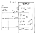
- a three-wire transmission line comprising a tip conductor with terminal nodes 101 and 102, a ring conductor with terminal nodes 103 and 104 and a circuit ground with nodes 105 and 106, is shown in FIG. 1 connecting a test position 200 and a remotely-located termination position 100.
- the DC resistance of the tip conductor and ring conductor between positions 100 and 200 is designated by resistors 121 and 122, respectively. In most situations, resistors 121 and 122 have substantially the same value.
- the illustrative circuit under test having a termination position 100 can be synthesized by a three terminal equivalent circuit 110.
- Circuit 110 comprises tip-ring resistor 123, ring-ground resistor 124 in series with a DC source 125, and tip-ground resistor 126 in series with another DC source 127.
- Each DC source in FIG. 1 is represented by a battery.
- This DC three terminal equivalent circuit is representative of a class of telecommunications circuits which are tested.
- the three terminal equivalent circuit represents other passive networks, such as a coin telephone, which can be conducted to a three terminal transmission line.
- an AC three terminal equivalent circuit results, which also can be analyzed to determine circuit faults in a class of telecommunications circuits which are tested.
- the circuit element values for the three terminal equivalent circuit can be determined using measurements taken at test position 200 in a well-known fashion.
- the tip and ring resistors 121 and 122 are combined with the other resistors, 123, 124 and 126 to arrive at the three terminal equivalent circuit of FIGS. 2 ad 3.
- This combination provides no limitation as the values of resistors 121 and 122 can be readily subtracted from the determined circuit element values to obtain the corresponding circuit element values of three terminal equivalent circuit 110.
- the determined value of R12 is substantially different from its true value. This significant error arises whenever one circuit element value in the three terminal equivalent circuit is significantly different from the others.
- FIG. 3 shows the improved accuracy in the determined circuit element values resulting from the use of the present invention which utilizes at least one ratio, the numerator and denominator of each ratio being a different function of at least one of the measurements determined at test position 200.
- This ratio is then used to determine the values of the circuit elements.
- Each ratio of the measurement functions is representative of the ratio of the true values of one selected circuit element to another in the three terminal equivalent circuit.
- the accuracy of the measurement function ratio to the ratio of the true values of the selected circuit elements varies with the internal resistance of the measuring equipment. Ideally, i.e., in the absence of such internal resistance and measurement error, each ratio of the measurement functions is equal to the ratio of selected circuit element values.
- a predetermined voltage source and a serially connected predetermined, source protection resistor is sequentially connected between first and second preselected pairs of terminals.
- the two preselected pairs of terminals are tip-to-ground and ring-to-ground, it, of course, being understood that any two pairs of terminals could be selected.
- the value of the source protection resistor should be large enough to limit the current flowing through the source to a safe level. The voltages measured are used to determine the appropriate values of the source protection resistor for signal source connection between each pair of terminals.
- the determined value of the source protection resistor for each pair of terminals is used when performing succeeding measurements since a more accurate determination of the resistor values in the three-terminal equivalent network can be made when the resistance of the source protection resistor is closely matched to the equivalent resistance between the selected terminal pairs and yet be large enough to prevent a damage to the measurement equipment. Similarly, the value of the voltage source should be large enough to get accurate measurements while not causing a current flow in the circuit under test which exceeds the maximum levels.
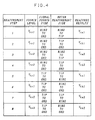
- the appropriately valued source protection resistor corresponding to each of the preselected pairs of terminals is used in all of the measurement steps shown in FIG. 4.
- step 1 signal source apparatus comprising a voltage source having a first predetermined level, V rs 1 , and a serially connected protection resistor, R p 1 , is applied across the ring and ground terminals and a voltage measurement between the ring and tip terminals is made, designated as V ra 1 .
- step 2 the signal source apparatus of step 1 is left unchanged and a voltage measurement between the tip and ground terminals, designated as V rb 1 , is made.
- steps 3 and 4 the signal source apparatus is left unchanged but set to another source level, V rs 2 , and voltage measurements across ring to tip, V ra 2 , and tip to ground, V rb 2 , are made.
- Source levels V rs 1 and V rs 2 are selected so as to provide the maximum possible voltage swing between these levels.
- the total resistance of the three terminal equivalent circuit viewed between the ring to ground terminals, R x 1 can be determined in accordance with the following relationship: and a ratio K 2 can be formed in accordance with the following expression:
- the ratio K2 is representative or is an estimate of the ratio of the values of resistors R2/R12.
- the signal source apparatus and serially connected source protection resistor, R p 2 are connected between the tip and ground terminals.
- steps 5 and 6 a source level designated as V ts 1 is applied.
- the measurement meter is respectively connected between the tip and ring and ring and ground terminals to provide measurements V ta 1 and V tb 1 .
- steps 7 and 8 using an associated source level V ts 2 to determine the measurements V ta 2 and V tb 2 .
- Source levels V ts 1 and V ts 2 are selected with the same guidelines used for V rs 1 and V rs 2 .
- the total resistance, R x 2 , of the three terminal equivalent network viewed between the tip and ground terminals and the ratio K1 can be determined, where Again, with the signal source apparatus connected between tip and ground, the current through resistors R1 and R12 is the same and K 1 is an estimate of the ratio of resistors R1/R12. Furthermore, K 1 is equal to this resistor value ratio in the absence of measurement errors and the effect of the meter's internal resistance.
- Resistor R 12 in the illustrative three terminal equivalent circuit can be determined in accordance with equation 7 or 8.
- the equation used should be the one wherein the ratio K 1 or K 2 in the second term of the equation, i.e., has the smallest error.
- the error for the ratio K 1 or K 2 can be determined, in well-known fashion, from the known or estimated error associated with each measurement used to form the ratio. This ratio error determination is even simpler for certain three terminal equivalent circuits where the ratio with the smallest error is the ratio closest to one. Such is the case for a three terminal equivalent circuit including only resistors between the tip, ring and ground terminals.
- the values of E 1 and E 2 can be readily determined from a number of different mathematical expressions.
- the presence of the meter's internal resistance during a measurement alters the element values of the three terminal equivalent circuit viewed from the test position. Furthermore, this alteration varies as the meter connections change from one pair of terminals to another.
- one or more compensating resistors each having a value equal to that of the meter's internal resistance, is advantageously connected between one or more pairs of terminals so as to maintain the same equivalent circuit element values as the meter connections are changed.
- R m The effect of the compensating resistor, designated as R m , can then be readily subtracted from the determinations of R 1, R 2 and R 12.
- R n R 1, R 2 or R 12
- R ' n the corresponding resistor value corrected for the addition of compensating resistor R m
- E' n is the corresponding battery value corrected for the presence of R m .
- the present invention can be adapted to compensate for different sources of measurement error.
- the value of resistor R12 is very much greater than the values of the resistors R 1 and R2 and the values of E 1 and E 2 exceed a predetermined threshold value.
- a measurement error has occurred due to the bib effect of a battery element in the three terminal equivalent circuit.
- This error can be reduced by employing a bias compensation technique which utilizes additional measurements to improve the accuracy of the determined value of resistor R 12. Pursuant to this technique, the ratio K 1 and K 2 having the largest value is selected, and certain measurements used in calculating the selected ratio are repeated using a biasing voltage.
- the repeated measurements are those which were made between a pair of terminals whose directly interconnecting equivalent circuit path includes a battery element. Specifically, if ratio K 1 is selected, measurement steps 6 and 8 are repeated with a biasing voltage in series with the measurement meter. The value of the biasing voltage is equal to the determined value of element E 1 or the average value of V tb 1 and V tb 2 . If ratio K 2 is selected, measurement steps 2 and 4 are repeated with a biasing voltage equal to the determined value of element E 2 or the average of V rb 1 and V rb 2 serially connected to the measurement meter. Using these two additional measurements, the value of the selected ratio is recalculated and then the value of element R 12 is calculated using the equation in which the selected ratio appears in the denominator of the second term.
- ratios K 1 or K 2 are arbitrarily selected and the measurement steps used to form the selected ratio are repeated. These measurements are preferably repeated with a source protection resistor having a revised value to reflect the addition of the external resistor. Specifically, for ratio K 1, measurement steps 5 through 8 are repeated with an external resistor coupled between the ring and ground terminals. Similarly, for ratio K 2, measurement steps 1 through 4 are repeated with an external resistor coupled between the tip and ground terminals. In either case, the value of the external resistor should be small enough to reduce the value of the selected ratio below a preselected maximum value.
- bias compensation and ratio reduction technique can be incorporated together into the present invention or, in certain applications, either one alone may be so incorporated.
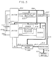
- FIG. 5 shows a block-schematic diagram of apparatus which performs the measurement methodology described hereinabove for a three terminal equivalent circuit.
- controller 507 directs switch 501, via bus 508, to connect measurement meter 509 across the ring to ground and tip to ground terminals to provide a pair of voltage measurements.
- a predetermined DC voltage is provided by source 506 across leads 503 and 516 and a predetermined resistor from source protection resistor selector 505 is inserted between leads 502 and 516.
- Switch 501 controlled by controller 507 via bus 508, respectively connects leads 502 and 503 to the ring and ground terminals and then to the tip and ground terminals.
- switch 501 sequentially connects leads 510 and 511 of measurement meter 509 to these terminal pairs to provide a pair of voltage measurements.
- switch 504 advantageously connects one or more compensating resistors from compensating resistor selector 515. Each resistor having a value equal to the internal resistance of the measurement meter, is connected between selected pairs of terminals so as to maintain the same equivalent circuit element values as the meter connections are changed.
- the four voltage measurements provided by meter 509 are coupled via bus 512 to processor 513 which determines the total resistance of the three terminal equivalent circuit between the ring and ground terminals and between the tip and ground terminals.
- Processor 513 selects a resistor having the closest value to each determined total resistance from a plurality of preselected resistors in selector 505.
- the selections made and the appropriate levels for source 506 are communicated to controller 507 via bus 514.
- Controller 507 directs selector 505 to insert a selected resistor between leads 502 and 516 when the source is coupled between a corresponding pair of circuit terminals.
- controller 507 via bus 508 sequentially directs switch 501 to provide the source and measurement meter connections as set forth in measurement steps 1-8 of FIG. 4. Controller 507 also controls the voltage level of source 506 and the operation of meter 509 for these steps via bus 508. In addition, controller 507 advantageously controls the operation of switch 504 so as to provide compensating resistors across the terminals during the measurement steps which maintain the same equivalent circuit element values as the meter connections are changed.
- Processor 513 determines the values of R x 1 , R x 2 , K 1 and K 2 and thence the circuit element values. The determined values are then examined by processor 513, and if they don't fall within predetermined categories, the determined values are coupled via bus 518 to output device 517. If however, the determined values fall within these categories, then either the bias compensation or the ratio reduction technique is instituted to further improve the accuracy of the determined value of R 12.
- the appropriate technique to use along with the source levels, necessary biasing voltage external resistor value, source protection resistor value, and source and meter connections are communicated to controller 507 via bus 514.
- the required biasing voltage is provided within meter 509 under the control of controller 507.
- compensating resistor selector 515 provides the approximately-valued external resistor for the ratio reduction technique via signals on bus 508 from controller 507.
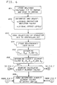
- FIGS. 6 and 7 set forth the operations of processor 513.
- operations 601-603 the four tip to ground and ring to ground voltages are stored and the values of the source protection resistors for ring to ground and tip to ground source connections are calculated.
- the measurements made during steps 1-8 are supplied by bus 512 to processor 513 and stored therein as shown by operation 604. These stored measurements are then selectively used, as shown by operation 605, to calculate the equivalent resistances R x 1 and R x 2 and the ratios K 1 and K 2 as previously described.
- These four quantities, as depicted by operation 606, are used to determine the values of all the circuit elements.
- Operation 607 designates the examination of the relative values of the circuit element values to determine whether the bias compensation or ratio reduction technique should be applied. If not, the determined results are coupled, as illustrated by operation 608 to the output device. If the bias compensation technique should be applied, operations 701-705 illustrate the sequentially steps provided by processor 513. Similarly, operations 706-710 illustrate the sequential procedures performed by processor 513 when the ratio reduction technique is used.
- the present invention can also be applied after conventional techniques have been used to determine the described circuit element values and one or more of said values is inaccurate.
- only one resistor value is incorrect and the present invention can be used to correct this value.
- only one ratio need be formed from the associated measurements. The inaccurate circuit clement value is then corrected using this ratio.
- the circuit elements are impedances having a real and imaginary part.
- the signal applied to the three terminal equivalent circuit is from an AC source and the measurements taken involve the use of a demodulator and equipment which determines the magnitude and phase of the AC signal between the described circuit terminals.
- the computations in an AC characterization are the same as those disclosed except that for an AC characterization complex numbers are involved instead of the real numbers manipulated in a DC characterization.
Landscapes
- Engineering & Computer Science (AREA)
- Signal Processing (AREA)
- Physics & Mathematics (AREA)
- General Physics & Mathematics (AREA)
- Measurement Of Resistance Or Impedance (AREA)
Claims (20)
- Appareil de détermination de valeurs électriques d'éléments d'un circuit dans un circuit équivalent à trois bornes (R₁, R₂, R₁₂, E₁, E₂), ledit circuit équivalent étant représentatif d'un réseau réel de communications, ledit appareil incluant des moyen (501, 504 à 507, 509, 513) d'application des signaux prédéterminés, audit réseau de communications, et de mesure des effets électriques en réponse à ceux-ci, et CARACTERISE PAR des moyens (513, 605) de formation d'au moins un rapport (par exemplele numérateur et le dénominateur du rapport ou de chacun d'eux étant exclusivement une fonction desdits effets mesurés et le rapport ou chacun d'eux étant représentatif du rapport entre les valeurs d'impédance d'un élément de circuit choisi au préalable (R₁) et d'un autre élément de circuit choisi au préalable (R₁₂) dans ledit circuit équivalent et des moyens (513, 506) de détermination des valeurs électriques desdits éléments d'un circuit, en réponse à au moins l'un desdits rapports.

- Appareil selon la revendication 1 dans lequel ledit moyen d'application sert à coupler audit réseau un élément protecteur (505).
- Appareil selon la revendication 1 ou 2 dans lequel ledit moyen d'application inclut un instrument de mesure (509) à résistance interne.
- Appareil selon la revendication 3 dans lequel ledit moyen d'application inclut un moyen (515) de couplage d'un élément auxiliaire de circuit audit réseau de manière à compenser ladite résistance interne, tandis que les valeurs des éléments d'un circuit équivalent, sont maintenues dans ledit circuit équivalent.
- Appareil selon une revendication précédente quelconque dans lequel ledit moyen de détermination sert à examiner lesdites valeurs des éléments d'un circuit et à déterminer quand ces valeurs sont situées à l'intérieur d'au moins une plage prédéterminée.
- Appareil selon la revendication 5 dans lequel ledit moyen de détermination sert à ordonner auxdits moyens d'application d'appliquer des signaux supplémentaires audit réseau et à mesurer les effets électriques en réponse à ceux-ci lorsque lesdites valeurs sont situées à l'intérieur de ladite plage.
- Appareil selon la revendication 6 dans lequel ledit moyen d'application sert à appliquer audit réseau un élément de circuit externe lors de la mesure des effets électriques desdits signaux supplémentaires.
- Appareil selon la revendication 6 dans lequel ledit moyen d'application sert à appliquer audit réseau un signal de polarisation lors de la mesure des effets électriques desdits signaux supplémentaires.
- Appareil selon la revendication 6, 7 ou 8, dans lequel ledit moyen de détermination sert à réviser certaines desdites valeurs d'éléments d'un circuit, en réponse aux effets électriques mesurés desdits signaux supplémentaires.
- Appareil selon une revendication précédente quelconque dans lequel le rapport formé par ledit moyen de formation, ou chacun de ces rapports, est proportionnel au rapport entre la valeur électrique d'un élément de circuit choisi au préalable et un autre élément dudit circuit équivalent.
- Procédé de détermination des valeurs électriques d'éléments d'un circuit dans un circuit équivalent à trois bornes (R₁, R₂, R₁₂, E₁, E₂) ledit circuit équivalent étant représentatif d'un réseau réel de communications, ledit procédé comprenant les étapes consistant à appliquer (501, 504 à 507, 509, 513, 613) des signaux prédéterminés, audit réseau de communications, et à mesurer les effets électriques en réponse à ceux-ci, et CARACTERISE PAR une formation (513, 605) d'au moins un rapport (par exempleen utilisant un appareil à processeur (513), le numérateur et le dénominateur du rapport ou de chacun d'eux étant exclusivement une fonction desdits effets mesurés et le rapport ou chacun d'eux étant représentatif du rapport entre les valeurs d'impédance d'un élément de circuit choisi au préalable (R₁) et d'un autre élément de circuit choisi au préalable (R₁₂) dans ledit circuit équivalent, et à déterminer (513, 606) les valeurs électriques desdits éléments d'un circuit, en réponse à au moins l'un desdits rapports en utilisant ledit appareil à processeur.
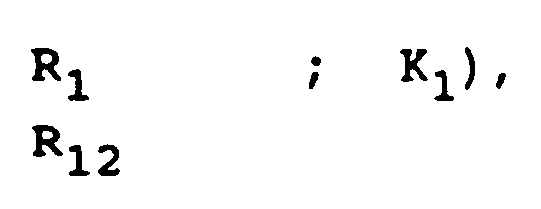
- Procédé selon la revendication 11 incluant l'étape consistant à coupler un élément protecteur (505) de circuit audit réseau lors de l'application desdits signaux prédéterminés.
- Procédé selon la revendication 11 ou 12 dans lequel la mesure des effets électriques desdits signaux appliqués sur ledit réseau est effectuée à l'aide d'un instrument (509) à résistance interne.
- Procédé selon la revendication 13 incluant l'étape consistant à coupler audit réseau un élément auxiliaire (515) de circuit afin de compenser ladite résistance interne lors de l'application des signaux prédéterminés, tandis que des valeurs d'éléments d'un circuit équivalent sont maintenues dans ledit circuit équivalent.
- Procédé selon l'une quelconque des revendications 11 à 14 incluant l'étape consistant à déterminer quand les valeurs des éléments d'un circuit sont situées à l'intérieur d'au moins une plage prédéterminée.
- Procédé selon la revendication 15 incluant l'étape consistant à appliquer des signaux supplémentaires audit réseau et à mesurer la réponse à ceux-ci lorsque lesdites valeurs sont situées à l'intérieur de ladite plage.
- Procédé selon la revendication 16 incluant l'étape consistant à coupler audit réseau un élément extérieur de circuit lors de la mesure des effets électriques desdits signaux supplémentaires.
- Procédé selon la revendication 16 incluant l'étape consistant à appliquer audit réseau un signal de polarisation lors de la mesure des effets électriques desdits signaux supplémentaires.
- Procédé selon la revendication 16, 17 ou 18 incluant l'étape consistant à réviser certaines desdites valeurs d'éléments d'un circuit en réponse à la mesure des effets électriques desdits signaux supplémentaires.
- Procédé selon l'une quelconque des revendications 11 à 19 dans lequel le rapport ou chacun d'eux est proportionnel au rapport entre la valeur électrique d'un élément de circuit choisi au préalable et celle d'un autre élément dudit circuit équivalent.
Applications Claiming Priority (2)
| Application Number | Priority Date | Filing Date | Title |
|---|---|---|---|
| US07/033,445 US4797622A (en) | 1987-04-01 | 1987-04-01 | Technique for determining the values of circuit elements in a three terminal equivalent circuit |
| US33445 | 1987-04-01 |
Publications (2)
| Publication Number | Publication Date |
|---|---|
| EP0285320A1 EP0285320A1 (fr) | 1988-10-05 |
| EP0285320B1 true EP0285320B1 (fr) | 1993-11-24 |
Family
ID=21870440
Family Applications (1)
| Application Number | Title | Priority Date | Filing Date |
|---|---|---|---|
| EP88302587A Expired - Lifetime EP0285320B1 (fr) | 1987-04-01 | 1988-03-24 | Dispositif et méthode pour la détermination des valeurs des éléments d'un circuit équivalent à trois pôles |
Country Status (6)
| Country | Link |
|---|---|
| US (1) | US4797622A (fr) |
| EP (1) | EP0285320B1 (fr) |
| JP (1) | JPH0718901B2 (fr) |
| KR (1) | KR930003854B1 (fr) |
| CA (1) | CA1286363C (fr) |
| DE (1) | DE3885782T2 (fr) |
Families Citing this family (3)
| Publication number | Priority date | Publication date | Assignee | Title |
|---|---|---|---|---|
| US5054050A (en) * | 1990-04-30 | 1991-10-01 | American Telephone & Telegraph Co. | Drop testing in fiber to the home systems |
| EP0961467A1 (fr) * | 1998-05-27 | 1999-12-01 | Porta Systems Corporation | Appareil et méthode pour tester un système de télécommunication |
| DE102006025672B4 (de) * | 2006-06-01 | 2008-02-28 | Infineon Technologies Ag | Niedervolt-Baustein in einem analogen Telefondienstsystem und Verfahren zur Korrektur einer durch einen Leckstrom verursachten temperaturabhängigen Offsetspannung |
Family Cites Families (12)
| Publication number | Priority date | Publication date | Assignee | Title |
|---|---|---|---|---|
| US3646435A (en) * | 1970-06-08 | 1972-02-29 | Eliokim Zelikovich Rozenson | Wheatstone-thomson combined electrical measuring bridge |
| US4028507A (en) * | 1976-06-28 | 1977-06-07 | Bell Telephone Laboratories, Incorporated | Apparatus for applying particular voltages to three-terminal circuits and measuring resulting current flows for the purpose of determining circuit characteristics |
| FR2358074A1 (fr) * | 1976-07-09 | 1978-02-03 | Ericsson Telefon Ab L M | Dispositif automatique d'essai des lignes et postes d'abonnes d'une installation telephonique |
| USRE30692E (en) * | 1980-03-24 | 1981-07-28 | Northern Telecom Limited | Method and apparatus for measuring telephone line characteristics |
| GB2093292A (en) * | 1981-02-18 | 1982-08-25 | Riggs William | Apparatus and methods for analogue-to-digital conversion and for deriving in-phase and quadrature components of voltage and current in an impedance |
| US4424479A (en) * | 1981-10-05 | 1984-01-03 | Bell Telephone Laboratories, Incorporated | Loop fault location |
| US4410850A (en) * | 1981-10-16 | 1983-10-18 | Bell Telephone Laboratories, Incorporated | Water-compensated open fault locator |
| US4538105A (en) * | 1981-12-07 | 1985-08-27 | The Perkin-Elmer Corporation | Overlay test wafer |
| US4578761A (en) * | 1983-03-25 | 1986-03-25 | At&T Bell Laboratories | Separating an equivalent circuit into components to detect terminating networks |
| US4501935A (en) * | 1983-07-20 | 1985-02-26 | At&T Bell Laboratories | Detecting a DC nonlinearity terminating a network |
| US4714874A (en) * | 1985-11-12 | 1987-12-22 | Miles Inc. | Test strip identification and instrument calibration |
| JPS62118264A (ja) * | 1985-11-19 | 1987-05-29 | Sakata Denki Kk | ケ−ブル抵抗補正機能を備えた可変抵抗器の抵抗比測定方式 |
-
1987
- 1987-04-01 US US07/033,445 patent/US4797622A/en not_active Expired - Lifetime
-
1988
- 1988-03-24 EP EP88302587A patent/EP0285320B1/fr not_active Expired - Lifetime
- 1988-03-24 DE DE3885782T patent/DE3885782T2/de not_active Expired - Fee Related
- 1988-03-29 CA CA000562763A patent/CA1286363C/fr not_active Expired - Lifetime
- 1988-03-31 JP JP63076673A patent/JPH0718901B2/ja not_active Expired - Fee Related
- 1988-03-31 KR KR8803579A patent/KR930003854B1/ko not_active Expired - Fee Related
Also Published As
| Publication number | Publication date |
|---|---|
| US4797622A (en) | 1989-01-10 |
| CA1286363C (fr) | 1991-07-16 |
| DE3885782T2 (de) | 1994-06-01 |
| KR930003854B1 (en) | 1993-05-14 |
| JPS63261177A (ja) | 1988-10-27 |
| DE3885782D1 (de) | 1994-01-05 |
| EP0285320A1 (fr) | 1988-10-05 |
| JPH0718901B2 (ja) | 1995-03-06 |
| KR880013355A (ko) | 1988-11-30 |
Similar Documents
| Publication | Publication Date | Title |
|---|---|---|
| US6084946A (en) | Qualifying a telephone line for digital transmission service | |
| US5864602A (en) | Qualifying telephone line for digital transmission service | |
| US6756786B2 (en) | Method for detecting line-to-ground fault location in power network | |
| US4103225A (en) | System and method for determining capacitance and cable length in the presence of other circuit elements | |
| EP0327191B1 (fr) | Dispositif de localisation de défaults ohmique et dispositif pour l'utilisation a câbles | |
| US3248646A (en) | Location of cable faults by comparing a section of the faulted cable with a part of the section | |
| US6680616B2 (en) | In-service testing of current transformers | |
| US5436953A (en) | Digital longitudinal balance measurement | |
| US4400663A (en) | Shunt fault tester for multiconductor cable | |
| JP7039149B2 (ja) | 故障点距離検出装置 | |
| US4424479A (en) | Loop fault location | |
| US3234459A (en) | Method and apparatus for locating faults in electrical cable lines by comparing the impedance of the entire faulted line to the impedance of a section of the line | |
| EP0003433A1 (fr) | Perfectionnements à la localisation de défauts de contacts dans des câbles électriquement conducteurs | |
| US4399402A (en) | Resistive fault sectionalization | |
| EP4257987B1 (fr) | Procédé de localisation d'un point de défaut sur un câble haute tension ca triphasé et système de localisation d'un point de défaut | |
| US5307019A (en) | Method and apparatus for determining the weld and coil resistances of a motor winding | |
| US4797622A (en) | Technique for determining the values of circuit elements in a three terminal equivalent circuit | |
| EP0206161A2 (fr) | Dispositif automatique de localisation de défauts dans des lignes téléphoniques | |
| US6590962B1 (en) | Method of performing non-interactive resistive fault location | |
| US4410850A (en) | Water-compensated open fault locator | |
| US5216373A (en) | Circuit element measuring apparatus and method for measuring a parameter of a DUT including a compensation network having an admittance characteristic | |
| WO1990011533A2 (fr) | Detection de defauts dans des cables | |
| CA2179249C (fr) | Reperage de defauts resistifs | |
| JP3147987B2 (ja) | 平衡系特性パラメータ測定装置および測定方法 | |
| US7801697B2 (en) | Method and device for testing communication circuits |
Legal Events
| Date | Code | Title | Description |
|---|---|---|---|
| PUAI | Public reference made under article 153(3) epc to a published international application that has entered the european phase |
Free format text: ORIGINAL CODE: 0009012 |
|
| AK | Designated contracting states |
Kind code of ref document: A1 Designated state(s): DE FR GB NL |
|
| 17P | Request for examination filed |
Effective date: 19890328 |
|
| 17Q | First examination report despatched |
Effective date: 19910619 |
|
| GRAA | (expected) grant |
Free format text: ORIGINAL CODE: 0009210 |
|
| AK | Designated contracting states |
Kind code of ref document: B1 Designated state(s): DE FR GB NL |
|
| REF | Corresponds to: |
Ref document number: 3885782 Country of ref document: DE Date of ref document: 19940105 |
|
| ET | Fr: translation filed | ||
| RAP4 | Party data changed (patent owner data changed or rights of a patent transferred) |
Owner name: AT&T CORP. |
|
| PLBE | No opposition filed within time limit |
Free format text: ORIGINAL CODE: 0009261 |
|
| STAA | Information on the status of an ep patent application or granted ep patent |
Free format text: STATUS: NO OPPOSITION FILED WITHIN TIME LIMIT |
|
| 26N | No opposition filed | ||
| PGFP | Annual fee paid to national office [announced via postgrant information from national office to epo] |
Ref country code: FR Payment date: 20000223 Year of fee payment: 13 |
|
| PGFP | Annual fee paid to national office [announced via postgrant information from national office to epo] |
Ref country code: GB Payment date: 20000225 Year of fee payment: 13 |
|
| PGFP | Annual fee paid to national office [announced via postgrant information from national office to epo] |
Ref country code: NL Payment date: 20000316 Year of fee payment: 13 |
|
| PGFP | Annual fee paid to national office [announced via postgrant information from national office to epo] |
Ref country code: DE Payment date: 20000331 Year of fee payment: 13 |
|
| PG25 | Lapsed in a contracting state [announced via postgrant information from national office to epo] |
Ref country code: GB Free format text: LAPSE BECAUSE OF NON-PAYMENT OF DUE FEES Effective date: 20010324 |
|
| PG25 | Lapsed in a contracting state [announced via postgrant information from national office to epo] |
Ref country code: NL Free format text: LAPSE BECAUSE OF NON-PAYMENT OF DUE FEES Effective date: 20011001 |
|
| GBPC | Gb: european patent ceased through non-payment of renewal fee |
Effective date: 20010324 |
|
| PG25 | Lapsed in a contracting state [announced via postgrant information from national office to epo] |
Ref country code: FR Free format text: LAPSE BECAUSE OF NON-PAYMENT OF DUE FEES Effective date: 20011130 |
|
| NLV4 | Nl: lapsed or anulled due to non-payment of the annual fee |
Effective date: 20011001 |
|
| REG | Reference to a national code |
Ref country code: FR Ref legal event code: ST |
|
| PG25 | Lapsed in a contracting state [announced via postgrant information from national office to epo] |
Ref country code: DE Free format text: LAPSE BECAUSE OF NON-PAYMENT OF DUE FEES Effective date: 20020101 |