EP0285344A2 - Verfahren zum Verzweigen und Anschliessen von Flachkabeln - Google Patents
Verfahren zum Verzweigen und Anschliessen von Flachkabeln Download PDFInfo
- Publication number
- EP0285344A2 EP0285344A2 EP88302694A EP88302694A EP0285344A2 EP 0285344 A2 EP0285344 A2 EP 0285344A2 EP 88302694 A EP88302694 A EP 88302694A EP 88302694 A EP88302694 A EP 88302694A EP 0285344 A2 EP0285344 A2 EP 0285344A2
- Authority
- EP
- European Patent Office
- Prior art keywords
- portions
- leads
- flat cable
- earth
- signal
- Prior art date
- Legal status (The legal status is an assumption and is not a legal conclusion. Google has not performed a legal analysis and makes no representation as to the accuracy of the status listed.)
- Withdrawn
Links
Images




Classifications
-
- H—ELECTRICITY
- H01—ELECTRIC ELEMENTS
- H01R—ELECTRICALLY-CONDUCTIVE CONNECTIONS; STRUCTURAL ASSOCIATIONS OF A PLURALITY OF MUTUALLY-INSULATED ELECTRICAL CONNECTING ELEMENTS; COUPLING DEVICES; CURRENT COLLECTORS
- H01R43/00—Apparatus or processes specially adapted for manufacturing, assembling, maintaining, or repairing of line connectors or current collectors or for joining electric conductors
-
- H—ELECTRICITY
- H01—ELECTRIC ELEMENTS
- H01R—ELECTRICALLY-CONDUCTIVE CONNECTIONS; STRUCTURAL ASSOCIATIONS OF A PLURALITY OF MUTUALLY-INSULATED ELECTRICAL CONNECTING ELEMENTS; COUPLING DEVICES; CURRENT COLLECTORS
- H01R12/00—Structural associations of a plurality of mutually-insulated electrical connecting elements, specially adapted for printed circuits, e.g. printed circuit boards [PCB], flat or ribbon cables, or like generally planar structures, e.g. terminal strips, terminal blocks; Coupling devices specially adapted for printed circuits, flat or ribbon cables, or like generally planar structures; Terminals specially adapted for contact with, or insertion into, printed circuits, flat or ribbon cables, or like generally planar structures
- H01R12/70—Coupling devices
- H01R12/77—Coupling devices for flexible printed circuits, flat or ribbon cables or like structures
- H01R12/771—Details
- H01R12/775—Ground or shield arrangements
-
- H—ELECTRICITY
- H01—ELECTRIC ELEMENTS
- H01R—ELECTRICALLY-CONDUCTIVE CONNECTIONS; STRUCTURAL ASSOCIATIONS OF A PLURALITY OF MUTUALLY-INSULATED ELECTRICAL CONNECTING ELEMENTS; COUPLING DEVICES; CURRENT COLLECTORS
- H01R12/00—Structural associations of a plurality of mutually-insulated electrical connecting elements, specially adapted for printed circuits, e.g. printed circuit boards [PCB], flat or ribbon cables, or like generally planar structures, e.g. terminal strips, terminal blocks; Coupling devices specially adapted for printed circuits, flat or ribbon cables, or like generally planar structures; Terminals specially adapted for contact with, or insertion into, printed circuits, flat or ribbon cables, or like generally planar structures
- H01R12/50—Fixed connections
- H01R12/59—Fixed connections for flexible printed circuits, flat or ribbon cables or like structures
-
- H—ELECTRICITY
- H01—ELECTRIC ELEMENTS
- H01R—ELECTRICALLY-CONDUCTIVE CONNECTIONS; STRUCTURAL ASSOCIATIONS OF A PLURALITY OF MUTUALLY-INSULATED ELECTRICAL CONNECTING ELEMENTS; COUPLING DEVICES; CURRENT COLLECTORS
- H01R13/00—Details of coupling devices of the kinds covered by groups H01R12/70 or H01R24/00 - H01R33/00
- H01R13/648—Protective earth or shield arrangements on coupling devices, e.g. anti-static shielding
- H01R13/658—High frequency shielding arrangements, e.g. against EMI [Electro-Magnetic Interference] or EMP [Electro-Magnetic Pulse]
- H01R13/6581—Shield structure
- H01R13/6585—Shielding material individually surrounding or interposed between mutually spaced contacts
- H01R13/6588—Shielding material individually surrounding or interposed between mutually spaced contacts with through openings for individual contacts
-
- H—ELECTRICITY
- H01—ELECTRIC ELEMENTS
- H01R—ELECTRICALLY-CONDUCTIVE CONNECTIONS; STRUCTURAL ASSOCIATIONS OF A PLURALITY OF MUTUALLY-INSULATED ELECTRICAL CONNECTING ELEMENTS; COUPLING DEVICES; CURRENT COLLECTORS
- H01R13/00—Details of coupling devices of the kinds covered by groups H01R12/70 or H01R24/00 - H01R33/00
- H01R13/648—Protective earth or shield arrangements on coupling devices, e.g. anti-static shielding
- H01R13/658—High frequency shielding arrangements, e.g. against EMI [Electro-Magnetic Interference] or EMP [Electro-Magnetic Pulse]
- H01R13/6591—Specific features or arrangements of connection of shield to conductive members
- H01R13/6592—Specific features or arrangements of connection of shield to conductive members the conductive member being a shielded cable
Definitions
- the present invention relates to a method of forming branch connection with a flat cable, and in particular to a method of forming electrical connections for connecting an intermediate portion of, for example, a high-speed signal transfer cable to contacts of a connector for branching connection.
- the cable was cut into two portions 101, 102 as shown in Figure 14, the leads 101a, 101b, 101c,..., 102a, 102b, 102c, ..., of respective cables 101, 102 being exposed at the cut ends 103, 104 of these cable portions 101, 102; pairs of corresponding leads 101a, 102a; 101c, 102c, ... ..., are electrically connected to the end portions of respective contacts 105, 106, 107, ... ..., by means of, for example, soldering.
- the present invention has been made in view of the above mentioned point, and an object thereof is to provide a method which makes it possible to form good branch connections of a flat cable easily and securely, and which further makes it possible to reduce the variation in the impedances, even for high-speed signals or signals having very high frequency components, at the branch connections of a transfer system.
- a method of forming branch connection of a flat cable comprising the steps of: removing an insulation coating of a flat cable in a transverse direction relative to the flat cable at three longitudinal portions thereof, thereby exposing all of the leads of the flat cable at said three portions; folding the flat cable at the intermediate exposed lead portion of said three portions; causing each of the earth leads of the leads of the flat cable at the exposed portions to project toward a nearer surface; causing the signal leads of the leads of the flat cable at the exposed lead portions to project toward the folded ends thereof keeping the folded condition thereof; electrically connecting the earth leads on both surfaces of overlapped portions to a common earth lead connecting means at said both surfaces; and electrically connecting each of the folded projecting portions of the signal leads and of the common earth lead connecting means to a corresponding connection terminal of branch signal output means.
- each of the earth leads among the leads of a flat cable is caused to project to and from the nearer surface side of overlapped portions, the earth leads on both surfaces of the overlapped portions are electrically connected on said both surfaces to a common earth lead connecting means, and signal leads among the leads of the flat cable at the folded exposed lead portions are caused to project to and from their folded end side in the folded condition without being cut, whereby the earth leads and signal leads can be securely spaced apart and only the signal leads are caused to project to the folded end side, so that there is little fear of short circuiting or imperfect connections between the signal leads and thus good branch connections can be formed.
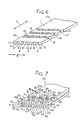
- FIGs 1 through 13, 1 represents a flat cable for signal transfer between high-speed signal processing units such as computers and their peripheral processing units, an insulating or dielectric coating 2 of the flat cable 1 having embedded therein a large number (generally up to 50 - 60, but, for simplicity the following description will be given in conjunction with the drawings as to the case of four) of signal transfer leads 3, 4, 5, 6 and twice as many earth leads 7, 8, 9, 10, 11, 12, 13, 14 as the signal transfer lead is located between a pair of earth leads in order that cross-talk of the signals between the signal lines may be suppressed.
- a large number generally up to 50 - 60, but, for simplicity the following description will be given in conjunction with the drawings as to the case of four
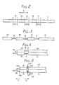
- the insulating coating 2 is removed in the transverse direction B, see Figure 6, at three portions 15, 16, 17 which are equally spaced apart in the longitudinal direction A of the flat cable 1.
- the insulating coating 2 may also be removed at more than three portions, for example, at five or seven portions.
- a laser such as a CO2 laser may be used; alternatively, any mechanical, chemical or thermal means may be used.
- the removal of the insulation coating removes all insulation coating at the portions 15, 16 and 17, exposing all the signal leads 3 through 6 and earth leads 7 through 14 thereat.
- the flat cable 1 is folded at the intermediate lead exposed portion 16 in a manner such that the insulation coating residual portions 18, 19 and insulation coating portions 20, 21 on both sides, as well as the exposed lead portions 15, 17, are overlapped on one another (exposed portions 15, 17 may be positioned in a not overlapped but shifted manner).
- the earth leads 7 through 14 are cut at their portions which correspond to the exposed portion 16. Such cutting of the earth leads 7 through 14 may be done before or after the folding, and in some cases it may be done simultaneously with the said removal of the insulation coating.
- the folded ends 3a, 4a, 5a, 6a of the respective signal lead 3, 4, 5, 6 are forced, without being cut, to project in the direction F, see Figure 5, out of the insulation coating portions 18, 19 to form electrical connections 3b, 4b, 5b, 6b, of the signal leads; earth lead portions 7a, 8a, 9a, 10a, 11a, 12a, 13a, and 14a at the exposed portion 15, which are located on the upper side in Figure 1 or in Figures 4 and 5 are pulled to project upwardly to form projections 7b, through 14b for electrical connection; earth lead portions 7c through 14c at the exposed portion 17, which are located on the lower side in Figures 4 and 5, are pulled to project downwardly to form projections 7d through 14d for electrical connection (lead portions 7c through 14c and 7d through 14d are similar to 7a through 14a and 7b through 14b and thus are not shown).
- the insulation coating portions 18, 19 are displaced toward the insulation coating portions 20, 21 in a direction G, see Figure 5, and the folded portions 3a, 4a, 5a, 6a of the corresponding leads 3, 4, 5, 6 are drawn out of the insulation coating portions 18, 19 in the direction F without being cut.
- the lead portions 7a through 14a are pulled in the direction G relative to the insulation coating portion 18 until their cut ends 7e through 14e reach the end face 18a of the insulation coating portion 18, while lead portions 7c through 14c are pulled in the direction G relative to the insulation coating portion 19 until their cut ends 7f through 14f reach the end face 19a of the insulation coating portion 19.
- the cut ends 7e through 14e, 7f through 14f are preferably retracted from the end faces 18a, 19a.
- an electrically conductive cover 22 for a common earth ground as the common earth lead connecting means is covered with an electrically conductive cover 22 for a common earth ground as the common earth lead connecting means.
- This cover 22 is formed by punching or blanking a thin metal plate of, for example, a copper alloy, and comprises a flat plate portion 23 located on the insulation coating portions 18, 20, a flat plate portion 24 located on the outer surfaces of the insulation coating portions 19, 21, and folded connecting portions 25, 26, 27.
- the cover 22 may also be constituted by a sheet-like member of a material such as plastics which is highly electrically insulating even for high frequency signals and which has a thin metal layer of, for example, copper formed on one surface (outer surface) thereof.
- the flat plate portion 23 has openings 28, 29, 30, 31, 32 formed therein, into which earth projections 7b, 8b, 9b, 10b, 11b, 12b, 13b, and 14b are inserted, while the flat plate portion 24 has openings 33, 34, 35, 36, 37 formed therein, into which earth projections 7d, 8d, 9d, 10d, 11d, 12d, 13d, 14d are inserted. Further, instead of one opening 29 into which earth projections 8b, 9b, are inserted, small openings for individual insertion of them may be provided in the flat plate portion 23.
- the corresponding earth projections 7b through 14b, 7d through 14d inserted into respective openings 28 through 39 are fixedly electrically connected to the openings 28 through 39 by soldering, for example.
- both side edge portions 23a, 24a and 23b, 24b are rigidly fixed together by means of, for example, welding, in order to place the overlapped insulation coating portions 18, 19 and 20, 21 in close contact with each other in the overlapping direction, to prevent the relative displacement of the insulation coating portions 18, 20 and 19, 21 in the direction along the overlapped surfaces, and to prevent the relative displacement among the signal lines such as lines 3, 4, 5 and 6 in the gap 49.
- the gap 49 may be filled with an electrically insulating resin, for example, to fix the signal lines such as lines 3, 4, 5, and 6 therein before or at a time of the mounting of this common earth cover 22.
- At least one of the coupling portions 25, 26, 27, for example the coupling portions 25, 27 on both sides, are engaged with connecting ends 41a, 42a of the contacts 41, 42 of a branch connection forming connector 50 as a branch signal output means having recesses 41b, 42b complementarily shaped to closely engage with the projecting ends 25a, 27a of the coupling portions 25, 27, and are easily and securely electrically connected and fixed by suitable means such as soldering. Further, as shown by imaginary lines in Figure 9, the intermediate coupling portion 26 may also be electrically connected to another similar connecting end.
- the projecting electrically connecting portions 3b, 4b, 5b, 6b of the signal leads extend substantially in a parallel manner such that desired gaps can be formed therebetween, and they are engaged with recesses 43b, 44b, 45b, 46b at connecting ends 43a, 44a, 45a, 46a of contacts 43, 44, 45, 46 of the branch connection forming connector 50, which recesses are similar to the recesses 41b, 42b of the connecting ends 41a, 42a of the contacts 41, 42 and are easily and securely electrically connected by means of soldering, for example.
- the connecting ends 43a through 46a electrically connected to the projecting electrically connecting portions 3b, 4b, 5b, and 6b of the signal leads may have suitable engaging structures such as holes instead of the recesses.
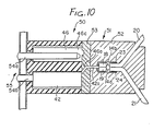
- An intermediate or branching connection portion 51 of the flat cable 1 constructed in the above mentioned manner is embedded in the resin 52, 53 using, for example, a suitable forming die such that it can be made integral with the connector 50.
- the contacts 41, 42, 43, 44, 45, and 46 of the connector 50 have female-type contact portions 41c, 42c, 43c, 44c, 45c, and 46c, see Figure 11, on the side opposite to the connecting ends 41a, 42a, 43a, 44a, 45a, and 46a.
- 54a, 54b, etc. represent the contacts of a male-type connector 55, see Figure 10, for engagement with the female-type contacts 41 through 46 of the connector 50.
- the connector 50 as the branching signal output means is described to be a female type connector in the explanations above, the branch signal output means may be a male-type connector or any other signal output mechanisms.
Landscapes
- Engineering & Computer Science (AREA)
- Manufacturing & Machinery (AREA)
- Multi-Conductor Connections (AREA)
- Coupling Device And Connection With Printed Circuit (AREA)
Applications Claiming Priority (2)
| Application Number | Priority Date | Filing Date | Title |
|---|---|---|---|
| JP78959/87 | 1987-03-31 | ||
| JP62078959A JPH07123065B2 (ja) | 1987-03-31 | 1987-03-31 | フラツト・ケ−ブルの分岐接続の形成方法 |
Publications (2)
| Publication Number | Publication Date |
|---|---|
| EP0285344A2 true EP0285344A2 (de) | 1988-10-05 |
| EP0285344A3 EP0285344A3 (de) | 1990-05-23 |
Family
ID=13676429
Family Applications (1)
| Application Number | Title | Priority Date | Filing Date |
|---|---|---|---|
| EP88302694A Withdrawn EP0285344A3 (de) | 1987-03-31 | 1988-03-25 | Verfahren zum Verzweigen und Anschliessen von Flachkabeln |
Country Status (3)
| Country | Link |
|---|---|
| EP (1) | EP0285344A3 (de) |
| JP (1) | JPH07123065B2 (de) |
| KR (1) | KR970001951B1 (de) |
Cited By (2)
| Publication number | Priority date | Publication date | Assignee | Title |
|---|---|---|---|---|
| US4915650A (en) * | 1988-05-13 | 1990-04-10 | Amp Incorporated | Electrical terminals and method for terminating flat power cable |
| US4938713A (en) * | 1987-05-14 | 1990-07-03 | Amp Incorporated | Electrical terminal for wave crimp termination of flat power cable |
Family Cites Families (3)
| Publication number | Priority date | Publication date | Assignee | Title |
|---|---|---|---|---|
| JPS5726306Y2 (de) * | 1978-04-20 | 1982-06-08 | ||
| US4379361A (en) * | 1979-09-13 | 1983-04-12 | Chabin Corporation | Method for making molded electrical connector |
| US4415216A (en) * | 1981-03-03 | 1983-11-15 | Thomas & Betts Corporation | Connector for mass-ground termination of multiconductor cable |
-
1987
- 1987-03-31 JP JP62078959A patent/JPH07123065B2/ja not_active Expired - Fee Related
-
1988
- 1988-03-25 EP EP88302694A patent/EP0285344A3/de not_active Withdrawn
- 1988-03-30 KR KR1019880003462A patent/KR970001951B1/ko not_active Expired - Lifetime
Cited By (2)
| Publication number | Priority date | Publication date | Assignee | Title |
|---|---|---|---|---|
| US4938713A (en) * | 1987-05-14 | 1990-07-03 | Amp Incorporated | Electrical terminal for wave crimp termination of flat power cable |
| US4915650A (en) * | 1988-05-13 | 1990-04-10 | Amp Incorporated | Electrical terminals and method for terminating flat power cable |
Also Published As
| Publication number | Publication date |
|---|---|
| KR970001951B1 (ko) | 1997-02-19 |
| JPH07123065B2 (ja) | 1995-12-25 |
| KR880011960A (ko) | 1988-10-31 |
| JPS63245884A (ja) | 1988-10-12 |
| EP0285344A3 (de) | 1990-05-23 |
Similar Documents
| Publication | Publication Date | Title |
|---|---|---|
| EP0385020B1 (de) | Wirtschaftliche Verbindervorrichtung für Leiterbündel | |
| US3740698A (en) | Ribbon cable connector system having stress relieving means | |
| US6042394A (en) | Right-angle connector | |
| US4655515A (en) | Double row electrical connector | |
| US4109298A (en) | Connector with printed wiring board structure | |
| EP1023747B1 (de) | Verbindersystem | |
| EP0398560B1 (de) | Schneidklemmenverbinder | |
| US11063379B2 (en) | Electrical cable assembly | |
| US4938719A (en) | Junction block | |
| US4817281A (en) | Flat cable branching and connecting process | |
| GB2271678A (en) | Electrical connector with reduced crosstalk | |
| EP0713268A2 (de) | Doppelreihen-Flachstecker Verbinder mit geringer Höhe | |
| US5453026A (en) | Plug assembly and connector | |
| US6453552B1 (en) | Method of manufacturing electrical terminals and terminal modules | |
| JPH07192785A (ja) | 平形ケーブル用端子及びそれを用いる平形ケーブル用電気コネクタ | |
| EP0074205B1 (de) | Verbinder für ein abgeschirmtes Koaxialkabel | |
| GB2268842A (en) | Contact blank and shielded electrical connectors | |
| EP0295693B1 (de) | Vielfache Verbindungsvorrichtung | |
| CA1104675A (en) | Flexible electrical jumper and method of making same | |
| EP0418045B1 (de) | Koaxialer Stiftsteckverbinder mit einer Gruppierung von leitenden zylindrischen Hülsen | |
| JP4014881B2 (ja) | 電気接続装置 | |
| EP0282194B1 (de) | Elektrischer Kabelverbinder | |
| KR970001951B1 (ko) | 플래트 케이블의 분기접속 형성 방법 | |
| US6241549B1 (en) | Pressure-contact terminal and electric connection box containing pressure-contact terminals | |
| EP0358404B1 (de) | Verbinder |
Legal Events
| Date | Code | Title | Description |
|---|---|---|---|
| PUAI | Public reference made under article 153(3) epc to a published international application that has entered the european phase |
Free format text: ORIGINAL CODE: 0009012 |
|
| AK | Designated contracting states |
Kind code of ref document: A2 Designated state(s): CH DE FR GB LI |
|
| PUAL | Search report despatched |
Free format text: ORIGINAL CODE: 0009013 |
|
| AK | Designated contracting states |
Kind code of ref document: A3 Designated state(s): CH DE FR GB LI |
|
| STAA | Information on the status of an ep patent application or granted ep patent |
Free format text: STATUS: THE APPLICATION IS DEEMED TO BE WITHDRAWN |
|
| 18D | Application deemed to be withdrawn |
Effective date: 19901124 |