EP0286018A2 - Masque pour l'exposition d'un matériel revêtu d'une couche photosensible - Google Patents
Masque pour l'exposition d'un matériel revêtu d'une couche photosensible Download PDFInfo
- Publication number
- EP0286018A2 EP0286018A2 EP88105250A EP88105250A EP0286018A2 EP 0286018 A2 EP0286018 A2 EP 0286018A2 EP 88105250 A EP88105250 A EP 88105250A EP 88105250 A EP88105250 A EP 88105250A EP 0286018 A2 EP0286018 A2 EP 0286018A2
- Authority
- EP
- European Patent Office
- Prior art keywords
- glass
- exposure
- photosensitive layer
- exposure mask
- printed circuit
- Prior art date
- Legal status (The legal status is an assumption and is not a legal conclusion. Google has not performed a legal analysis and makes no representation as to the accuracy of the status listed.)
- Withdrawn
Links
- 239000000463 material Substances 0.000 title claims abstract description 25
- 239000011521 glass Substances 0.000 claims abstract description 23
- 239000000839 emulsion Substances 0.000 claims abstract description 5
- 108010010803 Gelatin Proteins 0.000 claims abstract description 4
- 125000000664 diazo group Chemical group [N-]=[N+]=[*] 0.000 claims abstract description 4
- 229920000159 gelatin Polymers 0.000 claims abstract description 4
- 239000008273 gelatin Substances 0.000 claims abstract description 4
- 235000019322 gelatine Nutrition 0.000 claims abstract description 4
- 235000011852 gelatine desserts Nutrition 0.000 claims abstract description 4
- 229910052709 silver Inorganic materials 0.000 claims abstract description 4
- 239000004332 silver Substances 0.000 claims abstract description 4
- -1 silver halide Chemical class 0.000 claims abstract description 4
- 239000005341 toughened glass Substances 0.000 claims description 2
- 239000012876 carrier material Substances 0.000 abstract description 6
- 229910052751 metal Inorganic materials 0.000 description 2
- 239000002184 metal Substances 0.000 description 2
- 125000006850 spacer group Chemical group 0.000 description 2
- 239000005329 float glass Substances 0.000 description 1
- 238000000034 method Methods 0.000 description 1
- 230000035699 permeability Effects 0.000 description 1
- 229920006267 polyester film Polymers 0.000 description 1
- 239000003566 sealing material Substances 0.000 description 1
- 239000004834 spray adhesive Substances 0.000 description 1
Images
Classifications
-
- G—PHYSICS
- G03—PHOTOGRAPHY; CINEMATOGRAPHY; ANALOGOUS TECHNIQUES USING WAVES OTHER THAN OPTICAL WAVES; ELECTROGRAPHY; HOLOGRAPHY
- G03F—PHOTOMECHANICAL PRODUCTION OF TEXTURED OR PATTERNED SURFACES, e.g. FOR PRINTING, FOR PROCESSING OF SEMICONDUCTOR DEVICES; MATERIALS THEREFOR; ORIGINALS THEREFOR; APPARATUS SPECIALLY ADAPTED THEREFOR
- G03F1/00—Originals for photomechanical production of textured or patterned surfaces, e.g., masks, photo-masks, reticles; Mask blanks or pellicles therefor; Containers specially adapted therefor; Preparation thereof
- G03F1/54—Absorbers, e.g. of opaque materials
-
- G—PHYSICS
- G03—PHOTOGRAPHY; CINEMATOGRAPHY; ANALOGOUS TECHNIQUES USING WAVES OTHER THAN OPTICAL WAVES; ELECTROGRAPHY; HOLOGRAPHY
- G03F—PHOTOMECHANICAL PRODUCTION OF TEXTURED OR PATTERNED SURFACES, e.g. FOR PRINTING, FOR PROCESSING OF SEMICONDUCTOR DEVICES; MATERIALS THEREFOR; ORIGINALS THEREFOR; APPARATUS SPECIALLY ADAPTED THEREFOR
- G03F1/00—Originals for photomechanical production of textured or patterned surfaces, e.g., masks, photo-masks, reticles; Mask blanks or pellicles therefor; Containers specially adapted therefor; Preparation thereof
- G03F1/50—Mask blanks not covered by G03F1/20 - G03F1/34; Preparation thereof
-
- H—ELECTRICITY
- H05—ELECTRIC TECHNIQUES NOT OTHERWISE PROVIDED FOR
- H05K—PRINTED CIRCUITS; CASINGS OR CONSTRUCTIONAL DETAILS OF ELECTRIC APPARATUS; MANUFACTURE OF ASSEMBLAGES OF ELECTRICAL COMPONENTS
- H05K3/00—Apparatus or processes for manufacturing printed circuits
- H05K3/0073—Masks not provided for in groups H05K3/02 - H05K3/46, e.g. for photomechanical production of patterned surfaces
- H05K3/0082—Masks not provided for in groups H05K3/02 - H05K3/46, e.g. for photomechanical production of patterned surfaces characterised by the exposure method of radiation-sensitive masks
-
- H—ELECTRICITY
- H05—ELECTRIC TECHNIQUES NOT OTHERWISE PROVIDED FOR
- H05K—PRINTED CIRCUITS; CASINGS OR CONSTRUCTIONAL DETAILS OF ELECTRIC APPARATUS; MANUFACTURE OF ASSEMBLAGES OF ELECTRICAL COMPONENTS
- H05K2203/00—Indexing scheme relating to apparatus or processes for manufacturing printed circuits covered by H05K3/00
- H05K2203/15—Position of the PCB during processing
- H05K2203/1572—Processing both sides of a PCB by the same process; Providing a similar arrangement of components on both sides; Making interlayer connections from two sides
-
- H—ELECTRICITY
- H05—ELECTRIC TECHNIQUES NOT OTHERWISE PROVIDED FOR
- H05K—PRINTED CIRCUITS; CASINGS OR CONSTRUCTIONAL DETAILS OF ELECTRIC APPARATUS; MANUFACTURE OF ASSEMBLAGES OF ELECTRICAL COMPONENTS
- H05K3/00—Apparatus or processes for manufacturing printed circuits
- H05K3/0002—Apparatus or processes for manufacturing printed circuits for manufacturing artworks for printed circuits
Definitions
- the invention relates to upper and lower original material for simultaneous and precise fitting exposure of light-sensitive coated materials on both sides, for example printed circuit boards, each consisting of carrier material with photographic emulsion, such as silver halide / gelatin or diazo layers.
- the invention was therefore based on the object of determining a suitable support material for photographic layers, such as silver halide / gelatin or diazo layers, which is dimensionally stable against changes in atmospheric humidity and temperature and which at the same time has flexibility which can be used for contact copying under vacuum of ⁇ 0.2 bar allowed.
- the carrier material consists of chemically toughened glass.
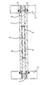
- the drawing shows a cross section through an exposure unit of an exposure device, consisting of metal frame 1, two glass plates 2 Vacuum disks, which are mounted in the metal frame and a spacer frame 3, through which the glass plates are kept at a predetermined distance from one another.
- the space between the glass plates and the spacer frame is sealed against the atmosphere by means of a circumferential V-seal 4 and two circumferential, inflatable hose seals 5 in the vacuum in this space.
- the upper and lower original material 6 according to the invention chemically hardened glass with photographic emulsion - is glued onto the glass plates 2 of the exposure unit using spray adhesive.
- the material 7 to be exposed - for example a printed circuit board - is now placed between the two original materials.
- a vacuum of ⁇ 0.2 bar between the glass plates the original materials are brought into contact with the material to be exposed, which can thereby be exposed.
- the advantages achieved by the invention consist in particular in the fact that the flexibility of the dimensionally stable, chemically hardened glass as the carrier material compensates for these unevenness even with strong pressure on the material, which is often not completely flat, without breaking. Another advantage is that this flexibility makes the handling of this original material much easier due to its breaking strength.
- the material thickness of the carrier material (5 mm in conventional glass masters) can also be reduced to thicknesses of 0.2 mm - 3 mm, preferably 1 mm.
- the UV permeability of the glass is higher and shorter exposure times are achieved.
- the space required for the thinner material when archiving templates is significantly less than with conventional glass masters.
Landscapes
- Engineering & Computer Science (AREA)
- Physics & Mathematics (AREA)
- General Physics & Mathematics (AREA)
- Manufacturing & Machinery (AREA)
- Microelectronics & Electronic Packaging (AREA)
- Exposure And Positioning Against Photoresist Photosensitive Materials (AREA)
- Preparing Plates And Mask In Photomechanical Process (AREA)
- Laminated Bodies (AREA)
Applications Claiming Priority (2)
| Application Number | Priority Date | Filing Date | Title |
|---|---|---|---|
| DE19873712071 DE3712071A1 (de) | 1987-04-09 | 1987-04-09 | Vorlagenmaterial fuer die belichtung von lichtempfindlich beschichteten materialien |
| DE3712071 | 1987-04-09 |
Publications (2)
| Publication Number | Publication Date |
|---|---|
| EP0286018A2 true EP0286018A2 (fr) | 1988-10-12 |
| EP0286018A3 EP0286018A3 (fr) | 1989-07-05 |
Family
ID=6325272
Family Applications (1)
| Application Number | Title | Priority Date | Filing Date |
|---|---|---|---|
| EP88105250A Withdrawn EP0286018A3 (fr) | 1987-04-09 | 1988-03-31 | Masque pour l'exposition d'un matériel revêtu d'une couche photosensible |
Country Status (3)
| Country | Link |
|---|---|
| EP (1) | EP0286018A3 (fr) |
| JP (1) | JPS63261363A (fr) |
| DE (1) | DE3712071A1 (fr) |
Cited By (4)
| Publication number | Priority date | Publication date | Assignee | Title |
|---|---|---|---|---|
| EP0808722A1 (fr) * | 1996-05-21 | 1997-11-26 | Agfa-Gevaert N.V. | Matériel pour la fabrication d'une plaque lithographique ayant un support en verre |
| EP0838723A1 (fr) * | 1996-10-24 | 1998-04-29 | Agfa-Gevaert N.V. | Produit comprenant une couche sur un support en verre |
| EP0875490A1 (fr) * | 1997-04-30 | 1998-11-04 | Agfa-Gevaert N.V. | Méthode de production de verre mince sur un rouleau |
| US6092392A (en) * | 1997-04-30 | 2000-07-25 | Agfa-Gevaert, N.V. | Process for producing thin glass on roll |
Family Cites Families (4)
| Publication number | Priority date | Publication date | Assignee | Title |
|---|---|---|---|---|
| FR434791A (fr) * | 1910-12-06 | 1912-02-13 | Pierre Joseph Taton | Nouveau procédé de tirage photographique industriel |
| US2732298A (en) * | 1952-12-05 | 1956-01-24 | Method of producing a photograph | |
| NL6814882A (fr) * | 1967-12-12 | 1969-06-16 | ||
| US3729316A (en) * | 1970-02-17 | 1973-04-24 | Ibm | Optimized glass photographic mask |
-
1987
- 1987-04-09 DE DE19873712071 patent/DE3712071A1/de not_active Withdrawn
-
1988
- 1988-03-31 EP EP88105250A patent/EP0286018A3/fr not_active Withdrawn
- 1988-04-06 JP JP63083243A patent/JPS63261363A/ja active Pending
Cited By (4)
| Publication number | Priority date | Publication date | Assignee | Title |
|---|---|---|---|---|
| EP0808722A1 (fr) * | 1996-05-21 | 1997-11-26 | Agfa-Gevaert N.V. | Matériel pour la fabrication d'une plaque lithographique ayant un support en verre |
| EP0838723A1 (fr) * | 1996-10-24 | 1998-04-29 | Agfa-Gevaert N.V. | Produit comprenant une couche sur un support en verre |
| EP0875490A1 (fr) * | 1997-04-30 | 1998-11-04 | Agfa-Gevaert N.V. | Méthode de production de verre mince sur un rouleau |
| US6092392A (en) * | 1997-04-30 | 2000-07-25 | Agfa-Gevaert, N.V. | Process for producing thin glass on roll |
Also Published As
| Publication number | Publication date |
|---|---|
| EP0286018A3 (fr) | 1989-07-05 |
| DE3712071A1 (de) | 1988-10-20 |
| JPS63261363A (ja) | 1988-10-28 |
Similar Documents
| Publication | Publication Date | Title |
|---|---|---|
| DE3334993C2 (fr) | ||
| DE3712071A1 (de) | Vorlagenmaterial fuer die belichtung von lichtempfindlich beschichteten materialien | |
| DE1095665B (de) | Verfahren zur fotomechanischen Herstellung von Hochdruckformen aus mehreren Kunststoffschichten | |
| DE3217983C2 (de) | Verfahren zum Herstellen einer Abdeckmaske | |
| DE3033846A1 (de) | Stanzvorrichtung zur justierung von filmen, druckplatten u.dgl. | |
| DE3322703A1 (de) | Film zum chromatischen korrekturlesen | |
| DE1166935B (de) | Verfahren zum Erzeugen von Masken auf Halbleiterkoerpern | |
| US4600298A (en) | Pivotal locking arm for phototool assembly | |
| DE4447264A1 (de) | Verfahren zur Herstellung einer Halbton-Phasenverschiebungsmaske | |
| DE3823463C1 (fr) | ||
| DE2544971A1 (de) | Mehrmetall-druckplatte | |
| DE2748062A1 (de) | Verfahren zur herstellung einer gravierten druckwalze, insbesondere fuer den rotationsdruck | |
| DE2002605A1 (de) | Verfahren zur Herstellung einer abgestuften Schablone | |
| DE3105333A1 (de) | Verfahren zur herstellung von farbfilter-platten | |
| EP0008122B1 (fr) | Procédé de tirage d'une série de diapositives encadrées et dispositif pour la mise en oeuvre de ce procédé | |
| DE511166C (de) | Verfahren zur Herstellung lichtempfindlicher Rollfilme oder Platten | |
| US1724875A (en) | Method of making reproducing plates | |
| DE2119741A1 (de) | Belichtungsvorrichtung | |
| DE3143358A1 (de) | Kopierrahmen zum genauen, visuell-manuellen einrichten und zum halten eines plattenfoermigen werkstuecks | |
| JPS629110Y2 (fr) | ||
| DE2032629A1 (de) | Verfahren und Gebilde zur Herstellung einer Kunststoffplatte | |
| DE487150C (de) | Verfahren zum Herstellen von Strich-, Korn- und Linienraster-Kopier-vorlagen, die auch als Druckplatten Verwendung finden koennen | |
| DE60028975T2 (de) | Verfahren zur Befestigung und Behandlung von Dünnschichtmaterialien | |
| DE2125091C3 (de) | Verfahren zum Herstellen von zusammenpassenden Photokopierschablonen | |
| DE322009C (de) | Verfahren zum Zusammenkopieren von Texten und Bildern mit einem Raster in Chromatleimschichten fuer gleichzeitige Aetzung |
Legal Events
| Date | Code | Title | Description |
|---|---|---|---|
| PUAI | Public reference made under article 153(3) epc to a published international application that has entered the european phase |
Free format text: ORIGINAL CODE: 0009012 |
|
| AK | Designated contracting states |
Kind code of ref document: A2 Designated state(s): AT BE CH DE ES FR GB IT LI NL |
|
| PUAL | Search report despatched |
Free format text: ORIGINAL CODE: 0009013 |
|
| AK | Designated contracting states |
Kind code of ref document: A3 Designated state(s): AT BE CH DE ES FR GB IT LI NL |
|
| 17P | Request for examination filed |
Effective date: 19890608 |
|
| 17Q | First examination report despatched |
Effective date: 19910625 |
|
| STAA | Information on the status of an ep patent application or granted ep patent |
Free format text: STATUS: THE APPLICATION HAS BEEN WITHDRAWN |
|
| 18W | Application withdrawn |
Withdrawal date: 19911011 |