EP0286081A2 - Vektorprozessor mit indirekter Adressierung - Google Patents
Vektorprozessor mit indirekter Adressierung Download PDFInfo
- Publication number
- EP0286081A2 EP0286081A2 EP88105537A EP88105537A EP0286081A2 EP 0286081 A2 EP0286081 A2 EP 0286081A2 EP 88105537 A EP88105537 A EP 88105537A EP 88105537 A EP88105537 A EP 88105537A EP 0286081 A2 EP0286081 A2 EP 0286081A2
- Authority
- EP
- European Patent Office
- Prior art keywords
- vector
- elements
- value
- index
- arithmetic
- Prior art date
- Legal status (The legal status is an assumption and is not a legal conclusion. Google has not performed a legal analysis and makes no representation as to the accuracy of the status listed.)
- Withdrawn
Links
Images


Classifications
-
- G—PHYSICS
- G06—COMPUTING OR CALCULATING; COUNTING
- G06F—ELECTRIC DIGITAL DATA PROCESSING
- G06F15/00—Digital computers in general; Data processing equipment in general
- G06F15/76—Architectures of general purpose stored program computers
- G06F15/80—Architectures of general purpose stored program computers comprising an array of processing units with common control, e.g. single instruction multiple data processors
- G06F15/8053—Vector processors
- G06F15/8061—Details on data memory access
Definitions
- the present invention relates to a vector processor, and in particular, to a vector processor suitable for effecting a vector processing of a binary search necessary in a data base processing.
- N1 stands for a length of a vector D1 including a compare key which is a search request
- N2 is a length of a vector D2 which is an object of the search and is beforehand sorted.
- a vector L indicates the lower limit of the search range
- a vector U indicates the upper limit thereof
- a vector CI designates the center of the search range
- a vector CV(j) denotes a value of each vector element at the center of the search range represented by CI(j) in the search range indicated by D2.
- M stands for a bit series having a length of N1 for storing a compare result. (M is referred to as a mask herebelow.)
- the result of the binary search k is stored in an area for the vector U.
- a counter i of the execution count is reset (step 901) and the vectors L and U are initialized to set the values of the lower and upper limits of the search range (step 902).
- Steps 901 and 902 are effected by use of vector instructions which assign a scalar value to the respective elements of the vector.
- the counter i is then compared with log N2 (step 903). If the counter i is equal to or greater than log N2, the processing is terminated; otherwise, steps 904 to 907 are sequentially executed and then the counter is incremented by one (step 908); thereafter, control returns to the step 903. That is, the steps 904 to 907 are executed log N2 times.
- step 904 a computation of the center position of the search range is achieved for each element (the compare key) of D1.
- This step is effected by use of vector instructions which divide by two a result attained by adding the lower-limit vector L and the upper-limit vector U for each element and store the result in the center position vector CI corresponding to the respective elements.
- each element D2(CI(j)) of D2 located at the center of the search range thus computed in the step 904 is stored in the center value vector CV(j).
- the j-th bit of a mask M is set to 0; otherwise, the j-th bit thereof is set to 1 (step 906).
- the value of CI(j) is stored as the search upper limit U(j) corresponding to D2(j) (step 907).
- the steps 906 and 907 are both accomplished by use of vector instructions.
- the search range stored in the vectors U and L associated with the respective compare keys is reduced to half the original value as a result of the step 907. Consequently, when the steps 904 to 907 are repeatedly executed log N2 times, a search for the elements of D2 equal to the compare key can be completed.
- the center position is set to the upper limit of the search range corresponding to the key value for the next search in the step 907; consequently, even if there exist a plurality of elements of D2 which are equal to the key value D1(j), the position of the element thereof appearing first in D2 is attained as the upper-limit vector U(j).
- the vector including compare keys for the search request in the binary search operation and two vectors of the upper and lower limits representing the search range corresponding to the respective compare keys are separated from each other so as to accomplish the processing separatedly on the respective vectors, which leads to problems that the processing time is increased and that a work area is required.
- the binary search operation is effected by use of six kinds of vector instructions.
- the step 904 requires an add instruction to attain a sum of the vectors U and L and a shift instruction to divide the result by two.
- the step 905 includes a move instruction to load the center value vector CV with a value of the center position of the search range obtained through the step 904.
- the step 906 uses a compare instruction to generate a mask vector so as to rewrite the upper-limit vector and the lower-limit vector.
- Step 907 requires move instructions to rewrite the upper-limit vector U and the lower-limit vector L, respectively.
- the vectors (the vector D1 including a compare key as a search request, the upper-limit vector U, the lower-limit vector L, the sorted vector D2 as an object of the search, the mask vector M, the center position vector CI, and the center value vector CV) as operation objects of the vector instructions above are stored in the main storage.
- the vector processor for example, type M680H Integrated Array Processor of the Hitachi Ltd.
- only read means associated with two channels and write means associated with a channel can be simultaneously used for the main storage.
- each of the vector instructions effecting the binary search operation above requires means to read one or two input vectors and to write an output vector; consequently, it is impossible to increase the processing speed by initiating in a parallel fashion the seven vector instructions effecting the binary search processing so as to execute the vector instructions in an overlapped manner, namely, the steps 904 to 907 of FIG. 9 must be sequentially effected.
- the center position vector CI, the center value vector CV, and the mask vector M are required as work areas for the processing, thus leading to the problems associated with the processing time and the necessary areas.
- a vector processor which comprises first read means for reading as a first collective vector a plurality of vectors such as a vector constituted by elements each indicating a compare key as a search request and a vector constituted by elements each indicating a search range associated with each said compare key, a second read means for generating, from a portion of the elements of said first vector read by said first read means and designated by the search range, information specifying elements of a second vector to be referenced to read said vector elements to be referenced in accordance with the generated information, and arithmetic or logic operation means for effecting an arithmetic or logic operation on the elements of the second vector and the elements of the first vector thus read out, respectively.
- a pipeline operation is performed on two vectors X and Y so as to produce a vector Z.
- Each element of the input vector X includes a four-byte tag part, a four-byte compare key part denoting the search request, and four-byte index parts respectively designating the upper-limit and lower-limit values of the search range.
- Each element of the vector Y including the search object is constituted by a four-byte key.
- the upper limit and the lower limit of the search range are initialized so as to include all elements of the vector Y.
- the binary search operation is conducted as follows. First, the element Xi of the vector X is fetched by use of the first read means. Of the element Xi, the upper-limit and lower-limit values of the index parts denoting the search range are inputted to the position information generate means to generate position information so as to reference the second vector. As a result, the position (to be referred to as the center position j herebelow) of the vector element located at the center of the search range of the vector Y is attained and is then transmitted to the second read means, which then reads the value (to be referred to as the center value Yj herebelow) of the vector element located at the center of the search range of the vector Y and compares the value with the compare key part of the requested element Xi.
- the search range associated with each element of the vector X is reduced to half the original value; consequently, when the instruction is executed log (number of elements of vector Y) times, the value of the upper-limit index can be set to the position of the element of the vector Y, the position identical to the compare key part of each element Xi of the vector X.
- the instruction control circuit 104 sends an operand fetch request via a control signal line 117 to the main storage 107 each a clock signal is received.
- the operand control circuit 106 includes a counter for the vector X comprising a search request. The value of the counter is transmitted via a data path 118 to the address control circuit 105.
- the main storage 107 Upon receiving the fetch request via the control signal line 117, the main storage 107 reads an element X(i) of the vector X by use of a fetch address received via a data path 121a from a read address control circuit 1, 140 in the address control circuit 105.
- the vector element X(i) comprises a tag which is not directly used as an object of the operation, a compare key denoting a search request, and a pair of upper-limit and lower-limit values of a search range in the vector Y corresponding to each compare key.
- partial area specify information indicating a search range in the vector Y is sent via a data path 122 to a circuit 129 for generating information about a fetch element position in a partial area.
- the position information generate circuit 129 constitutes a vector read circuit together with a read address control circuit 2, 141.
- the position information generate circuit 129 divides by two the sum of the counter value for the upper-limit element in the search range of the vector Y and the counter value of the lower-limit element thereof based on the received partial area specify information so as to attain a counter value j (to be referred to as a center element counter value herebelow) of a vector element located at the center of the search range; thereafter, the value of j is sent via a data path 130 to a partial area specify information arithmetic or change circuit 132 and is further transmitted via a data path 124 to the address control circuit 105.
- a counter value j to be referred to as a center element counter value herebelow
- the read address control circuit 2, 141 in the address control circuit 105 generates from the center element counter value j thus received an address of a vector element at the center of the search area in the vector Y as the object of the search and transmits the address via a data path 121b to the main storage 107.
- the main storage 107 reads an element Y(j) of the vector Y based on the fetch request sent from the instruction control circuit 104 via the data path 117 and an operand address sent from the address control circuit 105 via the data path 121b and then sends the element Y(j) via a data path 128 to the partial area specify information change judge circuit 131.
- the change judge circuit 131 functions as an arithmetic unit of the present invention together with a partial area specify information arithmetic or change circuit 132, which will be described later in this specification.
- the change judge circuit 131 compares the compare key value of the element X(i) of the vector X received via the data path 123 with the element Y(j) of the vector Y received via the data path 128 and sends the compare result via a signal line 126 to the partial area specify information arithmetic or change circuit 132, which receives the element X(i) of the vector X via the data path 127 so as to change the search range associated with the element X(i).
- the change operation is carried out according to the result of the comparison accomplished between the compare key value of X(i) received via the signal line 126 and the center value Y(j) of the search range, namely, if the compare key of X(i) is less than Y(j), the center element counter value j received via the data path 130 is employed as the new upper-limit value of the search range so as to change X(i), and then the change result is transmitted as the element Z(i) of the output vector Z via a data path 125 to the main storage 107.
- the center counter value j is adopted as the new lower-limit value of the search range so as to change X(i), and then the change result is transmitted as the element Z(i) of the output vector Z via a data path 125 to the main storage 107.
- the gist of the present invention resides in the following operation. Namely, a compare key value indicating a search request and partial area specify information denoting a search range of each compare key are read in pair as a vector element so as to generate a read address of a vector element located at the center of the search range based on the positions of the upper and lower limits of the search range, and then a vector value of the center of the search range thus read out is compared with the value of the compare key representing the search request so as to change partial area specify information designating the search range. That is, there can be unnecessitated the updated processing conventionally carried out through a plurality of instructions on the vector including the compare key indicating the search request and the vectors of the upper-limit and lower-limit values of the search range.
- the vector instruction includes a bit series comprising 32 bits of which 16 high-order bits 201 represent a kind of the vector instruction.
- An R1 field 202 denotes a 4-bit binary integer and specifies a general purpose register 207 having a number designated by an R1 field in a group of 16 GPR's 103 numbered as C0 to C15.
- an R2 field is used to specify a general purpose register 204 and general purpose registers 205 and 206 subsequent thereto, each having the number equal to the value of the R2 field.
- the GPRs 204 to 206 respectively denote the first addresses of the second operand (Op. 2), the third operand (Op. 3), and the first operand (Op. 1).
- the GPR 207 designates the number of elements of Op. 2.
- the input vectors X and Y are processed as Op. 2 and Op. 3, respectively and the output vector Z is treated as Op. 1. Consequently, in the example of FIG. 8, the first addresses of X, Y, and Z are set to the GPRs 204 to 206, respectively.
- the number of elements of Op. 2 is five, 5 is set to the GPR 207, thereby attaining the result of FIG. 8.
- the length of the input vector Op. 3 as an object of the search is not directly related to the search operation and the number of elements of the output vector Op. 1 is equal to that of elements of the input vector Op. 2, a processing to effect an error check on the number of vector elements is not effected in this embodiment.
- a processing to effect an error check on the number of vector elements is not effected in this embodiment.
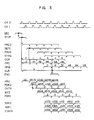
- FIG. 3 is a timing chart of operations of the vector processor of FIG. 1, where Op. 2 and Op. 3 respectively stand for the vectors X and Y of FIG. 8.
- clock signals of two phases CK0 and CK1 are used for establishing synchronization.
- a decoder (DEC) signal 112 notifying the pertinent condition is generated in the instruction control circuit 104.
- FIG. 4 shows the configuration of the instruction control circuit 104.
- the instruction control circuit 104 In response to the DEC signal 112, the instruction control circuit 104 generates a signal STUP 116 instructing the initialization of the respective circuits.
- a hold-type flip-flop circuit 401 is set to indicate that control is passed to the processing of the binary search instruction.
- the operation timing is adjusted by means of a latch circuit 499 and an AND circuit 498.
- the STUP signal 116 is sent to the address control circuit 105 and the operand control circuit 106 for the initialization.
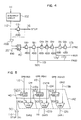
- FIG. 5 shows the configuration of the address control circuit 105.
- the first addresses (a2, a3, and a1) respectively of the second, third, and first operands stored in the GPR's 204 to 206 specified by the instruction register 101 via the signal line 113 are set to the first address registers AR2S 501, AR3S 502, and AR1S 503, respectively, thereby completing the initialization of the address control circuit 105.
- An AND circuit 510 is provided to adjust the timing to set the AR2S 501, AR3S 502, and AR1S 503.
- FIG. 6 shows the configuration of the operand control circuit 106.
- an initial value '0' is set via a selector 601 to an operand counter OCR 602.
- the number of elements of Op. 2 stored in the GPR 207 is transmitted via the data path 114 to an element count register VLR 603 so as to be set thereto in response to the initialize signal STUP 116.
- An AND circuit 612 is provided to adjust the timing to set the element count register VLR 603.
- a fetch request signal FRQ2 for the second operand Op. 2 is delivered from the instruction control circuit 104 via the data path 117a to the main storage 107. Thereafter, the fetch request signal FRQ2 is issued each time a clock signal is received.
- the value of the operand counter OCR 602 is set to '0' in response to the STUP signal 116.
- the counter value is shifted to the left by the shifter 604 so as to be multiplied by the magnitude (16 bytes) of the vector elements of the operand vector Op. 2 and is then delivered via the data path CRI 118a to the address control circuit 105 as an offset value with respect to the vector first address of the vector element indicated by the counter OCR 602 in byte units. (In this case, the pertinent item is the first element of the vector, the value is kept to be '0'.)
- the offset value supplied to the address control circuit 105 is added by the adder 504 to the first address a2 of the input vector Op.
- the main storage 107 Upon receiving the fetch request signal FRQ2 117a, the main storage 107 reads a vector element of Op. 2 from the address indicated by the value stored in the fetch address register AR2 and then stores the attained vector element in the fetch data register FDR2 701 of the main storage 107 (FIG. 7).
- partial area specify information designating the upper and lower limits of the search range (in this example, a pair '04' including a subscript '0' of the vector element located at the upper limit of the partial area of the vector Y and a subscript '4' of the vector element located at the lower limit) is transmitted via the data path 122 to the partial area fetch position information generate circuit 129.
- FIG. 7 shows the configuration of the partial area fetch position information generate circuit 129.
- the subscript values of the upper and lower limits of the search range received via the data path 122 ('0' and '4' in this example) are added to each other in the adder 704 and the result of the addition is shifted by one bit to the right in the shifter 705.
- the subscript of the vector element located at the center of the search range is attained.
- (0 + 4) ⁇ 2 2 results and hence a vector element with a subscript of 2 is set as the vector element at the center of the search range.
- the obtained subscript value is latched into the register 706.
- the value of the subscript assigned to the vector element at the center of the search range is sent via the data path 130 to the partial area specify information arithmetic or change circuit 132; furthermore, the value is multiplied by four in the quardruple circuit 707 and is then multiplied by the length (four bytes) of the element of Op. 3 (vector Y).
- the address control circuit 105 adds by means of the adder 505 the first address of the input vector Op. 3 stored in the first address register AR3S 502 to the offset value in byte units received via the data path 124 so as to send the result of the addition via the data path DAR3 121b to the main storage 107, which in turn loads the result in the fetch address register AR3 thereof ('a3 + 8' is assumed to be the fetch address in this case).
- the process above is accomplished in a period of a clock, namely, after the vector element of the vector Op. 2 is fetched into the fetch data register FDR2, the fetch address of the vector Op. 3 is determined with the subsequent clock CK0.
- a fetch request signal FRQ3 for the vector Op. 3 delayed by two clocks with respect to the fetch request FRQ2 for the vector Op. 2 is transmitted from the instruction control circuit 104 via the data path 117b to the main storage 107.
- the partial area specify information arithmetic or change circuit 132 generates an update result of the search range based on the subscript ('2' in this example) of the element located at the center of the search range received via the data path 130. Namely, the store data registers SDR0 702 and SDR1 703 are loaded with data as follows.
- the range represented by the upper-limit index value Ui (the value of the subscript of the upper-limit element) and the lower-limit index value Li (the value of the subscript of the lower-limit element) in the fetch data register FDR2 is divided by two by the value of the subscript Mi of the element located at the center of the search range received via the data path 130 such that the new search range (represented with a pair of two subscripts Ui and Mi) having the smaller subscript values are stored in the upper-limit and lower-limit index values of SDR0 702, whereas the new search range (represented with a pair of two subscripts Mi and Li) having the greater subscript values are stored in SDR1 703.
- the tag and key values received from the fetch data registers FDR2 via the respective data paths 127a and 127b are set to SDR0 702 and SDR1 703.
- Registers 711 to 713 are provided to adjust the timing of the operation.
- the update results of the search range generated in the two store registers of the partial area specify information arithmetic or change circuit 132 are processed as follows. Namely, depending on the compare result sent via the control line to the store data selector 710 indicating the result of the comparison between the value ('2' in this example) of the compare key designating the search request associated with the vector element Xi and the value ('3' in this example) of the vector element Yj, the value of data to be stored in the main storage 107 is determined.
- the partial area specify information change judge circuit 131 compares by means of the comparator 709 the value of the compare key of the vector element Xi received via the data path 123 with the value of the vector element Yj received via the data path 128 so as to deliver the result of the comparison via the signal line 126 to the partial area specify information arithmetic or change circuit 132. If the value of the compare key of the vector element Xi is smaller than the value of the vector element Yj, the partial area specify information arithmetic or change circuit 132 selects the value of the store register SDR0 702 ('a202' in this example); otherwise, the value of the store register SDR1 703 ('a224' in this example) is selected. (Note that, the value of SDR0 is selected in this case.)
- the value of the vector element Yj located at the center of the search range is loaded in the fetch data register FDR3 708, namely, the store data is determined and is transmitted via the data path 125 to the main storage 107.
- a store request is sent via the signal line 117c to the main storage 107. Since the counter of the vector Op. 1 (vector Z) as the store destination can be assumed to be identical to the input vector Op.
- vector X the value attained by delaying the value ('0' in this example) of the operand counter OCR 602 by three clocks (the operation timing is adjusted by means of the register 611) is shifted by four bits to the left in the shifter 605 so as to be converted into an offset value (kept remained to be '0' in this example) with respect to the first address of the vector Op. 1 (vector Z) in byte units.
- the resultant value is sent via the data path CRID 118b to the address control circuit 105.
- vector Z is added to the offset value ('0' in this example) in byte units sent via the data path CRID 118b in the adder 506, and the result of the addition is then transmitted as a store address via the data path DAR1 121c to the store address register of the main storage 107.
- the main storage 107 Upon receiving the store request signal STRQ 117c, the main storage 107 stores the value ('a202' in this example) received via the data path 125 in a location indicated by the store address register.
- the value of the operand counter OCR 602 is incremented by one and becomes to be '1'.
- the address registers associated with Op. 2 and Op. 1 are respectively updated to indicate the next processing elements of the vectors X and Z, respectively. Thereafter, each time the fetch request FRQ2 117a is transmitted, the binary search processing is similarly accomplished on the second and subsequent vector elements of the input vector Op. 2.
- the operand counter OCR 602 indicates the last element (the OCR content is '4' in this example) of the input vector Op. 2 (vector X) as a result of the processing thus achieved, a value attained by adding one to the content of the OCR 602 is transmitted via the data path 606.
- the value here matches with the value held in the vector count register VLR 607 in the operand control circuit 106.
- the matching condition is detected by the comparator CMP 607 and then the instruction processing end signal END is sent via the signal line 120 to the instruction control circuit 104, which in turn resets the flip-flop circuit 401 indicating that the binary search operation is being processed.
- the fetch requests FRQ2 117a and FRQ3 117b and the store request STRQ 117c are terminated, thereby ending the processing of the binary search operation.
- the vector Z is attained as the first operand vector of the instruction in the main storage 107.
- the vector Z includes elements each comprising a tag, a key, and values of subscripts of elements respectively located at the upper and lower limits of a partial area of the vector Y where a vector element having a value equal to the value of the key is considered to exist. Assuming that the vector Y includes N elements, if this instruction is repeatedly executed log2 N times, the search range converges to a single vector element.
- a vector operation is to be executed in a vector processor having two read means on three input vectors including a first vector comprising first values each indicating an object of the operation, a second vector including address values for second values to be used as objects of the operation, and a third vector including said second values wherein the vector operation is achieved for the respective corresponding vector elements of the first and second vectors; elements of the first and second vectors are read by first read means for the corresponding elements thereof, second read means is initiated depending on the value of the element of the second vector so as to read an element of the third vector, thereby executing an operation with the element of the first vector beforehand read out.
- the overall processing is subdivided into two processing parts including a processing in which an element of the third vector is referenced and moved according to an address value of the second vector so as to temporarily generate a vector in a work area and a processing in which an operation is achieved between the vector thus temporarily generated in the work area and the first vector. Furthermore, since the number of read means is limited to two, the two processing procedures above cannot be carried out in an overlapped fashion.
- the two processing procedures are combined into a processing; moreover, the processing is achieved in an overlapped fashion, which enables the processing speed to be increased.
- circuits executing vector instructions associated with a binary search processing the present invention is not restricted by those circuits, namely, various variations thereof can be included in the present invention without departing from the scope and spirit of the present invention.
Landscapes
- Engineering & Computer Science (AREA)
- Computer Hardware Design (AREA)
- Theoretical Computer Science (AREA)
- Computing Systems (AREA)
- Physics & Mathematics (AREA)
- General Engineering & Computer Science (AREA)
- General Physics & Mathematics (AREA)
- Complex Calculations (AREA)
- Information Retrieval, Db Structures And Fs Structures Therefor (AREA)
Applications Claiming Priority (2)
| Application Number | Priority Date | Filing Date | Title |
|---|---|---|---|
| JP84735/87 | 1987-04-08 | ||
| JP62084735A JPS63251835A (ja) | 1987-04-08 | 1987-04-08 | ベクトル処理装置 |
Publications (2)
| Publication Number | Publication Date |
|---|---|
| EP0286081A2 true EP0286081A2 (de) | 1988-10-12 |
| EP0286081A3 EP0286081A3 (de) | 1990-08-08 |
Family
ID=13838952
Family Applications (1)
| Application Number | Title | Priority Date | Filing Date |
|---|---|---|---|
| EP88105537A Withdrawn EP0286081A3 (de) | 1987-04-08 | 1988-04-07 | Vektorprozessor mit indirekter Adressierung |
Country Status (3)
| Country | Link |
|---|---|
| US (1) | US5010483A (de) |
| EP (1) | EP0286081A3 (de) |
| JP (1) | JPS63251835A (de) |
Cited By (1)
| Publication number | Priority date | Publication date | Assignee | Title |
|---|---|---|---|---|
| EP0479235A3 (en) * | 1990-10-02 | 1992-09-09 | Nec Corporation | Vector processing device comprising a reduced amount of hardware |
Families Citing this family (3)
| Publication number | Priority date | Publication date | Assignee | Title |
|---|---|---|---|---|
| US5261090A (en) * | 1990-06-12 | 1993-11-09 | At&T Bell Laboratories | Search arrangement adapted for data range detection |
| JP2665111B2 (ja) * | 1992-06-18 | 1997-10-22 | 日本電気株式会社 | ベクトル処理装置 |
| US7299338B2 (en) * | 2002-12-04 | 2007-11-20 | Agere Systems Inc. | Vector indexed memory unit and method |
Family Cites Families (8)
| Publication number | Priority date | Publication date | Assignee | Title |
|---|---|---|---|---|
| US3267433A (en) * | 1962-08-24 | 1966-08-16 | Ibm | Computing system with special purpose index registers |
| JPS5725069A (en) * | 1980-07-21 | 1982-02-09 | Hitachi Ltd | Vector data processing equipment |
| JPS58146969A (ja) * | 1982-02-26 | 1983-09-01 | Toshiba Corp | インデツクス限定連続演算ベクトルプロセツサ |
| JPS6069746A (ja) * | 1983-09-26 | 1985-04-20 | Fujitsu Ltd | ベクトル・デ−タ処理装置の制御方式 |
| JPH077385B2 (ja) * | 1983-12-23 | 1995-01-30 | 株式会社日立製作所 | データ処理装置 |
| JPS61210477A (ja) * | 1984-05-25 | 1986-09-18 | Hitachi Ltd | ベクトル型連想メモリシステム |
| US4745547A (en) * | 1985-06-17 | 1988-05-17 | International Business Machines Corp. | Vector processing |
| JPS62115571A (ja) * | 1985-11-15 | 1987-05-27 | Fujitsu Ltd | ベクトルアクセス制御方式 |
-
1987
- 1987-04-08 JP JP62084735A patent/JPS63251835A/ja active Pending
-
1988
- 1988-04-07 US US07/178,913 patent/US5010483A/en not_active Expired - Fee Related
- 1988-04-07 EP EP88105537A patent/EP0286081A3/de not_active Withdrawn
Cited By (1)
| Publication number | Priority date | Publication date | Assignee | Title |
|---|---|---|---|---|
| EP0479235A3 (en) * | 1990-10-02 | 1992-09-09 | Nec Corporation | Vector processing device comprising a reduced amount of hardware |
Also Published As
| Publication number | Publication date |
|---|---|
| EP0286081A3 (de) | 1990-08-08 |
| US5010483A (en) | 1991-04-23 |
| JPS63251835A (ja) | 1988-10-19 |
Similar Documents
| Publication | Publication Date | Title |
|---|---|---|
| US5608887A (en) | Method of processing data strings | |
| EP0149213B1 (de) | Vektorprozessor | |
| US4679140A (en) | Data processor with control of the significant bit lengths of general purpose registers | |
| US4408275A (en) | Data processing system with data cross-block-detection feature | |
| JPH03108042A (ja) | 多重仮想空間アドレス制御方法および計算機システム | |
| US5761521A (en) | Processor for character strings of variable length | |
| US4317170A (en) | Microinstruction controlled data processing system including micro-instructions with data align control feature | |
| US4739470A (en) | Data processing system | |
| US4541047A (en) | Pipelined data processing system | |
| US4773006A (en) | Vector operation designator | |
| US4933839A (en) | Vector processor | |
| EP0163279B1 (de) | Vektorverarbeitungsgerät | |
| EP0286081A2 (de) | Vektorprozessor mit indirekter Adressierung | |
| US4384343A (en) | Firmware controlled search and verify apparatus and method for a data processing system | |
| US4309753A (en) | Apparatus and method for next address generation in a data processing system | |
| US5124910A (en) | Microprogram control apparatus for generating a branch condition signal to be designated by a micro-branch instruction | |
| JP2580396B2 (ja) | パイプラインにおける分岐命令制御方式 | |
| US5479620A (en) | Control unit modifying micro instructions for one cycle execution | |
| US5291615A (en) | Instruction pipeline microprocessor | |
| US4924377A (en) | Pipelined instruction processor capable of reading dependent operands in parallel | |
| GB1602421A (en) | Processors for data processing systems | |
| EP0270125B1 (de) | Fliessbandsteuerungssystem | |
| JPS59114677A (ja) | ベクトル処理装置 | |
| US5377335A (en) | Multiple alternate path pipelined microsequencer and method for controlling a computer | |
| US5600842A (en) | Microprogram controller for controlling readout of a microprogram stored in multiple storage areas |
Legal Events
| Date | Code | Title | Description |
|---|---|---|---|
| PUAI | Public reference made under article 153(3) epc to a published international application that has entered the european phase |
Free format text: ORIGINAL CODE: 0009012 |
|
| AK | Designated contracting states |
Kind code of ref document: A2 Designated state(s): DE GB |
|
| PUAL | Search report despatched |
Free format text: ORIGINAL CODE: 0009013 |
|
| AK | Designated contracting states |
Kind code of ref document: A3 Designated state(s): DE GB |
|
| 17P | Request for examination filed |
Effective date: 19900813 |
|
| 17Q | First examination report despatched |
Effective date: 19930323 |
|
| STAA | Information on the status of an ep patent application or granted ep patent |
Free format text: STATUS: THE APPLICATION HAS BEEN WITHDRAWN |
|
| 18W | Application withdrawn |
Withdrawal date: 19930802 |