EP0286123A2 - Festkörper-Bildabtaster mit Hochgeschwindigkeitsverschluss und Verfahren zur Erzielung einer hohen Verschlussgeschwindigkeit in einem Festkörper-Bildabtaster - Google Patents
Festkörper-Bildabtaster mit Hochgeschwindigkeitsverschluss und Verfahren zur Erzielung einer hohen Verschlussgeschwindigkeit in einem Festkörper-Bildabtaster Download PDFInfo
- Publication number
- EP0286123A2 EP0286123A2 EP88105640A EP88105640A EP0286123A2 EP 0286123 A2 EP0286123 A2 EP 0286123A2 EP 88105640 A EP88105640 A EP 88105640A EP 88105640 A EP88105640 A EP 88105640A EP 0286123 A2 EP0286123 A2 EP 0286123A2
- Authority
- EP
- European Patent Office
- Prior art keywords
- field
- charges
- transferred
- pulse
- section
- Prior art date
- Legal status (The legal status is an assumption and is not a legal conclusion. Google has not performed a legal analysis and makes no representation as to the accuracy of the status listed.)
- Granted
Links
Images





Classifications
-
- H—ELECTRICITY
- H04—ELECTRIC COMMUNICATION TECHNIQUE
- H04N—PICTORIAL COMMUNICATION, e.g. TELEVISION
- H04N25/00—Circuitry of solid-state image sensors [SSIS]; Control thereof
- H04N25/70—SSIS architectures; Circuits associated therewith
- H04N25/71—Charge-coupled device [CCD] sensors; Charge-transfer registers specially adapted for CCD sensors
- H04N25/715—Charge-coupled device [CCD] sensors; Charge-transfer registers specially adapted for CCD sensors using frame interline transfer [FIT]
-
- H—ELECTRICITY
- H04—ELECTRIC COMMUNICATION TECHNIQUE
- H04N—PICTORIAL COMMUNICATION, e.g. TELEVISION
- H04N23/00—Cameras or camera modules comprising electronic image sensors; Control thereof
- H04N23/10—Cameras or camera modules comprising electronic image sensors; Control thereof for generating image signals from different wavelengths
- H04N23/12—Cameras or camera modules comprising electronic image sensors; Control thereof for generating image signals from different wavelengths with one sensor only
-
- H—ELECTRICITY
- H04—ELECTRIC COMMUNICATION TECHNIQUE
- H04N—PICTORIAL COMMUNICATION, e.g. TELEVISION
- H04N25/00—Circuitry of solid-state image sensors [SSIS]; Control thereof
- H04N25/50—Control of the SSIS exposure
- H04N25/53—Control of the integration time
Definitions
- the present invention relates to a solid-state imaging device such as a charge-coupled device (CCD) and, more particularly, to a solid-state imaging device having a high-speed shutter function and a method of realizing the high-speed function in the solid-state imaging device.
- a solid-state imaging device such as a charge-coupled device (CCD)
- CCD charge-coupled device
- a solid-state imaging device such as a CCD is a comparatively recent development, and a color video camera incorporating this device is now commercially available.
- the charge storage time of the photosensitive section of the device corresponds to the shutter time of a still photography camera, and is normally set to 1/60 sec.
- a typical FIT type CCD comprises photosensitive and high-speed vertical transfer sections which constitute an imaging section, a field memory which serves as a storage section, and a horizontal transfer section. This type of CCD operates in the following manner:
- the charges in the photosensitive section are shifted in response to the discharge field shift pulse, after which the charges read in response to the signal read field shift pulse are stored in the storage section.
- the time interval between the discharge and signal read field shift pulses constitutes the shutter speed. By selecting this time interval, a specified shutter speed can be set.
- a one-field image can be obtained by a high-speed shutter operation.
- a two-field (i.e., one-frame) image constituted by odd- and even-numbered fields is obtained so as to improve the vertical resolution.
- two shutter operations are required. If two shutter operations are performed in the above-described camera, the time interval between first and second shutter operations is 1/60 sec. Accordingly, although the one-field image can be obtained by the high-speed operation, the one-frame image corresponds to an image obtained by repeating the high-speed operation twice at a time interval of 1/60 sec. Therefore, when the motion of an object to be imaged is fast, flicker is caused and the resultant image becomes poor.
- an object of the present invention to provide a solid-state imaging device the shutter of which can operate at high-speed, so that one-frame images of excellent vertical resolution can be obtained, which are free from flicker even when the object being imaged is in rapid motion, another object of the present invention being to provide a method of realizing the above.
- a solid-state imaging device having high-speed shutter function comprises: a photosensitive section for storing charges corresponding to an amount of received light and a period of time during which the light is received; a high-speed transfer section to which the charges stored in the photosensitive section are simultaneously transferred in response to field shift pulses which include a discharge field shift pulse and first and second signal reading field shift pulses; a field memory to which are transferred, in units of lines and at a high speed, the charges transferred to the high-speed transfer section, the field memory storing the transferred charges; a line transfer section to which the charges stored in the field memory are transferred in unit of lines; and driver means for successively generating the discharge field shift pulse, and the first and second signal read field shift pulses at equal time intervals for one shutter operation, such that a light storage time in the photosensitive section, between generation of the discharge field shift pulse and generation of the first signal read field shift pulse, coincides with a light storage time, also in the photosensitive section, between generation of the
- a solid-state imaging device having a high-speed shutter function comprises: a photosensitive section for storing charges corresponding to an amount of received light and a period of time during which the light is received; a high-speed transfer section to which the charges stored in the photosensitive section are simultaneously transferred in response to field shift pulses which include a discharge field shift pulse and first and second signal read field shift pulses; a first field memory to which are transferred, in units of lines and at a high speed, the charges transferred to the high-speed transfer section, the first field memory storing the transferred charges; a second field memory to which the charges stored in the first field memory are transferred in units of lines and at a high speed, the second field memory storing the transferred charges; a line transfer section to which the charges stored in the second field memory are transferred in units of lines; and driver means for generating a drive pulse for causing the high-speed transfer section to transfer to the field memory, in units of lines, the charges transferred to the high-speed transfer section, and
- a method of realizing a high-speed shutter function in a solid-state imaging device comprises: a first step of supplying a discharge field shift pulse for discharging charges stored in accordance with an amount of received light and a period of time during which the light is received; a second step of supplying a first signal read field shift pulse; a third step of storing charges, which are stored after the first step, in a first storage means, in response to the first signal read field shift pulse; a fourth step of supplying a second signal read field shift pulse, the second signal read field shift pulse being supplied at a timing such that a time interval between supply of the discharge field shift pulse and supply of the first signal read field shift pulse coincides with a time interval between supply of the first signal read field shift pulse and supply of the second signal read field shift pulse; a fifth step of storing charges, which are stored after the third step, in a second storage means, in response to the second signal read field shift pulse; a sixth step of transferring the charges, which are stored in the first storage means
- Fig. 1 shows an arrangement of an embodiment of the present invention.
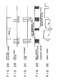
- Figs. 2A to 2E are timing charts for explaining operations of the embodiment.
- driver 14 When shutter 12 for photographing is operated, driver 14 successively generates discharge field shift pulse P s and first and second signal read field shift pulses P1 and P2 for one photographing operation, and supplies them to CCD 16 serving as a solid-state imaging device. Time intervals for supplying field shift pulses P s , P1, and P2 are set to be equal.
- CCD 16 is of an interline transfer type, and is periodically operated in a normal operation mode in accordance with vertical blanking pulses.
- CCD 16 comprises photosensitive and vertical high-speed transfer sections 18 and 20 constituting an imaging section, field memory 22 as a storage section, horizontal transfer section 24, and output circuit 26.
- Photosensitive section 18 includes, e.g., 500 vertical and 200 horizontal pixels (photodiodes).
- CCD 16 In CCD 16, a gate (not shown) arranged between photosensitive section 18 and high-speed transfer section 20 is enabled in response to first discharge field shift pulse P s . As a result, charges in photosensitive section 18 are simultaneously transferred to high-speed transfer section 20. The charges in high-speed transfer section 20 are discharged upward in a direction indicated by arrow ⁇ in Fig. 1 at a high speed during period t1 in accordance with clocks ( ⁇ V1 , ⁇ V2 , ⁇ V3 , and ⁇ V4 ) supplied from driver 14. During this period, image charges are stored in photosensitive section 18.
- first signal read field shift pulse P1 is output from driver 14.
- field shift pulse P1 signal electric charges of odd- and even-numbered pixels in photosensitive section 18 are added to each other, and the resultant charges are transferred to high-speed transfer section 20.
- the charges transferred to high-speed transfer section 20 are transferred downward in a direction indicated by arrow ⁇ in Fig. 1, i.e., transferred to field memory 22 at a high speed within period t2.
- the next image charges are stored in photosensitive section 18 during period t2.
- second signal read field shift pulse P2 is supplied from driver 14.
- signal charges of the next field i.e., of even- and odd-numbered pixels are added to each other.
- the resultant charges are simultaneously transferred to high-speed transfer section 20.
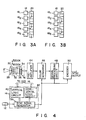
- Figs. 3A and 3B are views for explaining a method of adding images of the first and second field to each other.
- signals of odd- and even-numbered pixels in photosensitive section 18 are added to each other in response to first signal read field shift pulse P1. More specifically, sum signals corresponding to charges of pixels 181 + 182, 183 + 184, ..., are stored in high-speed transfer section 20.
- signals of even- and odd-numbered pixels in photosensitive section 18 are added to each other, as shown in Fig. 3B. More specifically, sum signals corresponding to charges of pixels 182 + 183, 184 + 185, ..., are stored in high-speed transfer section 20.
- image charges of the first and second fields are respectively present in field memory 22 and high-speed transfer section 20.
- the image of the first field is read during period T1 through horizontal transfer section 24 in a manner similar to a normal television scanning operation, and the image charges of the second field are transferred to field memory 22 at a high speed during period T2. Then, the image of the second field is read through horizontal transfer section 24 during period T3 in a manner similar to a normal television scanning operation, thereby obtaining a one-frame image.
- the image includes signals of the first (odd-numbered) field, and signals of the second (even-numbered) field.
- the signals of the respective fields are obtained at equal shutter intervals.
- a time lag between the first and second fields is very small, as shown in Fig. 2C.
- a shutter time i.e., a shutter speed can be arbitrarily set by adjusting the time intervals between field shift pulses P s , P1, and P2.
- Fig. 4 shows an arrangement of a color video camera using a solid-state imaging device according to the present invention.
- Light passes through zoom lens 28 of 3x magnification is focused onto the imaging section in CCD 16 serving as a solid-state imaging device with color filter array 36 through color temperature converting filter 30, color correction filter 32, and optical low-pass filter (LPF) 34.
- LPF optical low-pass filter
- Driver 14 includes sync signal generator 38, vertical logic circuit 40, and horizontal logic circuit 42.
- Vertical and horizontal logic circuits 40 and 42 generate various pulses necessary for the operation of CCD 16 using various types of pulse signals supplied from sync signal generator 38, and supplies them to CCD 16.
- An output signal from CCD 16 is amplified by preamplifier 44, and then separated by color separator 46 into three primary color signals, namely the red (R), green (G), and blue (B) signals. These primary color signals are subjected to signal processing required for a normal color camera such as gamma correction and white clip in signal processing circuit 48, and then supplied to encoder 50. Encoder 50 generates luminance and chrominance signals from the input signals, and mixes them to generate and output a standard NTSC signal.
- Sync signal generator 38 generates timing pulses (F Ss , F S1 , F S2 , F V1 , F V2 , F V3 , F V4 , HP, and VP) necessary for the vertical and horizontal drive operations, and supplies them to vertical and horizontal logic circuits 40 and 42.
- Vertical logic circuit 40 generates each pulse waveform ( ⁇ V1 , ⁇ V2 , ⁇ V3 , ⁇ V4 , ⁇ F1 , ⁇ F2 , ⁇ F3 , and ⁇ F4 ) necessary for vertical transfer operations in imaging and storage sections 52 and 54 in CCD 16.
- Horizontal logic circuit 42 generates each pulse waveform ( ⁇ H1 , ⁇ H2 , and ⁇ RS ) necessary for horizontal transfer.
- the waveforms necessary for horizontal transfer are two-phase drive waveforms ( ⁇ H1 and ⁇ H2 ) shown in Figs. 6A and 6B, and a reset pulse waveform ( ⁇ RS ) shown in Fig. 6C to be supplied to output circuit 26.
- ⁇ H1 and ⁇ H2 two-phase drive waveforms
- ⁇ RS reset pulse waveform
- Waveform ⁇ V shown in Fig. 7C is equivalent to each of pulse waveforms ⁇ V1 , ⁇ V2 , ⁇ V3 , and ⁇ V4 supplied to imaging section 52.
- reference symbol S denotes a discharge period, in which four-phase pulse waveforms shown in Fig. 8 are output.
- Reference symbol I denotes a transfer period of signals, in which four-phase pulse waveforms shown in Fig. 9 are output.
- FIG. 7D is equivalent to each of pulse waveforms ⁇ F1 , ⁇ F2 , ⁇ F3 , and ⁇ F4 .
- Fig. 7D four-phase pulse waveforms shown in Fig. 10 are output in a period denoted by reference symbol I.
- the discharge period of unnecessary charges and the transfer period of signals are present in imaging section 52.
- the phases of four-phase waveforms change. This determines a transfer direction, i.e., either of the upward and downward directions indicated by arrows ⁇ and ⁇ in Fig. 1.
- pulse signal ⁇ F to be supplied to storage section 54 becomes a four-phase high-speed transfer pulse, and therefore the signal charges are taken into storage section 54 at a high speed, as shown in Figs. 7D and Fig. 10. More specifically, as shown in Fig. 10, in accordance with the timing of applying a voltage of 5V which is shifted in the order of ⁇ F1 ⁇ ⁇ F2 ⁇ F3 ⁇ ⁇ F4 , the signal charges are transferred to storage section 54.
- a one-line signal is added every 1H, and the signals are shifted from storage section 54 to horizontal transfer section 24. This operation is performed such that the four-phase waveform having one period is generated and a nonoperative state is temporarily set.
- field shift pulses (P s , P1, and P2) are supplied to enable the gate (not shown) arranged between photosensitive section 18 and high-speed transfer section 20.
- signals are shifted from photosensitive section 18 to high-speed transfer section 20. That is, field shift pulses P s , P1, and P2 are required to shift the signals from photosensitive section 18 to high-speed transfer section 20.
- these field shift pulses are superposed on pulse waveforms ⁇ V1 and ⁇ V3 , and supplied from vertical logic circuit 40 to imaging section 52.
- pulse waveform ⁇ V3 is set at +5V
- the signal charge at the electrode to which pulse waveform ⁇ V2 is supplied is added to the signal charge at the electrode to which pulse waveform ⁇ V3 is supplied. That is, as shown in Fig. 3A, a charge of an odd-numbered pixel in photosensitive section 18 is shifted through the electrodes to which pulse waveforms ⁇ V1 and ⁇ V2 are supplied and added to a signal charge of an even-numbered pixel at the electrode to which pulse waveform ⁇ V3 is supplied.
- pulse waveform ⁇ V1 is set at +5 V
- the signal charge at the electrode to which pulse waveform ⁇ V4 is supplied is added to the signal charge at the electrode to which pulse waveform ⁇ V1 is supplied. That is, as shown in Fig. 3B, a charge of an even-numbered pixel is shifted through the electrodes to which pulse waveforms ⁇ V3 and ⁇ V4 , and added to a signal charge of an odd-numbered pixel at the electrode to which pulse waveform ⁇ V1 is supplied.
- a high-speed shutter operation can be performed, and a one-frame image having excellent vertical resolution can be obtained.
- a signal for a still picture is obtained using a normal video camera, if an object moves, flicker is caused because a shutter is closed at an interval of 1/60 sec between odd- and even-numbered fields. For this reason, a complete one-frame image cannot be obtained.
- a still image with an excellent vertical resolution can be obtained.
- a variable-speed shutter is employed, a one-frame still image can be obtained at an arbitrary speed.
- signals of the second field are stored in high-speed transfer section 20. Therefore, it is preferable for the area of high-speed transfer section 20 to be completely shielded from light. More specifically, since a time lag is present between the period when signals of the first field are read and the period when signals of the second field are read, the signals read later are to be stored in high-speed transfer section 20 for a longer period of time corresponding to the time lag. For this reason, if this area is not completely shielded from light, a difference in a smear amount is caused.
- the area of high-speed transfer section 20 is completely shield from light.
- a field memory may be added so that the signals can be stored therein in place of high-speed transfer section 20.
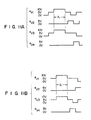
- Fig. 12 shows an arrangement of another embodiment related to the above case.
- Figs. 13A to 13E are timing charts of the embodiment.
- two field memories (denoted by reference numerals 221 and 222 in Fig. 12) are used as a storage section.
- CCD 16 ⁇ With such an arrangement, charges stored in photosensitive section 18 are simultaneously transferred to high-speed transfer section 20 in response to first field shift pulse P s .
- the charges in high-speed transfer section 20 are discharged at a high speed in a direction indicated by arrow ⁇ in Fig. 12 during period t1 in accordance with a clock supplied from driver 14. Image charges are stored in photosensitive section 18 within this period.
- first signal read field shift pulse P1 is output from driver 14.
- signal charges of odd- and even-numbered pixels in photosensitive section 18 are added to each other, and the resultant signals are transferred to high-speed transfer section 20.
- the charges transferred to high-speed transfer section 20 are transferred in a direction indicated by arrow ⁇ in Fig. 12, i.e., to field memory 221 at a high speed within period t2.
- the next image charges are stored in photosensitive section 18.
- driver 14 supplies second signal read field shift pulse P2.
- signal charges of the next field i.e., of even- and odd-numbered pixels, and simultaneously transferred to high-speed transfer section 20.
- the charges in high-speed transfer section 20 are transferred to field memory 221 at a high speed within period t2.
- the charges which have been stored in field memory 221 are transferred field memory 222 of the next stage.
- the image charges of the first and second fields are respectively present in field memories 221 and 222.
- the image (the contents in field memory 222) of the first field is read in period T1 through horizontal transfer section 24 in a manner similar to the normal television scanning operation.
- the contents in field memory 221 are transferred to field memory 222.
- the image (the contents in field memory 222) of the second field is read in a manner similar to the normal television scanning operation, thereby obtaining a one-frame image.
- This image includes the signals of the first (odd-numbered) and second (even-numbered) fields. The signals of the respective fields are obtained at equal shutter intervals.
- a time lag between the first and second fields is very small, as shown in Fig. 13C.
- a shutter time i.e., a shutter speed can be arbitrarily set by adjusting the time intervals between field shift pulses P s , P1, and P2.
- This embodiment is characterized in that signals of the first and second fields are simultaneously transferred to a plurality of field memories, i.e., field memories 221 and 222, respectively. That is, the signals of the first and second fields are respectively transferred to the first and second field memories so as not to cause a time lag between dwelling times of the charges in high-speed transfer section 20.
- the field memory area is completely shielded from light, and smear can be prevented.
- the two storage sections are arranged between the imaging section and the horizontal transfer section.
- the present invention is not limited to this arrangement.
- a pair of storage and horizontal transfer sections may be arranged on each of upper and lower portions of the imaging section.
- the number of storage sections is not limited to two.
- first, second, and third storage sections may be arranged so that signals having red (R), green (G), and blue (B) color information are respectively stored in the first, second, and third storage sections. With this arrangement, the R, G, and B color image signals without smear can be obtained.
- a high-speed shutter operation can be performed, and a one-frame image with an excellent vertical resolution can be obtained.
- flicker is caused because a shutter is closed at an interval of 1/60 sec between odd- and even-numbered fields. Therefore, a complete one-frame image cannot be obtained.
- a still image with an excellent vertical resolution can be obtained.
- one-frame still image can be obtained at an arbitrary speed. Moreover, differences in signal level between the fields are not produced, and hence an image signal with excellent quality can be obtained.
Landscapes
- Engineering & Computer Science (AREA)
- Multimedia (AREA)
- Signal Processing (AREA)
- Transforming Light Signals Into Electric Signals (AREA)
Applications Claiming Priority (4)
| Application Number | Priority Date | Filing Date | Title |
|---|---|---|---|
| JP88174/87 | 1987-04-10 | ||
| JP8817487 | 1987-04-10 | ||
| JP62088176A JP2549653B2 (ja) | 1987-04-10 | 1987-04-10 | 固体撮像素子カメラ |
| JP88176/87 | 1987-04-10 |
Publications (3)
| Publication Number | Publication Date |
|---|---|
| EP0286123A2 true EP0286123A2 (de) | 1988-10-12 |
| EP0286123A3 EP0286123A3 (en) | 1989-05-31 |
| EP0286123B1 EP0286123B1 (de) | 1992-12-30 |
Family
ID=26429599
Family Applications (1)
| Application Number | Title | Priority Date | Filing Date |
|---|---|---|---|
| EP88105640A Expired - Lifetime EP0286123B1 (de) | 1987-04-10 | 1988-04-08 | Festkörper-Bildabtaster mit Hochgeschwindigkeitsverschluss und Verfahren zur Erzielung einer hohen Verschlussgeschwindigkeit in einem Festkörper-Bildabtaster |
Country Status (4)
| Country | Link |
|---|---|
| US (1) | US4831453A (de) |
| EP (1) | EP0286123B1 (de) |
| KR (1) | KR920003655B1 (de) |
| DE (1) | DE3877034T2 (de) |
Cited By (13)
| Publication number | Priority date | Publication date | Assignee | Title |
|---|---|---|---|---|
| EP0365000A1 (de) * | 1988-10-21 | 1990-04-25 | Nec Corporation | CCD-Bildsensor mit vertikaler Überlauf-Senke |
| EP0505117A3 (en) * | 1991-03-16 | 1993-08-11 | Kabushiki Kaisha Toshiba | Color imaging system with integration time control |
| EP0561633A3 (en) * | 1992-03-18 | 1993-11-24 | Sony Corp | Solid-state imaging apparatus |
| WO1995018506A1 (fr) * | 1993-12-30 | 1995-07-06 | Thomson-Csf | Procede d'adressage progressif d'un dispositif a transfert de charges et dispositif de prise de vue utilisant ce procede |
| EP0599200A3 (de) * | 1992-11-20 | 1995-08-09 | Matsushita Electric Industrial Co Ltd | Festkörperbildaufnahmevorrichtung und Verfahren zu ihrem Betrieb. |
| EP1073262A3 (de) * | 1999-07-30 | 2001-12-12 | Eastman Kodak Company | Bildsensor mit hoher Auslesegeschwindigkeit |
| US20110075008A1 (en) * | 2009-09-30 | 2011-03-31 | Border John N | Methods for capturing and reading out images from an image sensor |
| US8194164B2 (en) | 2009-09-30 | 2012-06-05 | Truesense Imaging, Inc. | Methods for capturing and reading out images from an image sensor |
| US8194166B2 (en) | 2009-09-30 | 2012-06-05 | Truesense Imaging, Inc. | Methods for capturing and reading out images from an image sensor |
| US8194165B2 (en) | 2009-09-30 | 2012-06-05 | Truesense Imaging, Inc. | Methods for capturing and reading out images from an image sensor |
| US8279317B2 (en) | 2009-09-30 | 2012-10-02 | Truesense Imaging, Inc. | Methods for capturing and reading out images from an image sensor |
| US8279316B2 (en) | 2009-09-30 | 2012-10-02 | Truesense Imaging, Inc. | Methods for capturing and reading out images from an image sensor |
| US8294803B2 (en) | 2009-09-30 | 2012-10-23 | Truesense Imaging, Inc. | Methods for capturing and reading out images from an image sensor |
Families Citing this family (28)
| Publication number | Priority date | Publication date | Assignee | Title |
|---|---|---|---|---|
| US4972267A (en) * | 1988-06-14 | 1990-11-20 | Fuji Photo Film Co., Ltd. | Still-video camera for eliminating dark current differences |
| US5031048A (en) * | 1988-08-09 | 1991-07-09 | Minolta Camera Kabushiki Kaisha | Electric shutter control device for use in a still video camera, for example, and a method of controlling same |
| US5043821A (en) * | 1988-08-31 | 1991-08-27 | Canon Kabushiki Kaisha | Image pickup device having a frame-size memory |
| US5113365A (en) * | 1989-05-16 | 1992-05-12 | Massachusetts Institute Of Technology | Method and charge coupled apparatus for algorithmic computations |
| JP2818214B2 (ja) * | 1989-08-31 | 1998-10-30 | 株式会社東芝 | 固体撮像装置 |
| JP2853216B2 (ja) * | 1989-11-09 | 1999-02-03 | 日本電気株式会社 | 固体撮像装置 |
| FR2655504B1 (fr) * | 1989-12-01 | 1992-02-21 | Thomson Csf | Procede et dispositif de compression de debit pour camera visiophonique munie d'une matrice photosensible a transfert de charges et systeme de transmission d'images correspondant. |
| JP2760639B2 (ja) * | 1990-07-04 | 1998-06-04 | 株式会社東芝 | 固体撮像装置およびその駆動方法 |
| US5734424A (en) * | 1990-08-08 | 1998-03-31 | Canon Kabushiki Kaisha | Image pickup apparatus capable of providing moving video signal and still video signal |
| DE69128591T2 (de) * | 1990-10-04 | 1998-05-20 | Canon Kk | Bildabtastungsvorrichtung |
| JP2964354B2 (ja) * | 1991-01-18 | 1999-10-18 | ソニー株式会社 | 固体撮像装置及びその駆動方法 |
| JPH04291887A (ja) * | 1991-03-20 | 1992-10-15 | Sony Corp | 電荷転送装置 |
| JP2703416B2 (ja) * | 1991-03-29 | 1998-01-26 | シャープ株式会社 | インターライン転送型ccd撮像装置の駆動方法 |
| US5270558A (en) * | 1991-12-03 | 1993-12-14 | Massachusetts Institute Of Technology | Integrated electronic shutter for charge-coupled devices |
| JPH0654259A (ja) * | 1992-07-31 | 1994-02-25 | Sony Corp | Fit型固体撮像装置 |
| US5872596A (en) * | 1992-09-28 | 1999-02-16 | Canon Kabushiki Kaisha | Device for widening the dynamic range of solid-state image pickup elements |
| US5475425B1 (en) * | 1994-01-25 | 2000-07-25 | Przyborski Production | Apparatus and method for creating video ouputs that emulate the look of motion picture film |
| US5831673A (en) * | 1994-01-25 | 1998-11-03 | Przyborski; Glenn B. | Method and apparatus for storing and displaying images provided by a video signal that emulates the look of motion picture film |
| US5703642A (en) * | 1994-09-30 | 1997-12-30 | Eastman Kodak Company | Full depletion mode clocking of solid-state image sensors for improved MTF performance |
| US5754228A (en) * | 1995-09-25 | 1998-05-19 | Lockhead Martin Corporation | Rapid-sequence full-frame CCD sensor |
| US5754229A (en) * | 1995-11-14 | 1998-05-19 | Lockheed Martin Corporation | Electronic image sensor with multiple, sequential or staggered exposure capability for color snap shot cameras and other high speed applications |
| US5796433A (en) * | 1996-03-20 | 1998-08-18 | Loral Fairchild Corp. | Multiple-frame CCD image sensor with overlying photosensitive layer |
| JPH10136244A (ja) * | 1996-11-01 | 1998-05-22 | Olympus Optical Co Ltd | 電子的撮像装置 |
| US6961092B1 (en) * | 1999-07-30 | 2005-11-01 | Pentax Corporation | Three-dimensional image capturing device |
| US7027092B2 (en) * | 2001-09-17 | 2006-04-11 | Hewlett-Packard Development Company, L.P. | Image capture and storage device |
| TW548952B (en) * | 2001-12-31 | 2003-08-21 | Winbond Electronics Corp | Control system and method of CCD device in scanner |
| US8081234B2 (en) * | 2004-12-29 | 2011-12-20 | Intel Corporation | Technique for increased exposure range in image sensors |
| TW201101476A (en) | 2005-06-02 | 2011-01-01 | Sony Corp | Semiconductor image sensor module and method of manufacturing the same |
Family Cites Families (15)
| Publication number | Priority date | Publication date | Assignee | Title |
|---|---|---|---|---|
| JPS57702B2 (de) * | 1971-10-15 | 1982-01-07 | ||
| GB2083968B (en) * | 1980-09-17 | 1985-09-04 | British Aerospace | Variable sensitivity solid state image sensor |
| JPS57104377A (en) * | 1980-12-19 | 1982-06-29 | Matsushita Electric Ind Co Ltd | Solid-state image pickup device |
| JPS5838081A (ja) * | 1981-08-29 | 1983-03-05 | Sony Corp | 固体撮像装置 |
| JPS58121873A (ja) * | 1982-01-14 | 1983-07-20 | Toshiba Corp | 固体撮像装置 |
| JPS58169966A (ja) * | 1982-03-31 | 1983-10-06 | Toshiba Corp | 固体撮像装置の駆動方式 |
| JPS5980069A (ja) * | 1982-10-29 | 1984-05-09 | Toshiba Corp | 固体撮像素子を用いた撮像方式 |
| US4577115A (en) * | 1982-11-08 | 1986-03-18 | Rca Corporation | Apparatus for sensing transient phenomena in radiant energy images |
| JPH0767157B2 (ja) * | 1983-03-31 | 1995-07-19 | 株式会社東芝 | 固体撮像装置 |
| GB8314300D0 (en) * | 1983-05-24 | 1983-06-29 | Gen Electric Co Plc | Image sensors |
| US4539596A (en) * | 1984-10-10 | 1985-09-03 | Rca Corporation | CCD Imagers with interleaved image registers using opposed directions of charge transfer |
| KR900000331B1 (ko) * | 1985-02-20 | 1990-01-25 | 마쯔시다덴기산교 가부시기가이샤 | 비데오 카메라장치 |
| JPS62112491A (ja) * | 1985-11-11 | 1987-05-23 | Nippon Kogaku Kk <Nikon> | 固体撮像素子の駆動方法 |
| US4800435A (en) * | 1985-11-20 | 1989-01-24 | Nec Corporation | Method of driving a two-dimensional CCD image sensor in a shutter mode |
| US4731656A (en) * | 1986-06-30 | 1988-03-15 | Rca Corporation | Solid state imager with transfer smear suppression for moving and stationary images |
-
1988
- 1988-04-08 US US07/179,544 patent/US4831453A/en not_active Expired - Fee Related
- 1988-04-08 DE DE8888105640T patent/DE3877034T2/de not_active Expired - Fee Related
- 1988-04-08 EP EP88105640A patent/EP0286123B1/de not_active Expired - Lifetime
- 1988-04-11 KR KR1019880004101A patent/KR920003655B1/ko not_active Expired
Cited By (22)
| Publication number | Priority date | Publication date | Assignee | Title |
|---|---|---|---|---|
| EP0365000A1 (de) * | 1988-10-21 | 1990-04-25 | Nec Corporation | CCD-Bildsensor mit vertikaler Überlauf-Senke |
| EP0505117A3 (en) * | 1991-03-16 | 1993-08-11 | Kabushiki Kaisha Toshiba | Color imaging system with integration time control |
| US5293240A (en) * | 1991-03-16 | 1994-03-08 | Kabushiki Kaisha Toshiba | Color imaging system using solid state image sensor with signal charge read controller |
| EP0561633A3 (en) * | 1992-03-18 | 1993-11-24 | Sony Corp | Solid-state imaging apparatus |
| US5438365A (en) * | 1992-03-18 | 1995-08-01 | Sony Corporation | Solid-state imaging apparatus employing independently variable odd and even lines of photodiodes |
| US5546127A (en) * | 1992-03-18 | 1996-08-13 | Sony Corporation | Solid-state imaging apparatus |
| EP0869665A1 (de) * | 1992-11-20 | 1998-10-07 | Matsushita Electric Industrial Co., Ltd. | Festkörper-Bildsensor |
| EP0876053A1 (de) * | 1992-11-20 | 1998-11-04 | Matsushita Electric Industrial Co., Ltd. | Verfahren zur Steuerung einer Festkörper-Bildsensor |
| EP0599200A3 (de) * | 1992-11-20 | 1995-08-09 | Matsushita Electric Industrial Co Ltd | Festkörperbildaufnahmevorrichtung und Verfahren zu ihrem Betrieb. |
| EP0869664A1 (de) * | 1992-11-20 | 1998-10-07 | Matsushita Electronics Corporation, Ltd. | Verfahren zur Steuerung eines Festkörper-Bildsensors |
| FR2714785A1 (fr) * | 1993-12-30 | 1995-07-07 | Thomson Csf | Procédé d'adressage progressif d'un dispositif à transfert de charges et dispositif de prise de vue utilisant ce procédé. |
| WO1995018506A1 (fr) * | 1993-12-30 | 1995-07-06 | Thomson-Csf | Procede d'adressage progressif d'un dispositif a transfert de charges et dispositif de prise de vue utilisant ce procede |
| EP1073262A3 (de) * | 1999-07-30 | 2001-12-12 | Eastman Kodak Company | Bildsensor mit hoher Auslesegeschwindigkeit |
| US20110075008A1 (en) * | 2009-09-30 | 2011-03-31 | Border John N | Methods for capturing and reading out images from an image sensor |
| WO2011041103A1 (en) * | 2009-09-30 | 2011-04-07 | Eastman Kodak Company | Methods for image capture and readout |
| US8194164B2 (en) | 2009-09-30 | 2012-06-05 | Truesense Imaging, Inc. | Methods for capturing and reading out images from an image sensor |
| US8194166B2 (en) | 2009-09-30 | 2012-06-05 | Truesense Imaging, Inc. | Methods for capturing and reading out images from an image sensor |
| US8194165B2 (en) | 2009-09-30 | 2012-06-05 | Truesense Imaging, Inc. | Methods for capturing and reading out images from an image sensor |
| US8279317B2 (en) | 2009-09-30 | 2012-10-02 | Truesense Imaging, Inc. | Methods for capturing and reading out images from an image sensor |
| US8279316B2 (en) | 2009-09-30 | 2012-10-02 | Truesense Imaging, Inc. | Methods for capturing and reading out images from an image sensor |
| US8294803B2 (en) | 2009-09-30 | 2012-10-23 | Truesense Imaging, Inc. | Methods for capturing and reading out images from an image sensor |
| US8314873B2 (en) | 2009-09-30 | 2012-11-20 | Truesense Imaging, Inc. | Methods for capturing and reading out images from an image sensor |
Also Published As
| Publication number | Publication date |
|---|---|
| EP0286123A3 (en) | 1989-05-31 |
| DE3877034D1 (de) | 1993-02-11 |
| KR920003655B1 (ko) | 1992-05-06 |
| DE3877034T2 (de) | 1993-04-22 |
| US4831453A (en) | 1989-05-16 |
| EP0286123B1 (de) | 1992-12-30 |
| KR880013384A (ko) | 1988-11-30 |
Similar Documents
| Publication | Publication Date | Title |
|---|---|---|
| EP0286123B1 (de) | Festkörper-Bildabtaster mit Hochgeschwindigkeitsverschluss und Verfahren zur Erzielung einer hohen Verschlussgeschwindigkeit in einem Festkörper-Bildabtaster | |
| US4839734A (en) | Solid-state imaging device having high-speed shutter function | |
| US7804540B2 (en) | Image pickup apparatus having a plurality of different readout modes | |
| JP3511772B2 (ja) | 固体撮像素子、固体撮像素子の駆動方法、カメラ装置及びカメラシステム | |
| US6903770B1 (en) | Digital camera which produces a single image based on two exposures | |
| KR100512235B1 (ko) | 고체촬상감지장치,이를이용한카메라,및고체촬상감지장치의구동방법 | |
| EP0557062B1 (de) | Festkörperbildaufnahmevorrichtung | |
| KR100317570B1 (ko) | 고체 촬상 장치의 구동 방법 | |
| US6118481A (en) | Solid state image pick-up device and image pick-up apparatus | |
| EP0441345B1 (de) | Standbild-Kamera mit hoher Auflösung | |
| JPH0831979B2 (ja) | 像記録用カメラ及びその信号処理方法 | |
| EP0720387A2 (de) | Verfahren und Gerät für die Erzeugung von Zeilensprungbildern von einem Bildsensor mit progessiver Abtastung in einer elektronischen Kamera | |
| JP3459738B2 (ja) | 撮像装置 | |
| US5251036A (en) | High-definition still picture cameras having a solid-state imaging device with photoelectric conversion elements divided into four fields | |
| JP3948042B2 (ja) | カメラシステム、撮像装置および撮像方法 | |
| US6785027B1 (en) | Method for driving a CCD solid-state imaging device | |
| JP2623154B2 (ja) | 固体撮像デバイスの駆動方法 | |
| JP4227203B2 (ja) | 撮像装置 | |
| JP3055809B2 (ja) | 電子内視鏡装置 | |
| JP2618962B2 (ja) | 固体撮像素子カメラ | |
| JP2804641B2 (ja) | 固体撮像装置 | |
| JP2614129B2 (ja) | 電子スチルカメラ | |
| JP2549653B2 (ja) | 固体撮像素子カメラ | |
| JP2614263B2 (ja) | 固体撮像素子カメラ | |
| JPH0918888A (ja) | リニアセンサカメラを用いた撮像装置 |
Legal Events
| Date | Code | Title | Description |
|---|---|---|---|
| PUAI | Public reference made under article 153(3) epc to a published international application that has entered the european phase |
Free format text: ORIGINAL CODE: 0009012 |
|
| 17P | Request for examination filed |
Effective date: 19880505 |
|
| AK | Designated contracting states |
Kind code of ref document: A2 Designated state(s): DE FR GB |
|
| PUAL | Search report despatched |
Free format text: ORIGINAL CODE: 0009013 |
|
| AK | Designated contracting states |
Kind code of ref document: A3 Designated state(s): DE FR GB |
|
| 17Q | First examination report despatched |
Effective date: 19920408 |
|
| GRAA | (expected) grant |
Free format text: ORIGINAL CODE: 0009210 |
|
| AK | Designated contracting states |
Kind code of ref document: B1 Designated state(s): DE FR GB |
|
| REF | Corresponds to: |
Ref document number: 3877034 Country of ref document: DE Date of ref document: 19930211 |
|
| PGFP | Annual fee paid to national office [announced via postgrant information from national office to epo] |
Ref country code: GB Payment date: 19930326 Year of fee payment: 6 |
|
| PGFP | Annual fee paid to national office [announced via postgrant information from national office to epo] |
Ref country code: FR Payment date: 19930408 Year of fee payment: 6 |
|
| ET | Fr: translation filed | ||
| PGFP | Annual fee paid to national office [announced via postgrant information from national office to epo] |
Ref country code: DE Payment date: 19930421 Year of fee payment: 6 |
|
| PLBE | No opposition filed within time limit |
Free format text: ORIGINAL CODE: 0009261 |
|
| STAA | Information on the status of an ep patent application or granted ep patent |
Free format text: STATUS: NO OPPOSITION FILED WITHIN TIME LIMIT |
|
| 26N | No opposition filed | ||
| PG25 | Lapsed in a contracting state [announced via postgrant information from national office to epo] |
Ref country code: GB Effective date: 19940408 |
|
| GBPC | Gb: european patent ceased through non-payment of renewal fee |
Effective date: 19940408 |
|
| PG25 | Lapsed in a contracting state [announced via postgrant information from national office to epo] |
Ref country code: FR Effective date: 19941229 |
|
| PG25 | Lapsed in a contracting state [announced via postgrant information from national office to epo] |
Ref country code: DE Effective date: 19950103 |
|
| REG | Reference to a national code |
Ref country code: FR Ref legal event code: ST |