EP0286660B1 - Procede et configuration de controle de circuits electroniques et de plaquettes de circuits imprimes a l'aide d'une couche amovible de recouvrement - Google Patents
Procede et configuration de controle de circuits electroniques et de plaquettes de circuits imprimes a l'aide d'une couche amovible de recouvrement Download PDFInfo
- Publication number
- EP0286660B1 EP0286660B1 EP87906629A EP87906629A EP0286660B1 EP 0286660 B1 EP0286660 B1 EP 0286660B1 EP 87906629 A EP87906629 A EP 87906629A EP 87906629 A EP87906629 A EP 87906629A EP 0286660 B1 EP0286660 B1 EP 0286660B1
- Authority
- EP
- European Patent Office
- Prior art keywords
- chips
- test
- chip
- package
- polymer film
- Prior art date
- Legal status (The legal status is an assumption and is not a legal conclusion. Google has not performed a legal analysis and makes no representation as to the accuracy of the status listed.)
- Expired - Lifetime
Links
Images




Classifications
-
- G—PHYSICS
- G01—MEASURING; TESTING
- G01R—MEASURING ELECTRIC VARIABLES; MEASURING MAGNETIC VARIABLES
- G01R31/00—Arrangements for testing electric properties; Arrangements for locating electric faults; Arrangements for electrical testing characterised by what is being tested not provided for elsewhere
- G01R31/28—Testing of electronic circuits, e.g. by signal tracer
- G01R31/317—Testing of digital circuits
- G01R31/31723—Hardware for routing the test signal within the device under test to the circuits to be tested, e.g. multiplexer for multiple core testing, accessing internal nodes
-
- G—PHYSICS
- G01—MEASURING; TESTING
- G01R—MEASURING ELECTRIC VARIABLES; MEASURING MAGNETIC VARIABLES
- G01R1/00—Details of instruments or arrangements of the types included in groups G01R5/00 - G01R13/00 and G01R31/00
- G01R1/02—General constructional details
- G01R1/04—Housings; Supporting members; Arrangements of terminals
- G01R1/0408—Test fixtures or contact fields; Connectors or connecting adaptors; Test clips; Test sockets
Definitions
- the present invention relates to packaging electronic integrated circuit chips into operable chip systems in a manner to facilitate testability.
- the wafer may be supported on a substrate.
- the circuit has circuit blocks arranged in a matrix fashion and isolated from each other by an intermediate area located between the circuit blocks.
- the circuit blocks are connected to an interconnecting circuit formed on an insulative film in order to complete the circuit.
- the insulative film is of a polymer, e.g. polyimide. The connection is performed by bonding corresponding bonding pads disposed on the circuit blocks and the interconnecting circuit by a conventionalbonding process.
- the blocks are individually tested by a computer aided testing apparatus and the defective circuit blocks are replaced by repair chips prepared in advance, without needing any additional work on the interconnecting circuits.
- the bonding pads disposed on the circuit blocks and repair chips are arranged in a predetermined layout pattern to allow interchangeability, the replacement of a defective circuit block being possible regardless of its location.
- the repair chip is bonded onto the wafer at the position of the defective chip.
- the flexibility of the interconnecting film allows the protruding top surface of the repair chip to be accommodated.
- Wafer probers are limited in speed of the chips that they can test due to the relatively long runs and high capacitive loading associated with the probes.
- Wafer probes are also limited in the total number of chip pads which can be probed at one time.
- Wafer probes are also limited to the maximum size of the pad which can be-probed. This limitation is exacerbated by large numbers of pads. Additionally, increased pin count is also becoming more prevalent with the advent of very large scale integration since more complexity can now be put on a given chip.
- the typical burn-in involves operating the system typically for a period of approximately 100 hours at high temperature conditions. Experience has shown that if a chip is apt to fail, it generally fails under these conditions within the 100 hour time period.
- the conventional approach to testing chips is to first test the chip at the probe station, recognizing deficiencies in the number of probes and in speed. The chips which pass these tests are packaged. In high reliability systems, the packaged chips are burned-in under power. After burn-in, the package chips are tested again to determine proper functionality. The packaged chips are then interconnected on a printed circuit board to form the final system. Because of size and speed constraints, it is desirable to incorporate several chips in the same package. This complicates burn-in because one failed chip in a package requires that the whole package, including all the good chips, be discarded.
- a method of producing integrated circuit chip packages comprising the steps of:
- a method for producing integrated circuit chip packages comprising the steps of: disposing a plurality of integrated circuit chips on a substrate, said chips having interconnect pads thereon; disposing a removable polymer overlay layer over said chips, said layer having at least some apertures therein in alignment with at least some of said interconnect pads, said layer also having a metallization pattern thereon for connecting said chips in a first configuration; testing said integrated circuit chips while connected in said first configuration; removing said overlay layer and said metallization; applying a second polymer overlay layer over said chips and said substrate, said second overlay layer having at least some apertures therein in alignment with at least some of said interconnect pads, said second overlay layer also having a metallization pattern thereof or connecting said chips in a second configuration.
- An embodiment of this aspect does not require a test chip.
- an integrated circuit chip package comprising: a substrate; a plurality of integrated circuit chips disposed on said substrate, said integrated circuit chips having interconnect pads thereon; a removable polymer film overlay disposed over said chips and said substrate, said film having apertures therein exposing at least some of interconnect pads; and a pattern of metallization disposed on said film and connecting selected ones of the interconnect pads through said apertures; at least one of said chips-comprising a test chip operable to test at least one other of said chips.
- test chips may be employed herein. If used, these test chips are placed on the substrate along with the operating chip or chip system for the purpose of testing circuits at speeds and under operating conditions which cannot be duplicated at the wafer probe level.
- the removable overlay layer can be removed and reapplied several times if necessary with different wiring configurations and with removal and replacement of defective chips until the final operating configuration is established. There is no resulting degradation to the underlying chip.
- Alternate overlay configurations are possible. In one configuration, inferior, but easily processed materials are used to provide a test overlay layer thereby simplifying the process and exposing the chips to less stringent processing conditions. In a second configuration, a test overlay layer is applied over an already in place overlay layer for the purpose of simplifying partitioning and multiprobe testing of a complex system.
- chips can be arranged in their final operating positions, and connected for the purpose of testing. Then all connections are removed and are reconnected in an operating configuration.
- Other interconnect systems including hybrid circuits, printed circuits and hard-wiring are not amenable to easy removal of all interconnects and reapplication of the interconnections in a different form.
- the first of the aforementioned patent applications in particular discloses a method involving few steps and using easy-to-use materials.
- the methods disclosed therein are generally more suitable for test layers since the test layer is easily processed and easily removed and since long term thermal and hydrolitic stability is not required.
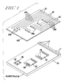
- Figure 1 shows an exploded view of a multichip circuit with overlay layer 20 configured so as to test .
- chips 15 are affixed to substrate 10, as by bonding in place by conventional means using epoxy bonding, thermoplastic bonding, or eutectic die bonding.
- Polymer overlay layer 20 is applied by the following method. Two coats of a solution of methylmethacrylate in THF (tetrahydrofuran) are sprayed over chips 15 with interconnect pads 16. Each coat is dried at a temperature of approximately 150°C for a period of about 5 minutes. A sheet of acetate film 2.54 x 10 ⁇ 2 mm (1 mil) in thickness is laminated to the top of the chips and to package pins 11.
- THF tetrahydrofuran
- a vacuum pressure laminator is preferably employed. Details of a vacuum pressure laminator can be found in application WO88/02551 (RD17433) above.
- Preferable lamination conditions comprise a pressure of approximately 2.11kg/m2 (30 pounds per square inch) at a temperature of about 120°C for a period of about 3 minutes.
- the substrate is then cooled to 80°C and removed from the laminator.
- Via holes over the appropriate chip pads and package pinout pads are fabricated using a focused laser according to the method outlined in application No. WO88/02550 (RD-17,428). Plasma etching is accomplished using somewhat less stringent conditions than required for high stability polymers.
- Metallization is preferably provided by sputtering a 10 ⁇ 4mm (1,000 angstrom) thick layer of titanium, followed by a layer of 10 ⁇ 6m (1 micron) thick copper.
- the metallization is preferably patterned by spraying or spinning a coating of photoresist on the copper surface, drying for about one half hour at approximately 90°C and exposing the positive resist material with a scanned ultraviolet laser under control of computerized artwork.
- a preferable-photoresist material includes Dynachem OFPR 800 photoresist.
- All testing is conducted by applying signals to inputs through the package pins and observing the resultant outputs at the package pins, at least in the embodiment illustrated in Figure 1. It is noted that via holes 26 are aligned with pads 16 on chips 15. It is also noted that vias 21 are aligned with package pins 11. It is further noted that metallization patterns 22 generally extend from via openings 21 to via openings 26 at least for the sample test configuration shown. This pattern may, however, vary over a wide range of patterns.
- FIG. 2 illustrates an alternate embodiment of the present invention in which a test chip 14 is used.
- Test chip 14 is connected to metallization patterns on overlay layer 20′ by means of via openings 24. It is seen in Figure 2 that overlay layer 20′ now makes connections between chip pads 16 and test chip 14. It is noted that more than one test chip may be employed even though the figure illustrates only a single one being used. In the example illustrated in Figure 2, only two connections 23 are shown as being required between the test chip and the package pins. It can be seen through the use of the test chip that packaging pins can be conserved.
- Figure 1 or 2 may then be employed to test the chips 15. Following the testing, overlay layers 20 or 20′ may be removed. Defective chips may be removed or reconfigured or repositioned on the basis of test results obtained. Subsequently, an operational circuit overlay layer 20′′ may be applied to the chip configuration. As a result, the system illustrated in Figure 3 may be produced. It is noted that a difference between Figure 1 and Figure 3 is the particular metallization pattern employed; other differences are discussed hereinafter.
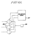
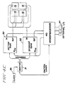
- FIGS 4A, 4B and 4C show three alternative implementations of test chips. In all cases, these configurations use of circuits and technologies well known to those skilled in the art.
- Figure 4A illustrates an array of three transmission gates 38 (typically in CMOS technology). One of the three transmission gates can be selected by selection logic
- the data selector applies the appropriate signal voltages to transmission gases 38 to turn one of the three gates on and to connect external pad 34 to one of three or more possible internal connection points. It is clear that a number of internal connection points can be multiplexed to one outside pin by this method.
- the very high density interconnect capability afforded by the overlay layer allows this method to act as a multiprobe connection system.
- FIG. 4B illustrates an alternate embodiment of the present invention in which memory means 32, such as a random access memory, is employed as a vector generator to supply test vectors to the inputs of a chip or group of chips 15 under test.
- the output of the chip or group of chips is stored in second memory means 33 also typically comprising a random access memory.
- Counter 31 driven by clock 30 provides sequential addresses to sequence the output of test vectors and the storage of test results.
- This system can be run at very high speed, limited only by the speed of the memory means selected.
- the test vectors are supplied at a much more leisurely pace through external input pins 35. Inspection of the results is achieved in a much more leisurely pace by supplying the contents of memory means 33 to external pins 34.
- lines having a hash mark (/) denote multiple signal and/or control paths.
- Figure 4C shows a completely internal configuration for high speed testing.
- microprocessor 40 computes test vectors and supplies them to vector generation random access memory 32.
- the memory is sequentially accessed by the associated counter and the output memory supplies the inputs to a chip or a group of chips 15 under test.
- the resultant outputs from the test are stored in second memory means 33.
- microprocessor 40 reads the test results and compares them to computed results to determine if errors have occurred.
- the entire system can be tested over a long period of time under temperature and variations of other environmental conditions such as electromagnetic interference without any connection, other than power supply, to the outside world.
- Microprocessors can be used to store test results inconsistent with the expected results, thereby identifying the specific chip or chip group and the failure which occurred, even when the failure occurs on an intermittent basis.
- Microprocessor 40 is accessed via external pins 41.
- the test layer is removed according to the following method.
- copper metallization is dissolved in a solution preferably com prising 600 grams of nitric acid, 600 grams sulfuric acid and 600 grams of H3P04 in 1.5 liters of water for a period of about 1 minute. This removes copper, but does not attack either aluminum metallization typically present on the chip pads or titanium which is also preferably (though optionally) present as a barrier layer. Titanium is preferably removed by placement in a solution of fluoroboric acid for a period of about 15 seconds.
- the overlay polymer and adhesive can be removed in a solution of THF for a period of 2 minutes followed by immersion in another clean solution of THF for 1 minute.
- test layer process as described above can be started immediately after a defective chip has been removed and a new one put in place.
- a plasma etch to remove any residual polymer is also preferred.
- Etch conditions preferably include an atmosphere comprising 50% oxygen and 50% CF4 at a total pressure of 53.32N/m2 (0.4 torr) for a period of about 21 ⁇ 2 minutes in an IPC 2000 barrel etcher at a power level of approximately 300 watts.
- the final layer is then provided according to the process described in application No. WO88/02551 (RD-17,433).
- Figure 3 illustrates an exploded view of tested chips on a substrate with an interconnection pattern for an operational circuit.
- the materials used for the final operational configuration preferably involve materials of long term thermal and hydrolitic stability such as KAPTONTM (supplied by Dupont de Nemours Company, Inc.) polyimide film.
- the metallization used preferably comprises slightly thicker material to obviate any problems associated with electromigration or losses due to resistive paths.
- FIG. 5 An alternate approach involving the use of an overlay test layer is shown in an exploded view in Figure 5. This is the same circuit as shown in Figure 3 except that additional overlay layer 60 has been added to provide connections to the test chip or chips, and to the test pins or the package. Also note that operational circuit overlay layer 50 is similar to overlay layer 20′′ illustrated in Figure 3 except for the presence of apertures 24 for connection to test chip 14.
- Test layer 60 can be added by spraying a solution of methylmethacrylate in THF and drying at a temperature of approximately 150°C for a period of 5 minutes. Two such coats are generally required. At this point, via holes are fabricated to the connection points on the layer below by using focused laser energy as described in above-mentioned application No. WO88/02550 (RD-17,428).
- Etch time in an oxygen plasma to clean out the apertures is relatively short since the layer is thin and since the material is highly susceptible to etching.
- Etch conditions 200 watts for 4 minutes in an atmosphere comprising 30% CF4 and 70% oxygen at a pressure of 53.32N/m2 (0.4 Torr) is sufficient.
- Metallization is preferably added by sputtering a layer of chrome which is approximately 10 ⁇ 4mm (1,000 angstroms) thick, followed by sputtering of sufficient copper for conductivity, typically 10 ⁇ 6m (1 micron) in thickness.
- Metallization is patterned, as described above, by a photolithographic method using an etchant of nitric acid, sulfuric acid and H3P04 in water, as above.
- This etchant etches the copper but not the chrome.
- Chrome is etched in a ceric sulfate solution operated at 60°C.
- the test layer is easily removed by dissolving the copper in a copper etch solution. This etch attacks the copper, but does not attack the chrome layer. In this way, the underlying chrome layer protects the copper conductor of the underlying layer where it would be exposed at the interconnect points.
- the chrome is removed with a 25 second etch in the ceric sulfate sulfate solution.
- the test layer polymer dielectric can be removed in a solution of THF, followed by a second immersion in clean THF to remove any residue.
- the underlying KAPTONTM film of the operational interconnect overlay is totally unaffected by the THF solvent.
- the substrate 10 may be of material selected from the group consisting of glass, metal, ceramic, plastic, silicon and composites.
- the polymer film 20′ for testing may be of material selected from the group consisting of thermoplastic materials and thermoset materials.
- the high density interconnect system uses a removable overlay layer to provide a method for directly connecting a large number of chips within the same package.
- the methods disclosed herein provide for the complete test and burn-in of the chip as well as a practical method for partitioning the system into manageable blocks which are easily tested.
- a removable overlay layer can be used to provide a multiplicity of connections throughout the rest of the system for the purpose of system testing and debugging during and after burn-in.
- This approach provides the rough equivalence of a "bed of nails" test fixture which is typically used for printed circuit boards but on a pitch of 2.54 x 10 ⁇ 2mm (1 mil) rather than a pitch of 127 x 10 ⁇ 2mm (50 mils).
- the method and packages disclosed hereinabove provide various ones of the following objectives: a method for testing unpackaged interconnected circuits so as to cause minimum capacitive loading on the chips under test so as to thereby allow tests to be conducted at maximum speed; a method for testing which allows chips to operate in their final locations, such that temperature and environmental conditions (such as electromagnetic interference, radio frequency interference and power supply variations) are all substantially identical to the final desired configuration; a method for testing which allows long term burn-in of chips without tying up expensive test equipment; a method for testing which allows the utilization of special chips, thereby eliminating the need for expensive high speed test equipment, allowing the combination of a multiplicity of chips to be tested at once and reducing the number of external connections or package pins required; a method in which chips can be tested completely with a pad count which exceeds the capability of probe testing with pad sizes which are below the capacity of probe testing; functional testing of multiply interconnected chips which may be done off-line; multiple testing configurations by completely changing the interconnect wiring for one or more chips in the system;
Landscapes
- Engineering & Computer Science (AREA)
- Physics & Mathematics (AREA)
- General Physics & Mathematics (AREA)
- Computer Networks & Wireless Communication (AREA)
- General Engineering & Computer Science (AREA)
- Testing Or Measuring Of Semiconductors Or The Like (AREA)
Abstract
Claims (29)
un substrat (10) ;
un multitude de puces (15) de circuits intégrés disposées sur ledit substrat (10), lesdites puces (15) de circuits intégrés ayant sur leur dessus des plots d'interconnexion (16) ;
un recouvrement amovible par films de polymère (60, 20′) disposé sur les puces et le substrat, ce film ayant des ouvertures (26) qui exposent au moins une partie des plots d'interconnexion ; et
un motif de métallisation disposé sur le film et connectant des plots sélectionnés parmi les plots d'interconnexion par l'intermédiaire desdites ouvertures ;
au moins l'une des puces comprenant une puce de test pouvant fonctionner pour essayer au moins l'une des autres puces.
disposer une multitude de puces (15) à circuits intégrés sur un substrat (10), les puces ayant sur leur dessus des plots d'interconnexion (16) ;
disposer une couche amovible de recouvrement en polymère (20) sur les puces, cette couche (20) comportant au moins des ouvertures (26) en alignement avec au moins certains des plots d'interconnexion (16), la couche ayant également sur son dessus un motif de métallisation (22) pour connecter les puces dans une première configuration;
essayer les puces (15) à circuits intégrés alors qu'elles sont connectées dans la première configuration;
enlever la couche amovible de recouvrement (20') et la métallisation; et
appliquer une seconde couche de recouvrement en polymère (20˝) sur les puces et le substrat, cette seconde couche de recouvrement présentant au moins des ouvertures (26) en alignement avec au moins certains des plots d'interconnexion (16), la seconde couche de recouvrement ayant aussi un motif de métallisation pour connecter les puces (15) dans une seconde configuration.
Applications Claiming Priority (2)
| Application Number | Priority Date | Filing Date | Title |
|---|---|---|---|
| US91245486A | 1986-09-26 | 1986-09-26 | |
| US912454 | 1997-08-18 |
Publications (2)
| Publication Number | Publication Date |
|---|---|
| EP0286660A1 EP0286660A1 (fr) | 1988-10-19 |
| EP0286660B1 true EP0286660B1 (fr) | 1992-03-04 |
Family
ID=25431950
Family Applications (1)
| Application Number | Title | Priority Date | Filing Date |
|---|---|---|---|
| EP87906629A Expired - Lifetime EP0286660B1 (fr) | 1986-09-26 | 1987-09-28 | Procede et configuration de controle de circuits electroniques et de plaquettes de circuits imprimes a l'aide d'une couche amovible de recouvrement |
Country Status (5)
| Country | Link |
|---|---|
| EP (1) | EP0286660B1 (fr) |
| JP (1) | JPH01501031A (fr) |
| KR (1) | KR880701967A (fr) |
| DE (1) | DE3777164D1 (fr) |
| WO (1) | WO1988002549A1 (fr) |
Families Citing this family (12)
| Publication number | Priority date | Publication date | Assignee | Title |
|---|---|---|---|---|
| DE69219165T2 (de) * | 1991-01-11 | 1997-08-07 | Texas Instruments Inc | Prüf- und Einbrennsystem für einen Wafer und Methode für deren Herstellung |
| US5315241A (en) * | 1991-09-18 | 1994-05-24 | Sgs-Thomson Microelectronics, Inc. | Method for testing integrated circuits |
| FR2700063B1 (fr) * | 1992-12-31 | 1995-02-10 | Sgs Thomson Microelectronics | Procédé de test de puces de circuit intégré et dispositif intégré correspondant. |
| EP0662709B1 (fr) * | 1994-01-11 | 1998-03-25 | Siemens Aktiengesellschaft | Méthode de test de couches de circuit semi-conducteur |
| JP2929948B2 (ja) * | 1994-09-20 | 1999-08-03 | 三菱電機株式会社 | プローブ式テストハンドラー及びそれを用いたicのテスト方法 |
| US6468638B2 (en) * | 1999-03-16 | 2002-10-22 | Alien Technology Corporation | Web process interconnect in electronic assemblies |
| US6606247B2 (en) | 2001-05-31 | 2003-08-12 | Alien Technology Corporation | Multi-feature-size electronic structures |
| US7214569B2 (en) | 2002-01-23 | 2007-05-08 | Alien Technology Corporation | Apparatus incorporating small-feature-size and large-feature-size components and method for making same |
| US7253735B2 (en) | 2003-03-24 | 2007-08-07 | Alien Technology Corporation | RFID tags and processes for producing RFID tags |
| DE102004025684B4 (de) | 2004-04-29 | 2024-08-22 | OSRAM Opto Semiconductors Gesellschaft mit beschränkter Haftung | Verfahren zum Ausbilden einer Kontaktstruktur zur elektrischen Kontaktierung eines optoelektronischen Halbleiterchips |
| US7688206B2 (en) | 2004-11-22 | 2010-03-30 | Alien Technology Corporation | Radio frequency identification (RFID) tag for an item having a conductive layer included or attached |
| CN114509659A (zh) * | 2020-11-16 | 2022-05-17 | 中车时代电动汽车股份有限公司 | 电路板测试方法及装置 |
Family Cites Families (3)
| Publication number | Priority date | Publication date | Assignee | Title |
|---|---|---|---|---|
| US4479088A (en) * | 1981-01-16 | 1984-10-23 | Burroughs Corporation | Wafer including test lead connected to ground for testing networks thereon |
| US4426773A (en) * | 1981-05-15 | 1984-01-24 | General Electric Ceramics, Inc. | Array of electronic packaging substrates |
| JPS61111561A (ja) * | 1984-10-05 | 1986-05-29 | Fujitsu Ltd | 半導体装置 |
-
1987
- 1987-09-28 EP EP87906629A patent/EP0286660B1/fr not_active Expired - Lifetime
- 1987-09-28 WO PCT/US1987/002473 patent/WO1988002549A1/fr not_active Ceased
- 1987-09-28 DE DE8787906629T patent/DE3777164D1/de not_active Expired - Lifetime
- 1987-09-28 JP JP62506030A patent/JPH01501031A/ja active Pending
-
1988
- 1988-05-26 KR KR1019880700586A patent/KR880701967A/ko not_active Withdrawn
Non-Patent Citations (2)
| Title |
|---|
| IBM Technical Disclosure Bulletin, volume 24, no. 2, July 1981 (New York, US), L.V. Auletta et al.: "Flexible tape conductor interconnection for chips", pages 1214-1215 * |
| Solid State Technology, volume 29, no. 3, March 1986, (Port Washington, New York, US), W. Lukaszek et al.: "CMOS test chip design for process problem debugging and yield prediction experiments", pages 87-93 * |
Also Published As
| Publication number | Publication date |
|---|---|
| EP0286660A1 (fr) | 1988-10-19 |
| DE3777164D1 (de) | 1992-04-09 |
| KR880701967A (ko) | 1988-11-07 |
| WO1988002549A1 (fr) | 1988-04-07 |
| JPH01501031A (ja) | 1989-04-06 |
Similar Documents
| Publication | Publication Date | Title |
|---|---|---|
| US4937203A (en) | Method and configuration for testing electronic circuits and integrated circuit chips using a removable overlay layer | |
| US4884122A (en) | Method and configuration for testing electronic circuits and integrated circuit chips using a removable overlay layer | |
| US5366906A (en) | Wafer level integration and testing | |
| US5942911A (en) | Electric field test of integrated circuit component | |
| US5897728A (en) | Integrated circuit test structure and test process | |
| US5461328A (en) | Fixture for burn-in testing of semiconductor wafers | |
| US5091769A (en) | Configuration for testing and burn-in of integrated circuit chips | |
| US5149662A (en) | Methods for testing and burn-in of integrated circuit chips | |
| EP0460822B1 (fr) | Unité de circuit intégré utilisant un substrat flexible | |
| US5489538A (en) | Method of die burn-in | |
| US5841193A (en) | Single chip modules, repairable multichip modules, and methods of fabrication thereof | |
| US5576630A (en) | Probe structure for measuring electric characteristics of a semiconductor element | |
| US6262579B1 (en) | Method and structure for detecting open vias in high density interconnect substrates | |
| EP0178227B1 (fr) | Dispositif semiconducteur à circuit intégré formé sur une tranche | |
| JPH07115113A (ja) | 半導体ウエハの試験装置および試験方法 | |
| JPS58207650A (ja) | Icパツケージ | |
| WO1988002549A1 (fr) | Procede et configuration de controle de circuits electroniques et de plaquettes de circuits imprimes a l'aide d'une couche amovible de recouvrement | |
| US3795973A (en) | Multi-level large scale integrated circuit array having standard test points | |
| KR100313185B1 (ko) | 집적 회로 소자의 전기적 액세스 및 상호 접속 방법과 그 장치 | |
| Fillion et al. | Bare chip test techniques for multichip modules | |
| JP3141812B2 (ja) | 回路素子用検査装置 | |
| JPH02156547A (ja) | フレキシブル基板と集積回路のテスト方法 | |
| JP3135135B2 (ja) | 半導体装置,その製造方法,その試験方法及びその試験装置 | |
| US20050104608A1 (en) | Method and system of testing complex MCM's | |
| KR100470123B1 (ko) | 번인 테스트용 보드 및 그 제조 방법과 이를 이용한반도체 칩 번인 테스트 방법 |
Legal Events
| Date | Code | Title | Description |
|---|---|---|---|
| PUAI | Public reference made under article 153(3) epc to a published international application that has entered the european phase |
Free format text: ORIGINAL CODE: 0009012 |
|
| AK | Designated contracting states |
Kind code of ref document: A1 Designated state(s): DE FR GB IT NL SE |
|
| 17P | Request for examination filed |
Effective date: 19880919 |
|
| 17Q | First examination report despatched |
Effective date: 19900307 |
|
| GRAA | (expected) grant |
Free format text: ORIGINAL CODE: 0009210 |
|
| AK | Designated contracting states |
Kind code of ref document: B1 Designated state(s): DE FR GB IT NL SE |
|
| PG25 | Lapsed in a contracting state [announced via postgrant information from national office to epo] |
Ref country code: IT Free format text: LAPSE BECAUSE OF FAILURE TO SUBMIT A TRANSLATION OF THE DESCRIPTION OR TO PAY THE FEE WITHIN THE PRE;WARNING: LAPSES OF ITALIAN PATENTS WITH EFFECTIVE DATE BEFORE 2007 MAY HAVE OCCURRED AT ANY TIME BEFORE 2007. THE CORRECT EFFECTIVE DATE MAY BE DIFFERENT FROM THE ONE RECORDED.SCRIBED TIME-LIMIT Effective date: 19920304 Ref country code: SE Effective date: 19920304 Ref country code: FR Effective date: 19920304 Ref country code: NL Effective date: 19920304 |
|
| REF | Corresponds to: |
Ref document number: 3777164 Country of ref document: DE Date of ref document: 19920409 |
|
| EN | Fr: translation not filed | ||
| NLV1 | Nl: lapsed or annulled due to failure to fulfill the requirements of art. 29p and 29m of the patents act | ||
| PG25 | Lapsed in a contracting state [announced via postgrant information from national office to epo] |
Ref country code: GB Effective date: 19920928 |
|
| PLBE | No opposition filed within time limit |
Free format text: ORIGINAL CODE: 0009261 |
|
| STAA | Information on the status of an ep patent application or granted ep patent |
Free format text: STATUS: NO OPPOSITION FILED WITHIN TIME LIMIT |
|
| 26N | No opposition filed | ||
| GBPC | Gb: european patent ceased through non-payment of renewal fee |
Effective date: 19920928 |
|
| PG25 | Lapsed in a contracting state [announced via postgrant information from national office to epo] |
Ref country code: DE Effective date: 19930602 |
|
| EUG | Se: european patent has lapsed |
Ref document number: 87906629.8 Effective date: 19920214 |