EP0286917A2 - Cellule solaire - Google Patents
Cellule solaire Download PDFInfo
- Publication number
- EP0286917A2 EP0286917A2 EP88105201A EP88105201A EP0286917A2 EP 0286917 A2 EP0286917 A2 EP 0286917A2 EP 88105201 A EP88105201 A EP 88105201A EP 88105201 A EP88105201 A EP 88105201A EP 0286917 A2 EP0286917 A2 EP 0286917A2
- Authority
- EP
- European Patent Office
- Prior art keywords
- solar cell
- semiconductor substrate
- ohmic contacts
- silicon
- charge carriers
- Prior art date
- Legal status (The legal status is an assumption and is not a legal conclusion. Google has not performed a legal analysis and makes no representation as to the accuracy of the status listed.)
- Granted
Links
Images


Classifications
-
- H—ELECTRICITY
- H10—SEMICONDUCTOR DEVICES; ELECTRIC SOLID-STATE DEVICES NOT OTHERWISE PROVIDED FOR
- H10F—INORGANIC SEMICONDUCTOR DEVICES SENSITIVE TO INFRARED RADIATION, LIGHT, ELECTROMAGNETIC RADIATION OF SHORTER WAVELENGTH OR CORPUSCULAR RADIATION
- H10F77/00—Constructional details of devices covered by this subclass
- H10F77/10—Semiconductor bodies
- H10F77/14—Shape of semiconductor bodies; Shapes, relative sizes or dispositions of semiconductor regions within semiconductor bodies
- H10F77/147—Shapes of bodies
-
- H—ELECTRICITY
- H10—SEMICONDUCTOR DEVICES; ELECTRIC SOLID-STATE DEVICES NOT OTHERWISE PROVIDED FOR
- H10F—INORGANIC SEMICONDUCTOR DEVICES SENSITIVE TO INFRARED RADIATION, LIGHT, ELECTROMAGNETIC RADIATION OF SHORTER WAVELENGTH OR CORPUSCULAR RADIATION
- H10F10/00—Individual photovoltaic cells, e.g. solar cells
- H10F10/10—Individual photovoltaic cells, e.g. solar cells having potential barriers
- H10F10/12—Photovoltaic cells having only metal-insulator-semiconductor [MIS] potential barriers
-
- H—ELECTRICITY
- H10—SEMICONDUCTOR DEVICES; ELECTRIC SOLID-STATE DEVICES NOT OTHERWISE PROVIDED FOR
- H10F—INORGANIC SEMICONDUCTOR DEVICES SENSITIVE TO INFRARED RADIATION, LIGHT, ELECTROMAGNETIC RADIATION OF SHORTER WAVELENGTH OR CORPUSCULAR RADIATION
- H10F77/00—Constructional details of devices covered by this subclass
- H10F77/20—Electrodes
- H10F77/206—Electrodes for devices having potential barriers
- H10F77/211—Electrodes for devices having potential barriers for photovoltaic cells
- H10F77/215—Geometries of grid contacts
-
- H—ELECTRICITY
- H10—SEMICONDUCTOR DEVICES; ELECTRIC SOLID-STATE DEVICES NOT OTHERWISE PROVIDED FOR
- H10F—INORGANIC SEMICONDUCTOR DEVICES SENSITIVE TO INFRARED RADIATION, LIGHT, ELECTROMAGNETIC RADIATION OF SHORTER WAVELENGTH OR CORPUSCULAR RADIATION
- H10F77/00—Constructional details of devices covered by this subclass
- H10F77/30—Coatings
- H10F77/306—Coatings for devices having potential barriers
- H10F77/311—Coatings for devices having potential barriers for photovoltaic cells
-
- Y—GENERAL TAGGING OF NEW TECHNOLOGICAL DEVELOPMENTS; GENERAL TAGGING OF CROSS-SECTIONAL TECHNOLOGIES SPANNING OVER SEVERAL SECTIONS OF THE IPC; TECHNICAL SUBJECTS COVERED BY FORMER USPC CROSS-REFERENCE ART COLLECTIONS [XRACs] AND DIGESTS
- Y02—TECHNOLOGIES OR APPLICATIONS FOR MITIGATION OR ADAPTATION AGAINST CLIMATE CHANGE
- Y02E—REDUCTION OF GREENHOUSE GAS [GHG] EMISSIONS, RELATED TO ENERGY GENERATION, TRANSMISSION OR DISTRIBUTION
- Y02E10/00—Energy generation through renewable energy sources
- Y02E10/50—Photovoltaic [PV] energy
- Y02E10/547—Monocrystalline silicon PV cells
Definitions
- the invention relates to a solar cell, in particular thin-film solar cell made of a semiconductor material such as silicon, in the semiconductor substrate of which minority and majority charge carriers are generated by radiation energy, which are separable by an electric field and then derivable, with a (first) semiconductor substrate surface mutually spaced ohmic contacts are arranged, which are interconnected, and at least between the ohmic contacts a passivation layer is arranged, which preferably also covers the ohmic contacts. Furthermore, the invention also relates to a method for producing a solar cell.
- the recombination of charge carriers in the region of the ohmic contacts can be reduced without a potential threshold for minority charge carriers having to be generated in the semiconductor substrate by alloying, diffusion or ion implantation.
- the object of the present invention is therefore to design a solar cell of the type described in the introduction in such a way that the thickness of the semiconductor substrate can be reduced considerably without that the risk of increased recombination in the area of ohmic contacts increases. Rather, despite the reduction in the semiconductor material thickness, the recombination in the area of the ohmic contacts is to be reduced further, the charge carriers not necessarily having to be kept away from the ohmic contacts by a potential barrier.
- the object is achieved in that the electric field separating the minority and majority charge carriers extends in the region of a (second) substrate body surface which is opposite the first substrate body surface having the ohmic contact regions, so that the majority charge carriers diffuse to the ohmic contact regions and of these are collected and that the ohmic contacts are arranged on first regions of the first semiconductor substrate surface which are raised opposite second regions of the semiconductor substrate which are present between the ohmic contacts.
- the ohmic contacts serve to collect the majority charge carriers and are attached directly to the substrate material without a doped intermediate layer (ie without special shielding by means of a potential barrier). Due to the lack of the potential barrier, in addition to the majority charge carriers, minority charge carriers could in principle also reach the ohmic contacts, even if the latter should diffuse with ideal behavior to the separating electrical field on the side opposite the ohmic contacts. However, in order to reduce a recombination of majority and minority charge carriers in the area of the ohmic contacts, it is proposed according to the invention that the ohmic contacts are applied, for example as narrow strips, in an elevated manner compared to their surroundings, which are very well passivated with an insulator layer.
- the ohmic contacts according to the prior art do not have the task of improving the stability of thin-film solar cells, that is to say cells which have a substrate thickness which is so thin that there is a risk of breakage.
- the ohmic contacts are spatially separated from the other semiconductor surface, which is very well passivated by the passivation layer (insulator layer).
- the passivation layer insulator layer.
- a semiconductor substrate thickness that is smaller than the diffusion length of the minority charge carriers can be selected outside the ohmic contacts, so that a high efficiency of the solar cell can be achieved.
- the recombination is not increased in the area of the ohmic contacts, since in this area the distance to the opposite side of the semiconductor substrate is preferably considerably greater than the diffusion length of the minority charge carriers.
- the semiconductor surface having the ohmic contacts is preferably structured by selective etching. This is based on a correspondingly thick semiconductor wafer, which is preferably stronger than the diffusion length of the minority charge carriers.
- the ohmic contact areas are then determined in order to cover them with a suitable etching mask.
- the uncovered areas are then etched away to the desired thickness of the semiconductor substrate. If the etching mask is not simultaneously formed by the metal of the ohmic contacts — a further feature according to the invention can be seen here — the etching mask is removed after the etching in order to apply the metal of the ohmic contact if necessary.
- an etching mask e.g. Photoresist, SiO2 or Si3N4 can be used. There is also the possibility that the metal is under the etching mask.
- the etching itself can be isotropic or anisotropic, chemical etching or plasma, ion, reactive ion or laser etching.
- anisotropic etching is particularly advantageous when using (100) oriented silicon, since it is known that the (100) surface is etched much faster than the (111) surface. In this case, there are trapezoidal sections under the etching mask, the edge angle of which is 54.7 °. The ohmic contacts are then applied to the tips, that is to say the outer end faces of these regions.
- the known structure etches based on, for example, potassium hydroxide or ethylenediamine are particularly suitable as anisotropic etchants.
- Surfaces can also advantageously be used in connection with the anisotropic etching, with raised areas delimited by vertical walls. The cut is rectangular.
- the ohmic contacts also serve as an etching mask. Together with the etching process, the uncovered areas are textured at the same time in order to increase the incidence of light of the Si surface passivated with the insulator layer.
- these e.g. can be applied by vacuum evaporation through a mechanical mask, by screen printing, by sputtering and, if necessary, structured with photolithography.
- the raised areas intended for the ohmic contacts also have the advantage that the semiconductor substrate becomes more stable, even if the layer thickness between the elevations is extremely small, without the risk of susceptibility to breakage. This is particularly important when using cheaper single-crystal and polycrystalline ("solar-grade”) silicon material, which has a shorter diffusion length for the minority charge carriers.
- Another advantage of the design of the solar cell according to the invention is that the contacting of thin solar cells is made considerably easier, for example by ultrasonic welding, in that this is done on the thick semiconductor region covered by the ohmic contacts or on an additional but simultaneously with the etching of the ohms 'Contact areas generated at the edge made of thick semiconductor material without risk of breaking the thin silicon areas. Furthermore, this arrangement with a passivation layer extending over the edge of the solar cell allows the front-side contact to pass over the edge led to the back and contacted there. Contacting both connections on one side - e.g. using ultrasound - significantly simplifies the manufacturing process.
- the structure of the solar cell proposed according to the invention can be used for single and polycrystalline silicon and for compound semiconductors.
- Embodiments of the invention result from the claims and the features to be extracted from them - individually and / or in combination.
- FIG. 1 shows the embodiment of a solar cell (19) constructed according to the invention, which consists of a p-doped silicon substrate as the body (1), a thin silicon oxide layer (2), ohmic contacts (4) and an MIS (metal) Insulator semiconductor) contact, which in turn consists of the p-silicon of the silicon body (1), the silicon oxide layer (2) and a metallization (3) preferably made of aluminum or magnesium or a double layer of Mg / Al put together.
- the ohmic contacts (4) are arranged discontinuously on the semiconductor substrate (1), these being arranged according to the invention on the free end faces (31) of elevations (21).
- the ohmic contacts (4), together with the elevated silicon regions (21) underneath, can form a geometry that can be described by interconnected strips, rings or dots.
- Passivation layers extend between the elevated ohmic contact areas (4), which are composed on the one hand of the natural or below 800 ° C silicon oxide layer (2) and a further insulator layer (5), both for passivation and as an anti-reflection layer can serve.
- the thickness of the upper passivation layer (5), referred to as the first, can be approximately 80 nm and preferably consists of aluminum oxide or silicon nitride.
- the further insulator layer, which is referred to as the second passivation layer, in the form of the silicon oxide layer (2) can be constructed differently on the front and back of the silicon substrate (1). The thickness on the front can be varied within wide limits since it does not act as a tunnel insulator. However, it can also be completely omitted there.
- a natural silicon oxide layer is understood to be that which is always present on the silicon substrate (1) and is only a few atomic layers thick.
- the structure of the silicon oxide layer (2) itself can be changed on the front side by the subsequent deposition of the first passivation layer (5), for example silicon nitride.
- silicon oxide can be converted into silicon oxynitride.
- the charge carriers generated mainly by the light near the front first have to diffuse through the entire substrate (1) in order to be collected by the MIS contact on the back. It is extremely important that the front side, which is composed of the area of the ohmic contacts (4) and the silicon surface covered by the passivation layers (2) and (5), has a low surface recombination speed, since otherwise a large part of the Charge carriers would already recombine there.
- the ohmic contacts (4) are lifted out of the surface by a silicon etching process and, depending on the height of the regions, their influence on recombination is more or less eliminated.
- This measure namely increases the distance between the ohmic contacts (4) both from the point of generation of the charge carriers in the silicon volume (1) and from the collecting MIS contact (3), so that the minority charge carriers prefer to the MIS because of the now higher concentration gradient - Diffuse contact and be used there.
- the distance between the ohmic contacts (4) (surface (31)) and the opposite MIS contact (3) (surface (27)) should advantageously be greater than the diffusion length of the minority charge carriers.
- the thickness of the silicon substrate (1) in the region (22) can be greater, equal or smaller, but preferably considerably smaller than the diffusion length. If, however, the thickness is considerably smaller than the diffusion length, as many of the minority charge carriers that are formed on the surface can diffuse to the rear, without recombining.
- This optimization of the substrate thickness and the height of the ohmic contact areas can take place independently of one another by means of the arrangement according to the invention, by suitable choice of the starting layer thickness of the silicon and by the duration of the etching process.
- Another advantage is that the raised silicon webs (21) under the ohmic contact (4) serve as mechanical reinforcement for the silicon volume (1).
- the ohmic contacts (4) are preferably arranged in the shape of a finger, i. that is, they are composed of webs that run parallel to one another and are connected to one another on one side (comb shape).
- the distance between the ohmic contact fingers should be much greater than the thickness d (distance between surfaces (22) and (27)) of the silicon substrate (1) or as the diffusion length of the minority charge carriers, so that on average the way to collect them MIS contact is less than to the ohmic contact area.
- the distance between the ohmic contacts (4) is limited by the series resistance.
- the optimal distance is in the range of 1 to 5 mm, the finger width in the range of 50 to 300 ⁇ m, which means that a proportion of contact area or shading of less than 10% can be achieved.
- the rear metal (3) of the MIS contact serves as a reflector for the light not absorbed, so that the light path in the silicon and thus the generation of charge carriers is essential is increased, which in particular enables the advantageous use of very thin, cheap solar silicon.
- the reflection of the infrared portion of the sunlight on the back leads to less heating of the solar cell and thus to a higher efficiency under real operating conditions.
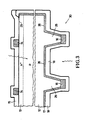
- FIG. 2 and 3 show further configurations of solar cells (20) and (30) which obey the teaching according to the invention.
- the respective ohmic contact (10) or (16) is arranged on the back of the solar cell (20) or (30), specifically directly on the semiconductor substrate body (6) or (21) and also in regions, such as it was already the case in FIG. 1.
- the solar cell (20) shown in FIG. 2 corresponds to the basic structure according to the silicon nitride inversion layer solar cell described in DE-PS 28 40 096 with MIS contacts.
- the solar cell (20) has a p-silicon substrate or body (6) on which a thin silicon oxide layer (7) is arranged.
- MIS contacts are arranged on the front, which are composed of the semiconductor substrate (6), the silicon oxide layer (7) and discontinuously of metal layers (8) which are preferably arranged in strip form.
- the electrons (minority charge carriers) generated by the light diffuse to the front and are accelerated there in the electrical field generated by the positive insulator charges and migrate along the highly conductive inversion layer to the MIS contacts, through which they leave the silicon body (6) and reach an external circuit.
- a further passivation layer (11) is also provided, which also covers the ohmic contacts (10).
- the decisive training is then to be found that the ohmic contacts (10) are raised, i.e. on protrusions (23) which rise from the normal surface (24) and are formed by a silicon etching process.
- the influence of the ohmic contacts (10) on the recombination of the charge carriers is greatly reduced or is completely eliminated at distances from the point of origin which are considerably greater than the diffusion length.
- the actual silicon substrate (6) can thus be made thinner without increasing the recombination. As a result, both the efficiency in terms of the light coming in from the front and the light coming in from the rear is significantly increased.
- the decisive advantage also applies here that the mechanical stability of the thin silicon substrate (6) is significantly improved by the silicon elevations or struts (23) below the ohmic contact (10) and thus the economical production of highly efficient extremely thin (d ⁇ 50 ⁇ m) ) silicon solar cells that can be illuminated on both sides is only possible. It should be noted in particular that this takes place without any significant additional technological effort.
- Silicon nitride or silicon oxynitride (produced in plasma) or aluminum oxide or aluminum oxynitride are preferably suitable for passivating the rear side by means of the transparent passivation or insulator layer (11).
- the production temperatures are between 300 ° C and 600 ° C.
- the function of these layers on the back is completely different from that on the front. In the latter case, high positive charges must be present at the interface so that a highly conductive inversion layer (electron gas) is generated just below the surface.
- the surface recombination speed must be greatly reduced; a highly conductive inversion layer is rather harmful here, since it leads the minority charge carriers to the ohmic contacts, where they recombine and are therefore lost from use.
- the rear silicon nitride layer (11) is produced at higher temperatures compared to the nitride layer (9) on the front.
- the surface recombination is thus reduced. This means that the inversion layer that arises due to the high charge densities or that is greatly increased in its conductivity is accepted.
- the present invention with the ohmic contacts (10) reset by etching also considerably reduces the disadvantageous influence of the inversion layer, in that constant distance between the ohmic contacts, the length of the inversion layer and thus its resistance is considerably increased, and the flow of the minority charge carriers to the ohmic contacts is severely restricted.
- the recombination can be reduced further by means of higher insulator charge densities, without having to accept the additional disadvantage with regard to the inversion layer.
- This advantage also applies to the solar cell shown in FIG. 1 with the raised ohmic contact grid on the front.
- Aluminum oxide as the insulator layer (11) contains negative charges, which lead to an accumulation of holes on the silicon surface on p-silicon.
- the problem with the inversion layer advantageously does not occur there, the electrons as minority charge carriers are repelled by the potential barrier from the rear.
- a highly reflective metal e.g. Al, Ag
- the transparent insulator layer (11) over the entire back, for example by vacuum evaporation or sputtering.
- a highly reflective metal e.g. Al, Ag
- the path of the light incident from the front in the silicon is doubled by reflection and the efficiency is increased, in particular for thin, cheap solar silicon.
- FIG. 3 shows a solar cell (30) which obeys the teaching according to the invention and which can be a conventional n+p or p+n solar cell.
- the n+p solar cell (30) shown in the exemplary embodiment comprises a semiconductor substrate (12), a highly doped surface layer (13) (here n+), on the front side an ohmic contact (14) in the form of a lattice and not arranged flat a front anti-reflective layer (15).
- On the back side there are also ohmic contacts (16) and passivation layers which are arranged in a non-planar manner, preferably in the form of a web or grid, preferably in the form of a silicon oxide layer (17) and an insulating layer (18) which also acts as an antireflection layer.
- the insulating layer (18) is preferably formed from aluminum oxide or silicon nitride.
- the ohmic contacts (16) are now preferably arranged in the form of fingers on elevations (25) which are lifted out of the surface (26) by silicon etching.
- the ohmic contacts (16) are clearly covered by the passivation layer (18).
- the inventive design of the solar cell (30) achieves the same advantages as the solar cell (20) according to FIG. 2.
- a difference between the two cells (20) and (30) lies in the fact that the solar cell (30) with pn- Transition contained high temperature processes, while the entire solar cell (20) is manufactured by simple low temperature processes.
- Both solar cells can take advantage of both the solar radiation hitting the front and the rear.
- a reflective metal can be applied to the back.
Landscapes
- Photovoltaic Devices (AREA)
Applications Claiming Priority (2)
| Application Number | Priority Date | Filing Date | Title |
|---|---|---|---|
| DE19873712503 DE3712503A1 (de) | 1987-04-13 | 1987-04-13 | Solarzelle |
| DE3712503 | 1987-04-13 |
Publications (3)
| Publication Number | Publication Date |
|---|---|
| EP0286917A2 true EP0286917A2 (fr) | 1988-10-19 |
| EP0286917A3 EP0286917A3 (en) | 1990-01-17 |
| EP0286917B1 EP0286917B1 (fr) | 1992-09-02 |
Family
ID=6325536
Family Applications (1)
| Application Number | Title | Priority Date | Filing Date |
|---|---|---|---|
| EP88105201A Expired - Lifetime EP0286917B1 (fr) | 1987-04-13 | 1988-03-30 | Cellule solaire |
Country Status (8)
| Country | Link |
|---|---|
| US (1) | US4886555A (fr) |
| EP (1) | EP0286917B1 (fr) |
| JP (1) | JPS6453468A (fr) |
| CN (1) | CN1011452B (fr) |
| AU (1) | AU600573B2 (fr) |
| DE (2) | DE3712503A1 (fr) |
| ES (1) | ES2033972T3 (fr) |
| IN (1) | IN171031B (fr) |
Cited By (4)
| Publication number | Priority date | Publication date | Assignee | Title |
|---|---|---|---|---|
| WO1992014270A1 (fr) * | 1991-02-04 | 1992-08-20 | Gesellschaft Zur Förderung Der Industrieorientierten Forschung An Den Schweizerischen Hochschulen Und Weiteren Institutionen Eth - Zentrum (Ifw) | Cellule solaire |
| EP0548863A1 (fr) * | 1991-12-27 | 1993-06-30 | Rudolf Dr. Hezel | Procédé pour la fabrication d'une cellule solaire et cellule solaire |
| WO2002061851A1 (fr) | 2001-01-31 | 2002-08-08 | Shin-Etsu Handotai Co.,Ltd. | Cellule solaire et son procede de fabrication |
| CN100437991C (zh) * | 2004-12-08 | 2008-11-26 | 鸿富锦精密工业(深圳)有限公司 | 散热装置及其制备方法 |
Families Citing this family (30)
| Publication number | Priority date | Publication date | Assignee | Title |
|---|---|---|---|---|
| DE3917048A1 (de) * | 1989-05-25 | 1990-11-29 | Damaso Moreno | Folienartiges material fuer eine faltpackung und derartige faltpackung |
| JP3398385B2 (ja) * | 1993-07-29 | 2003-04-21 | ヴィレケ・ゲルハルト | 太陽電池の製作方法およびこの方法によって製作された太陽電池 |
| DE19741832A1 (de) * | 1997-09-23 | 1999-03-25 | Inst Solarenergieforschung | Verfahren zur Herstellung einer Solarzelle und Solarzelle |
| JP3557148B2 (ja) * | 2000-02-21 | 2004-08-25 | 三洋電機株式会社 | 太陽電池モジュール |
| JP4291521B2 (ja) * | 2001-03-23 | 2009-07-08 | 日本オプネクスト株式会社 | 半導体受光素子、半導体受光装置、半導体装置、光モジュール及び光伝送装置 |
| US20070295381A1 (en) * | 2004-03-29 | 2007-12-27 | Kyocera Corporation | Solar Cell Module and Photovoltaic Power Generator Using This |
| US7754964B2 (en) | 2005-08-24 | 2010-07-13 | The Trustees Of Boston College | Apparatus and methods for solar energy conversion using nanocoax structures |
| US7634162B2 (en) | 2005-08-24 | 2009-12-15 | The Trustees Of Boston College | Apparatus and methods for nanolithography using nanoscale optics |
| US7589880B2 (en) | 2005-08-24 | 2009-09-15 | The Trustees Of Boston College | Apparatus and methods for manipulating light using nanoscale cometal structures |
| US7943847B2 (en) | 2005-08-24 | 2011-05-17 | The Trustees Of Boston College | Apparatus and methods for solar energy conversion using nanoscale cometal structures |
| US7649665B2 (en) | 2005-08-24 | 2010-01-19 | The Trustees Of Boston College | Apparatus and methods for optical switching using nanoscale optics |
| US8816191B2 (en) * | 2005-11-29 | 2014-08-26 | Banpil Photonics, Inc. | High efficiency photovoltaic cells and manufacturing thereof |
| EP2319087A1 (fr) | 2008-06-11 | 2011-05-11 | Solar Implant Technologies Inc. | Fabrication de cellule solaire avec facettage et implantation ionique |
| DE102009024807B3 (de) * | 2009-06-02 | 2010-10-07 | Helmholtz-Zentrum Berlin Für Materialien Und Energie Gmbh | Solarzelle mit benachbarten elektrisch isolierenden Passivierbereichen mit hoher Oberflächenladung gegensätzlicher Polarität und Herstellungsverfahren |
| US8749053B2 (en) | 2009-06-23 | 2014-06-10 | Intevac, Inc. | Plasma grid implant system for use in solar cell fabrications |
| EP2290704A1 (fr) * | 2009-08-27 | 2011-03-02 | Applied Materials, Inc. | Couche de passivation pour cellules solaires à base de plaquette en silicon crystallin et son procédé de fabrication |
| DE102009044052A1 (de) * | 2009-09-18 | 2011-03-24 | Schott Solar Ag | Kristalline Solarzelle, Verfahren zur Herstellung einer solchen sowie Verfahren zur Herstellung eines Solarzellenmoduls |
| KR20110049218A (ko) * | 2009-11-04 | 2011-05-12 | 삼성전자주식회사 | 태양 전지 및 그 제조 방법 |
| DE102011051019B4 (de) * | 2011-06-10 | 2021-10-07 | Hanwha Q Cells Gmbh | Solarzellenherstellungsverfahren |
| CN102222706B (zh) * | 2011-06-28 | 2012-11-14 | 厦门市三安光电科技有限公司 | 一种高倍聚光太阳能电池芯片 |
| MY175007A (en) | 2011-11-08 | 2020-06-02 | Intevac Inc | Substrate processing system and method |
| KR101860919B1 (ko) | 2011-12-16 | 2018-06-29 | 엘지전자 주식회사 | 태양 전지 및 이의 제조 방법 |
| US9318332B2 (en) | 2012-12-19 | 2016-04-19 | Intevac, Inc. | Grid for plasma ion implant |
| JP6430090B1 (ja) * | 2017-04-27 | 2018-11-28 | 京セラ株式会社 | 太陽電池素子および太陽電池素子の製造方法 |
| US10971647B2 (en) * | 2018-05-07 | 2021-04-06 | Amberwave, Inc. | Solar cell via thin film solder bond |
| CN113675722B (zh) * | 2021-07-14 | 2024-10-29 | 威科赛乐微电子股份有限公司 | 一种Cap layer层蚀刻优化方法 |
| CN118156325A (zh) | 2022-12-07 | 2024-06-07 | 浙江晶科能源有限公司 | 太阳能电池及光伏组件 |
| CN118156335A (zh) * | 2022-12-07 | 2024-06-07 | 浙江晶科能源有限公司 | 太阳能电池及光伏组件 |
| CN116314382B (zh) | 2023-05-16 | 2023-09-08 | 天合光能股份有限公司 | 太阳能电池及其制作方法、光伏组件及光伏系统 |
| CN117276356A (zh) * | 2023-06-02 | 2023-12-22 | 天合光能股份有限公司 | 太阳能电池及其制作方法、光伏组件及光伏系统 |
Family Cites Families (10)
| Publication number | Priority date | Publication date | Assignee | Title |
|---|---|---|---|---|
| JPS5165774U (fr) * | 1974-11-20 | 1976-05-24 | ||
| US4135950A (en) * | 1975-09-22 | 1979-01-23 | Communications Satellite Corporation | Radiation hardened solar cell |
| US4253881A (en) * | 1978-10-23 | 1981-03-03 | Rudolf Hezel | Solar cells composed of semiconductive materials |
| DE3016498A1 (de) * | 1980-04-29 | 1981-11-05 | Siemens AG, 1000 Berlin und 8000 München | Lichtempfindliche halbleiterbauelemente |
| JPS577168A (en) * | 1980-06-14 | 1982-01-14 | Shunpei Yamazaki | Manufacture of mis photoelectric converter |
| US4322571A (en) * | 1980-07-17 | 1982-03-30 | The Boeing Company | Solar cells and methods for manufacture thereof |
| FR2499316A1 (fr) * | 1981-02-04 | 1982-08-06 | Radiotechnique Compelec | Perfectionnement a la realisation d'une cellule solaire en vue, notamment, de modeler l'epaisseur de sa couche active, et cellule ainsi obtenue |
| US4367368A (en) * | 1981-05-15 | 1983-01-04 | University Patents Inc. | Solar cell |
| FR2556135B1 (fr) * | 1983-12-02 | 1986-09-19 | Thomson Csf | Photo-diode a l'antimoniure d'indium et procede de fabrication |
| DE3536299A1 (de) * | 1985-10-11 | 1987-04-16 | Nukem Gmbh | Solarzelle aus silizium |
-
1987
- 1987-04-13 DE DE19873712503 patent/DE3712503A1/de not_active Withdrawn
-
1988
- 1988-03-30 DE DE8888105201T patent/DE3874184D1/de not_active Expired - Fee Related
- 1988-03-30 ES ES198888105201T patent/ES2033972T3/es not_active Expired - Lifetime
- 1988-03-30 EP EP88105201A patent/EP0286917B1/fr not_active Expired - Lifetime
- 1988-03-31 US US07/176,286 patent/US4886555A/en not_active Expired - Fee Related
- 1988-04-05 IN IN280/CAL/88A patent/IN171031B/en unknown
- 1988-04-12 AU AU14522/88A patent/AU600573B2/en not_active Ceased
- 1988-04-13 CN CN88101994A patent/CN1011452B/zh not_active Expired
- 1988-04-13 JP JP63091234A patent/JPS6453468A/ja active Pending
Cited By (8)
| Publication number | Priority date | Publication date | Assignee | Title |
|---|---|---|---|---|
| WO1992014270A1 (fr) * | 1991-02-04 | 1992-08-20 | Gesellschaft Zur Förderung Der Industrieorientierten Forschung An Den Schweizerischen Hochschulen Und Weiteren Institutionen Eth - Zentrum (Ifw) | Cellule solaire |
| AU652998B2 (en) * | 1991-02-04 | 1994-09-15 | Paul Scherrer Institut | Solar cell |
| EP0548863A1 (fr) * | 1991-12-27 | 1993-06-30 | Rudolf Dr. Hezel | Procédé pour la fabrication d'une cellule solaire et cellule solaire |
| US5356488A (en) * | 1991-12-27 | 1994-10-18 | Rudolf Hezel | Solar cell and method for its manufacture |
| US5449626A (en) * | 1991-12-27 | 1995-09-12 | Hezel; Rudolf | Method for manufacture of a solar cell |
| WO2002061851A1 (fr) | 2001-01-31 | 2002-08-08 | Shin-Etsu Handotai Co.,Ltd. | Cellule solaire et son procede de fabrication |
| EP1365455A4 (fr) * | 2001-01-31 | 2006-09-20 | Shinetsu Handotai Kk | Cellule solaire et son procede de fabrication |
| CN100437991C (zh) * | 2004-12-08 | 2008-11-26 | 鸿富锦精密工业(深圳)有限公司 | 散热装置及其制备方法 |
Also Published As
| Publication number | Publication date |
|---|---|
| JPS6453468A (en) | 1989-03-01 |
| EP0286917A3 (en) | 1990-01-17 |
| DE3712503A1 (de) | 1988-11-03 |
| IN171031B (fr) | 1992-07-04 |
| AU1452288A (en) | 1988-10-13 |
| US4886555A (en) | 1989-12-12 |
| ES2033972T3 (es) | 1993-04-01 |
| DE3874184D1 (de) | 1992-10-08 |
| EP0286917B1 (fr) | 1992-09-02 |
| CN88101994A (zh) | 1988-10-26 |
| CN1011452B (zh) | 1991-01-30 |
| AU600573B2 (en) | 1990-08-16 |
Similar Documents
| Publication | Publication Date | Title |
|---|---|---|
| EP0286917B1 (fr) | Cellule solaire | |
| DE69837143T2 (de) | Ein Verfahren zur Herstellung einer Solarzelle | |
| EP0219763B1 (fr) | Cellule solaire | |
| EP0548863B1 (fr) | Procédé pour la fabrication d'une cellule solaire et cellule solaire | |
| DE102011122252B4 (de) | Solarzelle und Verfahren zu deren Herstellung | |
| DE3446885A1 (de) | Mittels laser gekerbte solarzelle | |
| WO2009074469A2 (fr) | Cellule solaire à contact arrière comportant des zones d'émetteur de côté arrière de grande surface et procédé de fabrication de la cellule solaire | |
| DE4426347A1 (de) | Flaches Bauelement mit einem Gitternetz von Durchgangslöchern | |
| DE19522539A1 (de) | Solarzelle mit einem, eine Oberflächentextur aufweisenden Emitter sowie Verfahren zur Herstellung derselben | |
| DE212023000147U1 (de) | Rückkontaktzelle | |
| DE102012000541A1 (de) | Solarzelle und Verfahren zur Herstellung derselben | |
| WO2006128427A2 (fr) | Procede pour produire une pile solaire a contact unilateral et pile solaire a contact unilateral | |
| DE102011050089A1 (de) | Verfahren zum Herstellen von elektrischen Kontakten an einer Solarzelle, Solarzelle und Verfahren zum Herstellen eines Rückseiten-Kontaktes einer Solarzelle | |
| DE3819671C2 (fr) | ||
| EP2347448B1 (fr) | Procédé pour produire une cellule solaire à hétérojonction sur plaquette à mise en contact sur la face arrière et cellule solaire à hétérojonction produite selon ce procédé | |
| EP2671264B1 (fr) | Cellule solaire photovoltaïque et son procédé de fabrication | |
| EP2107615A2 (fr) | Cellule solaire et procédé de fabrication d'une cellule solaire | |
| EP2135291A2 (fr) | Procédé de fabrication d'une cellule solaire et cellule solaire ainsi fabriquée | |
| DE102011115581B4 (de) | Verfahren zur Herstellung einer Solarzelle | |
| DE112020001695T5 (de) | Solarzellen mit Hybridarchitekturen einschließlich abgegrenzter P- und N-Regionen mit versetzten Kontakten | |
| EP3857617B1 (fr) | Procédé de séparation d'un composant semi-conducteur muni d'une jonction pn | |
| DE102010020557A1 (de) | Verfahren zur Herstellung einer einseitig kontaktierbaren Solarzelle aus einem Silizium-Halbleitersubstrat | |
| WO1998047184A1 (fr) | Procede de fabrication d'un systeme de cellules photovoltaiques individuelles disposees en serie, et le systeme en question | |
| DE102009024598A1 (de) | Solarzelle mit Kontaktstruktur mit geringen Rekombinationsverlusten sowie Herstellungsverfahren für solche Solarzellen | |
| DE4143084A1 (de) | Verfahren zur herstellung einer solarzelle sowie solarzelle |
Legal Events
| Date | Code | Title | Description |
|---|---|---|---|
| PUAI | Public reference made under article 153(3) epc to a published international application that has entered the european phase |
Free format text: ORIGINAL CODE: 0009012 |
|
| AK | Designated contracting states |
Kind code of ref document: A2 Designated state(s): CH DE ES FR GB IT LI |
|
| PUAL | Search report despatched |
Free format text: ORIGINAL CODE: 0009013 |
|
| AK | Designated contracting states |
Kind code of ref document: A3 Designated state(s): CH DE ES FR GB IT LI |
|
| 17P | Request for examination filed |
Effective date: 19900201 |
|
| 17Q | First examination report despatched |
Effective date: 19910807 |
|
| RAP1 | Party data changed (applicant data changed or rights of an application transferred) |
Owner name: NUKEM GMBH |
|
| GRAA | (expected) grant |
Free format text: ORIGINAL CODE: 0009210 |
|
| AK | Designated contracting states |
Kind code of ref document: B1 Designated state(s): CH DE ES FR GB IT LI |
|
| REF | Corresponds to: |
Ref document number: 3874184 Country of ref document: DE Date of ref document: 19921008 |
|
| ET | Fr: translation filed | ||
| ITF | It: translation for a ep patent filed | ||
| GBT | Gb: translation of ep patent filed (gb section 77(6)(a)/1977) |
Effective date: 19921130 |
|
| REG | Reference to a national code |
Ref country code: ES Ref legal event code: FG2A Ref document number: 2033972 Country of ref document: ES Kind code of ref document: T3 |
|
| PLBE | No opposition filed within time limit |
Free format text: ORIGINAL CODE: 0009261 |
|
| STAA | Information on the status of an ep patent application or granted ep patent |
Free format text: STATUS: NO OPPOSITION FILED WITHIN TIME LIMIT |
|
| 26N | No opposition filed | ||
| PGFP | Annual fee paid to national office [announced via postgrant information from national office to epo] |
Ref country code: CH Payment date: 19950307 Year of fee payment: 8 |
|
| PGFP | Annual fee paid to national office [announced via postgrant information from national office to epo] |
Ref country code: GB Payment date: 19950321 Year of fee payment: 8 |
|
| PGFP | Annual fee paid to national office [announced via postgrant information from national office to epo] |
Ref country code: ES Payment date: 19960329 Year of fee payment: 9 |
|
| PG25 | Lapsed in a contracting state [announced via postgrant information from national office to epo] |
Ref country code: GB Effective date: 19960330 |
|
| PG25 | Lapsed in a contracting state [announced via postgrant information from national office to epo] |
Ref country code: LI Effective date: 19960331 Ref country code: CH Effective date: 19960331 |
|
| PGFP | Annual fee paid to national office [announced via postgrant information from national office to epo] |
Ref country code: FR Payment date: 19960401 Year of fee payment: 9 |
|
| REG | Reference to a national code |
Ref country code: CH Ref legal event code: PL |
|
| GBPC | Gb: european patent ceased through non-payment of renewal fee |
Effective date: 19960330 |
|
| PG25 | Lapsed in a contracting state [announced via postgrant information from national office to epo] |
Ref country code: ES Free format text: LAPSE BECAUSE OF NON-PAYMENT OF DUE FEES Effective date: 19970331 |
|
| PG25 | Lapsed in a contracting state [announced via postgrant information from national office to epo] |
Ref country code: FR Free format text: LAPSE BECAUSE OF NON-PAYMENT OF DUE FEES Effective date: 19971128 |
|
| REG | Reference to a national code |
Ref country code: FR Ref legal event code: ST |
|
| REG | Reference to a national code |
Ref country code: ES Ref legal event code: FD2A Effective date: 19990301 |
|
| PGFP | Annual fee paid to national office [announced via postgrant information from national office to epo] |
Ref country code: DE Payment date: 20000224 Year of fee payment: 13 |
|
| PG25 | Lapsed in a contracting state [announced via postgrant information from national office to epo] |
Ref country code: DE Free format text: LAPSE BECAUSE OF NON-PAYMENT OF DUE FEES Effective date: 20020101 |
|
| PG25 | Lapsed in a contracting state [announced via postgrant information from national office to epo] |
Ref country code: IT Free format text: LAPSE BECAUSE OF NON-PAYMENT OF DUE FEES;WARNING: LAPSES OF ITALIAN PATENTS WITH EFFECTIVE DATE BEFORE 2007 MAY HAVE OCCURRED AT ANY TIME BEFORE 2007. THE CORRECT EFFECTIVE DATE MAY BE DIFFERENT FROM THE ONE RECORDED. Effective date: 20050330 |