EP0286918A2 - Procédé pour la fabrication des piles solaires à couche mince connectées en serie - Google Patents
Procédé pour la fabrication des piles solaires à couche mince connectées en serie Download PDFInfo
- Publication number
- EP0286918A2 EP0286918A2 EP88105204A EP88105204A EP0286918A2 EP 0286918 A2 EP0286918 A2 EP 0286918A2 EP 88105204 A EP88105204 A EP 88105204A EP 88105204 A EP88105204 A EP 88105204A EP 0286918 A2 EP0286918 A2 EP 0286918A2
- Authority
- EP
- European Patent Office
- Prior art keywords
- electrode layer
- layer
- structuring
- layers
- electrically conductive
- Prior art date
- Legal status (The legal status is an assumption and is not a legal conclusion. Google has not performed a legal analysis and makes no representation as to the accuracy of the status listed.)
- Granted
Links
Images

Classifications
-
- H—ELECTRICITY
- H10—SEMICONDUCTOR DEVICES; ELECTRIC SOLID-STATE DEVICES NOT OTHERWISE PROVIDED FOR
- H10F—INORGANIC SEMICONDUCTOR DEVICES SENSITIVE TO INFRARED RADIATION, LIGHT, ELECTROMAGNETIC RADIATION OF SHORTER WAVELENGTH OR CORPUSCULAR RADIATION
- H10F77/00—Constructional details of devices covered by this subclass
- H10F77/20—Electrodes
- H10F77/206—Electrodes for devices having potential barriers
- H10F77/211—Electrodes for devices having potential barriers for photovoltaic cells
-
- H—ELECTRICITY
- H10—SEMICONDUCTOR DEVICES; ELECTRIC SOLID-STATE DEVICES NOT OTHERWISE PROVIDED FOR
- H10F—INORGANIC SEMICONDUCTOR DEVICES SENSITIVE TO INFRARED RADIATION, LIGHT, ELECTROMAGNETIC RADIATION OF SHORTER WAVELENGTH OR CORPUSCULAR RADIATION
- H10F19/00—Integrated devices, or assemblies of multiple devices, comprising at least one photovoltaic cell covered by group H10F10/00, e.g. photovoltaic modules
- H10F19/30—Integrated devices, or assemblies of multiple devices, comprising at least one photovoltaic cell covered by group H10F10/00, e.g. photovoltaic modules comprising thin-film photovoltaic cells
- H10F19/31—Integrated devices, or assemblies of multiple devices, comprising at least one photovoltaic cell covered by group H10F10/00, e.g. photovoltaic modules comprising thin-film photovoltaic cells having multiple laterally adjacent thin-film photovoltaic cells deposited on the same substrate
-
- Y—GENERAL TAGGING OF NEW TECHNOLOGICAL DEVELOPMENTS; GENERAL TAGGING OF CROSS-SECTIONAL TECHNOLOGIES SPANNING OVER SEVERAL SECTIONS OF THE IPC; TECHNICAL SUBJECTS COVERED BY FORMER USPC CROSS-REFERENCE ART COLLECTIONS [XRACs] AND DIGESTS
- Y02—TECHNOLOGIES OR APPLICATIONS FOR MITIGATION OR ADAPTATION AGAINST CLIMATE CHANGE
- Y02E—REDUCTION OF GREENHOUSE GAS [GHG] EMISSIONS, RELATED TO ENERGY GENERATION, TRANSMISSION OR DISTRIBUTION
- Y02E10/00—Energy generation through renewable energy sources
- Y02E10/50—Photovoltaic [PV] energy
Definitions
- solar cells In order to be able to satisfy the voltage ranges of 12 to 15 volts required by applications, solar cells must be connected in series. Compared to the interconnection of discrete crystalline silicon wafers, thin-film solar cells offer the essential advantage that they can be produced using large-area layers on substrates using spray, vapor deposition and plasma discharge processes, these layers then being divided up and connected into individual solar cell areas.
- DE-OS 28 39 038 An example of this is DE-OS 28 39 038.
- This document relates to methods of the type mentioned at the outset, wherein first a surface of the substrate is completely covered with a film made of a transparent, electrically conductive material and an overlying second film made of at least one semiconductor material, in order to subsequently selectively remove and remove certain sections of the films , so that numerous spaced-apart junction photocells are formed on the substrate. Subsequently, a covering layer is applied over a large area as the second electrode layer, which are then also interrupted in the immediate vicinity of the points at which the selective removal of material from the first electrode layer and the semiconductor layers above it were likewise interrupted in order to enable the necessary interconnection.
- removal processes are known which e.g. be carried out thermally, mechanically, chemically or with the help of a structuring beam or lift-off technology.
- Such removal processes have considerable disadvantages.
- condensation may form at cooling points on the substrate in the case of thermal removal, chipped material lying around and cracks in the remaining layer in the case of mechanical removal or undercutting due to inhomogeneous attacks by the etching medium and non-residue-free removal of the same in the case of chemical removal.
- lift-off material in a temperature range critical for the semiconductor, incomplete removal of lift-off material (e.g. metal oxides or organic material such as rubber) can occur.
- the disadvantages of the abovementioned ablation processes are particularly serious when material particles with a size of several ⁇ m to almost 20 to 30 ⁇ m in size, for example of the conductive transparent first layer, come to lie in the area - possibly due to condensed material and thus formation of chemical bonds - in which the semiconductor layer or layers are then to be applied, which, for example in the case of an amorphous Si solar cell, is not even 1 ⁇ m thick.
- Typical thicknesses of the a-Si semiconductor layer are in the range between 500 and 700 nm, so that short circuits between the first and second electrode layers can occur if corresponding particles are present.
- the object of the present invention is to develop a method of the type mentioned at the outset such that the structuring required for interconnecting thin-film solar cells arranged on a common substrate can be carried out essentially without damaging the individual layers and without the auxiliary layers known from the prior art being required are. It should also be possible to make the connection areas between the individual electrode layers as narrow as possible, so that an optimal utilization of the photoactive material is made possible.
- the object is essentially achieved in that the first electrode layer is structured before the further layers are applied.
- the structuring can take place immediately after the application of the first electrode layer, but also beforehand.
- the latter means that the structure on the glass substrate, e.g. is specified by applying removable material, then the electrode layer is applied and then the material is removed or treated in such a way that strip-shaped regions which are electrically separated are preferably formed in the electrode layer.
- Applying is not only e.g. understand the deposition of material, but also post-treatment, conditioning or optimization, e.g. to understand the surface resistance or the transparency. Of course, application can only mean the arrangement of the layer on the substrate.
- TiO2 is particularly suitable if the electrode layer consists of ITO. Furthermore, after structuring has been carried out, the ITO layer material can be optimized in order to remedy any undesired changes in resistance.
- the teaching according to the invention makes the structuring of the first electrode layer essential for the interconnection of the individual thin-film solar cells prior to application of the further layers made so that the first electrode layer can be structured using means which could otherwise lead to undesirable influences on the layers above, in particular the semiconductor layer.
- the structuring of the first electrode layer is preferably carried out by converting the electrode material into a high-resistance material in some areas.
- This can e.g. by spark erosion, it being provided according to the invention that the first electrode layer in the area of a narrow spark discharge, e.g. can be reached by means of a metal scalpel, melts and is specifically quickly cooled down again, so that a precipitation of molten material occurs immediately in the same area.
- the cooling itself can e.g. be made by a water-alcohol mixture.
- an electrically conductive material is preferably applied to the first electrode layer at the same time as the structuring, which is covered by the further layers, and that an electrically conductive connection of the second electrode layer to the electrically conductive material is then provided for the connection will be produced.
- the conductive material is preferably a paste such as e.g. Ag paste, which is applied in narrow strips in the immediate vicinity of the areas of the first electrode layer in which a separation into individual sections by e.g. the material conversion mentioned takes place.
- a material which effects the structuring of the layer of the semiconductor material and the second electrode layer is applied parallel to the electrically conductive material and preferably simultaneously.
- This material can also be pasty. It can be used according to the Material by heat treatment or, for example, by ultrasound, the material is broken open in such a way that the overlying areas of the semiconductor layer and the second electrode layer are also removed. However, it is not necessary that the so-called lift-off bars or structuring bars or strips themselves are not completely removed, since they are highly resistive.
- the structuring of the first electrode layer e.g. by spark erosion together with the application of the aforementioned materials
- a so-called simultaneous structuring process which is followed immediately by the application of the semiconductor layer / layers and the second electrode layer.
- This simultaneous structuring advantageously takes place with a single tool, which simultaneously has a device for spark erosion and two devices for applying two narrow lines parallel to the structuring of the first electrode layer with paste material in the immediate vicinity (possibly even overlapping).
- this simultaneous structuring process is to be given as preferred, the individual structuring processes can of course also be separated with other methods such as e.g. with laser (melting the material) or screen printing (applying godfathers in narrow strips).
- the task of the materials to be applied to the electrode layer can be described in such a way that they already determine the structure of the subsequently applied layers.
- a first electrode layer (12) which preferably consists of a transparent conductive oxide (TCO) such as ITO, tin oxide or indium oxide, is applied over a large area to a substrate (10).
- TCO transparent conductive oxide
- web-shaped regions (14) and (16) which are spaced apart from one another in accordance with the desired structure, are formed in the electrode layer (12) and provide an electrical separation between the regions (18), ( 20) and (22).
- the webs (14) and (16) run parallel to one another and from side to side of the substrate (10), ie into the plane of the drawing.
- the webs (14) and (16) are formed in the exemplary embodiment by spark erosion.
- Pastes (24), (26) and (28), (30), which have different tasks to be performed, are applied parallel to these, preferably at the same time as the formation of the insulating regions (14) and (16).
- the pastes (24), (26), (28) and (30) are each on one side of the regions (18), (20) and (22) of the electrode layer (12) in the exemplary embodiment on the left-hand side Interruptions (14) and (16) arranged to run.
- the connecting strips or bars (24) and (26), which are also referred to as stitch bars, have the task of producing the electrically conductive connection between the first electrode layer and a second electrode layer (32) in such a way that the individual thin-film solar cells are connected in series.
- the structuring strips or bars (28) and (30), which can also be referred to as lift-off bars, should, on the other hand, bring about the structuring of the semiconductor layer (34) and the second electrode layer (32) to be subsequently applied.
- the width of the strips (24), (26), (28) and (30) is in each case approximately 50-200 ⁇ m with a height of preferably 5-10 ⁇ m, possibly 20 ⁇ m.
- a baking silver paste with a solids content of 80-85% by weight which has a baking temperature of 400-460 ° C., is to be mentioned as material for the connecting strips or bars (24) and (26).
- a paste such as TiO2 with a solids content of 20% should be mentioned in particular, likewise when TCO is used as the electrode layer material.
- the semiconductor layer (34) is applied over a large area.
- the semiconductor layer (34) is actually constructed in several layers, so that charge carriers are generated by the incidence of light and are removed to the electrodes.
- the semiconductor layer (34) and the second electrode layer (32) are applied over a large area over the entire first electrode layer (12), and consequently also cover the materials (24), (26), (28) and (30).
- the lift-off bars (28) and (30) can be removed, for example by the action of ultrasound, as a result of which the regions of the semiconductor layer (34) and the second electrode layer (32) lying above them are also removed. Accordingly, free spaces (36) and (38) are formed, which cause the semiconductor layers (34) and the second electrode layer (32) to be separated into discrete regions which form individual thin-view solar cells. Accordingly, in the drawing, the section (20) of the first electrode layer with the section (40) of the semiconductor layer (34) and the section (42) of the second electrode layer (32) form a single thin-film solar cell.
- contact is made in a last method step between the semiconductor layer (12) or the regions (18), (20) and (22) and the correspondingly assigned regions ( 42) and (44) of the second electrode layer.
- This contacting can preferably also be carried out by spark erosion in that the stitch bars (24) and (26) are plated through to the areas (42) and (44). This results in a series connection with the central solar cell (46) constructed from the layers (20), (40) and (42) with the adjacent solar cells (48) and (50).
- each solar cell can be changed in such a way that the semiconductor layer (34) is constructed in multiple layers or, for example, a further intermediate layer (not shown), such as SnO x layer, is arranged between the second electrode layer (32) and the semiconductor layer (34) underneath. which serves to reflect infrared radiation in order to prevent the thin-film solar cell assembly from heating up.
- a further intermediate layer such as SnO x layer
- FIG. 2 A method for producing a thin-film solar cell assembly is described in FIG. 2, the same reference numerals being used for the same elements.
- the structuring of the first electrode layer (12) takes place before the application of the further layers, that is to say the semiconductor layer (34) and the second electrode layer (32).
- the webs (14) and (16) which electrically separate the regions (18), (20) and (22) can also be formed by material conversion or else by mechanical removal.
- lift-off bars (52) and (54) are applied to the areas (20) and (22) which the lift-off bars (28) and (30) correspond to FIG. 1.
- the semiconductor layer (14) and the second electrode layer (32) are applied over a large area with an intermediate layer which may have to be arranged beforehand.
- conductive pastes (60) and (62) can be introduced into the free spaces (56) and (58) that are formed, for example using the screen printing method, which connect the area (64) of the second electrode layer (32) with the Produces area (20) of the first electrode layer (12) or between the area (66) and the area (68) in order to connect the individual thin-film solar cells (70), (72) and (74) shown in series.
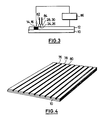
- FIG. 4 shows a thin-film solar cell assembly in a purely schematic and perspective representation in order to clarify that a plurality of parallel thin-film solar cells are arranged on the substrate (10) by the method steps described above, some of which are exemplified by the reference symbols ( 76), (78) and (80).
- the parallel thin-film solar cells (76), (78) and (80) are connected in series so that the thin-film solar cell array can deliver the desired voltage.
- a tool can preferably be used, which can be seen purely schematically in FIG. 3.
- the first electrode layer (12) arranged on the substrate (10) is preferably structured from TCO by means of spark erosion in order to form the strip-shaped regions (14) and (16).
- the tool has nozzles (82) and (84), via which the paste strips (24), (26) and (28), (30) run parallel to the areas (14) and (16) on the surface of the Electrode layer (12) are applied.
- the strip material (24), (26), as mentioned, is preferably stoving silver paste, whereas the material of the strips (28) and (30) is a paste with preferably TiO2.
- Spark erosion itself is indicated by the flash above areas (14), (16).
- the discharge takes place via a scalpel-shaped electrode.
- a current generator (86) In order for the spark discharge to occur, a current generator (86) must be provided, one pole of which is connected to the surface of the electrode layer (12) and the other pole of which is connected to the scalpel-shaped electrode, not shown.
- the tool shown in FIG. 3 can be modified in such a way that it is designed as a multiple tool, i.e. 4, a plurality of scalpel electrodes and nozzles (82) and (84) can be arranged next to one another in order to simultaneously specify the structure of a plurality of thin-film solar cells arranged parallel to one another.
Landscapes
- Photovoltaic Devices (AREA)
Applications Claiming Priority (2)
| Application Number | Priority Date | Filing Date | Title |
|---|---|---|---|
| DE19873712589 DE3712589A1 (de) | 1987-04-14 | 1987-04-14 | Verfahren zur herstellung von in reihe verschalteten duennschicht-solarzellen |
| DE3712589 | 1987-04-14 |
Publications (3)
| Publication Number | Publication Date |
|---|---|
| EP0286918A2 true EP0286918A2 (fr) | 1988-10-19 |
| EP0286918A3 EP0286918A3 (en) | 1989-11-02 |
| EP0286918B1 EP0286918B1 (fr) | 1992-06-03 |
Family
ID=6325579
Family Applications (1)
| Application Number | Title | Priority Date | Filing Date |
|---|---|---|---|
| EP88105204A Expired - Lifetime EP0286918B1 (fr) | 1987-04-14 | 1988-03-30 | Procédé pour la fabrication des piles solaires à couche mince connectées en serie |
Country Status (7)
| Country | Link |
|---|---|
| US (1) | US4929281A (fr) |
| EP (1) | EP0286918B1 (fr) |
| JP (1) | JPS6453583A (fr) |
| CN (1) | CN1037052A (fr) |
| AU (1) | AU1457188A (fr) |
| DE (2) | DE3712589A1 (fr) |
| IN (1) | IN171442B (fr) |
Cited By (2)
| Publication number | Priority date | Publication date | Assignee | Title |
|---|---|---|---|---|
| DE102007062620A1 (de) * | 2007-12-22 | 2009-07-09 | Schott Solar Gmbh | Verfahren und Vorrichtung zur Herstellung eines semitransparenten photovoltaischen Moduls |
| FR2972659A1 (fr) * | 2011-03-18 | 2012-09-21 | Commissariat Energie Atomique | Procede de traitement par electroerosion d'une surface d'un element en silicium et plaque de silicium obtenue grace a un tel traitement |
Families Citing this family (16)
| Publication number | Priority date | Publication date | Assignee | Title |
|---|---|---|---|---|
| CA2024662A1 (fr) * | 1989-09-08 | 1991-03-09 | Robert Oswald | Module photovoltaique monolithique a elements montes en serie et en parallele |
| US5289999A (en) * | 1990-07-04 | 1994-03-01 | Schottel Werft Joseph Becker Gmbh & Co. Kg | Apparatus for mounting solar cells |
| DE4306404A1 (de) * | 1993-03-02 | 1994-09-08 | Abb Research Ltd | Modul und Verfahren zu dessen Herstellung |
| DE19651655C2 (de) * | 1996-07-28 | 2002-10-02 | Rwe Solar Gmbh | Verschaltete Solarzellen, insbesondere seriell verschaltete Dünnschicht-Solarmodule, und Verfahren zu ihrer Herstellung |
| US6841728B2 (en) * | 2002-01-04 | 2005-01-11 | G.T. Equipment Technologies, Inc. | Solar cell stringing machine |
| JP4762100B2 (ja) * | 2006-09-28 | 2011-08-31 | 三洋電機株式会社 | 太陽電池モジュール |
| US8322025B2 (en) * | 2006-11-01 | 2012-12-04 | Solarworld Innovations Gmbh | Apparatus for forming a plurality of high-aspect ratio gridline structures |
| TW200849621A (en) * | 2006-12-21 | 2008-12-16 | Helianthos Bv | Method for making solar sub-cells from a solar cell |
| EP2073269A1 (fr) * | 2007-12-21 | 2009-06-24 | Helianthos B.V. | Procédé pour la fourniture d'une connexion en série dans un système de cellule solaire |
| JP4986945B2 (ja) * | 2008-07-25 | 2012-07-25 | 三洋電機株式会社 | 太陽電池の製造方法 |
| EP2416377B1 (fr) | 2009-03-31 | 2015-07-01 | LG Innotek Co., Ltd. | Cellule solaire et son procédé de production |
| WO2010118906A2 (fr) | 2009-04-16 | 2010-10-21 | Applied Materials, Inc. | Module photovoltaïque à film mince |
| EP2242109A1 (fr) | 2009-04-16 | 2010-10-20 | Applied Materials, Inc. | Module solaire à couche mince |
| JP2011023442A (ja) * | 2009-07-14 | 2011-02-03 | Seiko Epson Corp | 太陽電池、太陽電池の製造方法 |
| JP2013110341A (ja) * | 2011-11-24 | 2013-06-06 | Kyocera Corp | 光電変換装置 |
| CN104425637A (zh) | 2013-08-30 | 2015-03-18 | 中国建材国际工程集团有限公司 | 部分透明的薄层太阳能模块 |
Family Cites Families (14)
| Publication number | Priority date | Publication date | Assignee | Title |
|---|---|---|---|---|
| US3617376A (en) * | 1967-03-16 | 1971-11-02 | North American Rockwell | Antisublimation coating and method for thermoelectric materials |
| JPS50134391A (fr) * | 1974-04-09 | 1975-10-24 | ||
| US4178524A (en) * | 1976-09-01 | 1979-12-11 | Ritter James C | Radioisotope photoelectric generator |
| GB1575888A (en) * | 1977-09-08 | 1980-10-01 | Photon Power Inc | Solar cell array |
| US4525223A (en) * | 1978-09-19 | 1985-06-25 | Noboru Tsuya | Method of manufacturing a thin ribbon wafer of semiconductor material |
| DE2841465B2 (de) * | 1978-09-23 | 1980-08-21 | Messerschmitt-Boelkow-Blohm Gmbh, 8000 Muenchen | Vorrichtung zum Verschweißen von Kontaktfahnen mit Sonnenzellen |
| US4181755A (en) * | 1978-11-21 | 1980-01-01 | Rca Corporation | Thin film pattern generation by an inverse self-lifting technique |
| GB2108755B (en) * | 1981-09-26 | 1985-07-10 | Matsushita Electric Industrial Co Ltd | Thin film devices having diffused interconnections |
| US4724011A (en) * | 1983-05-16 | 1988-02-09 | Atlantic Richfield Company | Solar cell interconnection by discrete conductive regions |
| US4697041A (en) * | 1985-02-15 | 1987-09-29 | Teijin Limited | Integrated solar cells |
| EP0193820A3 (fr) * | 1985-02-27 | 1988-01-07 | Kanegafuchi Kagaku Kogyo Kabushiki Kaisha | Procédé pour former un dessin dans un film mince |
| JPS6233477A (ja) * | 1985-08-07 | 1987-02-13 | Sanyo Electric Co Ltd | 光起電力装置の製造方法 |
| DE3545385A1 (de) * | 1985-12-20 | 1987-06-25 | Messerschmitt Boelkow Blohm | Verfahren zur herstellung einer solarzellenanordnung |
| US4710588A (en) * | 1986-10-06 | 1987-12-01 | Hughes Aircraft Company | Combined photovoltaic-thermoelectric solar cell and solar cell array |
-
1987
- 1987-04-14 DE DE19873712589 patent/DE3712589A1/de active Granted
-
1988
- 1988-03-30 EP EP88105204A patent/EP0286918B1/fr not_active Expired - Lifetime
- 1988-03-30 DE DE8888105204T patent/DE3871598D1/de not_active Expired - Fee Related
- 1988-03-31 US US07/176,268 patent/US4929281A/en not_active Expired - Fee Related
- 1988-04-05 IN IN281/CAL/88A patent/IN171442B/en unknown
- 1988-04-13 AU AU14571/88A patent/AU1457188A/en not_active Abandoned
- 1988-04-14 CN CN88102268A patent/CN1037052A/zh active Pending
- 1988-04-14 JP JP63092640A patent/JPS6453583A/ja active Pending
Cited By (3)
| Publication number | Priority date | Publication date | Assignee | Title |
|---|---|---|---|---|
| DE102007062620A1 (de) * | 2007-12-22 | 2009-07-09 | Schott Solar Gmbh | Verfahren und Vorrichtung zur Herstellung eines semitransparenten photovoltaischen Moduls |
| FR2972659A1 (fr) * | 2011-03-18 | 2012-09-21 | Commissariat Energie Atomique | Procede de traitement par electroerosion d'une surface d'un element en silicium et plaque de silicium obtenue grace a un tel traitement |
| WO2012126834A1 (fr) * | 2011-03-18 | 2012-09-27 | Commissariat A L'energie Atomique Et Aux Energies Alternatives | Procede de fabrication d'une cellule photovoltaique comprenant une phase d'electroerosion |
Also Published As
| Publication number | Publication date |
|---|---|
| EP0286918A3 (en) | 1989-11-02 |
| DE3712589C2 (fr) | 1991-09-19 |
| CN1037052A (zh) | 1989-11-08 |
| DE3871598D1 (de) | 1992-07-09 |
| US4929281A (en) | 1990-05-29 |
| IN171442B (fr) | 1992-10-17 |
| DE3712589A1 (de) | 1988-11-03 |
| AU1457188A (en) | 1988-10-20 |
| JPS6453583A (en) | 1989-03-01 |
| EP0286918B1 (fr) | 1992-06-03 |
Similar Documents
| Publication | Publication Date | Title |
|---|---|---|
| DE3121350C2 (de) | Verfahren zum Herstellen einer Sonnenbatterie | |
| DE3712589C2 (fr) | ||
| DE3604917C2 (fr) | ||
| DE3686195T2 (de) | Zusammenschaltung von solarzellen mittels unterbrochener leitender bereiche. | |
| EP2168177B1 (fr) | Méthode de fabrication d'un module de piles solaires en couches minces | |
| DE4344693B4 (de) | Dünnfilmsolarzellenanordnung | |
| DE3210742A1 (de) | Solarzellenbatterie und verfahren zum herstellen der batterie | |
| DE2919114A1 (de) | Photovoltaische zellen in feldanordnung und verfahren zur herstellung derselben | |
| EP2507834B1 (fr) | Procédé pour enlever au moins dans certaines zones une couche d'un empilement de couches | |
| WO2011032717A2 (fr) | Interconnexion série de photopiles en minces couches | |
| DE102009021273A1 (de) | Verfahren und Vorrichtung zur Herstellung eines photovoltaischen Dünnschichtmoduls | |
| DE2839038C2 (fr) | ||
| EP2058870A2 (fr) | Mise en contact et connexion de module de cellules solaires à couche fine sur des supports polymères | |
| DE3704437C2 (fr) | ||
| DE112005002629T5 (de) | Ultraleichte Photovoltaik-Einrichtung und Verfahren zu deren Herstellung | |
| DE102016106563A1 (de) | Verfahren zum Herstellen einer Solarzelle, mit dem Verfahren hergestellte Solarzelle und Substratträger | |
| DE3714920C1 (de) | Verfahren zur Herstellung einer Duennschicht-Solarzellenanordnung | |
| DE3545385C2 (fr) | ||
| EP2151870A2 (fr) | Procédé destiné à la fabrication d'un module photovoltaïque | |
| DE102008029107B4 (de) | Verfahren zur Herstellung einer Metallstruktur auf einer Oberfläche eines Halbleitersubstrates | |
| DE102020126436B4 (de) | Verfahren zur Herstellung eines Metall-Halid Perowskit SolarmodulsAnspruch 4: offensichtlicher Fehler korrigiert (Ansprüche 2 oder 3 anstelle von Ansprüche 3 oder 4) | |
| DE102009035703B4 (de) | Verfahren zur Herstellung von Verbünden flexibler Dünnschichtsolarzellen | |
| DE19814780A1 (de) | Fotovoltaisches Bauelement | |
| WO2012072062A2 (fr) | Procédé de fabrication d'un module solaire et module solaire | |
| DE102023107348A1 (de) | Verfahren zum fertigen einer dünnschichtsolarzelle, insbesondere perowskitsolarzelle, sowie dünnschichtsolarzelle und tandemsolarzelle |
Legal Events
| Date | Code | Title | Description |
|---|---|---|---|
| PUAI | Public reference made under article 153(3) epc to a published international application that has entered the european phase |
Free format text: ORIGINAL CODE: 0009012 |
|
| AK | Designated contracting states |
Kind code of ref document: A2 Designated state(s): CH DE ES FR GB IT LI |
|
| PUAL | Search report despatched |
Free format text: ORIGINAL CODE: 0009013 |
|
| AK | Designated contracting states |
Kind code of ref document: A3 Designated state(s): CH DE ES FR GB IT LI |
|
| 17P | Request for examination filed |
Effective date: 19891116 |
|
| 17Q | First examination report despatched |
Effective date: 19910118 |
|
| GRAA | (expected) grant |
Free format text: ORIGINAL CODE: 0009210 |
|
| AK | Designated contracting states |
Kind code of ref document: B1 Designated state(s): CH DE ES FR GB IT LI |
|
| PG25 | Lapsed in a contracting state [announced via postgrant information from national office to epo] |
Ref country code: IT Free format text: LAPSE BECAUSE OF FAILURE TO SUBMIT A TRANSLATION OF THE DESCRIPTION OR TO PAY THE FEE WITHIN THE PRE;WARNING: LAPSES OF ITALIAN PATENTS WITH EFFECTIVE DATE BEFORE 2007 MAY HAVE OCCURRED AT ANY TIME BEFORE 2007. THE CORRECT EFFECTIVE DATE MAY BE DIFFERENT FROM THE ONE RECORDED.SCRIBED TIME-LIMIT Effective date: 19920603 Ref country code: GB Effective date: 19920603 Ref country code: ES Free format text: THE PATENT HAS BEEN ANNULLED BY A DECISION OF A NATIONAL AUTHORITY Effective date: 19920603 |
|
| REF | Corresponds to: |
Ref document number: 3871598 Country of ref document: DE Date of ref document: 19920709 |
|
| ET | Fr: translation filed | ||
| GBV | Gb: ep patent (uk) treated as always having been void in accordance with gb section 77(7)/1977 [no translation filed] | ||
| PG25 | Lapsed in a contracting state [announced via postgrant information from national office to epo] |
Ref country code: LI Effective date: 19930331 Ref country code: CH Effective date: 19930331 |
|
| PLBE | No opposition filed within time limit |
Free format text: ORIGINAL CODE: 0009261 |
|
| STAA | Information on the status of an ep patent application or granted ep patent |
Free format text: STATUS: NO OPPOSITION FILED WITHIN TIME LIMIT |
|
| 26N | No opposition filed | ||
| REG | Reference to a national code |
Ref country code: CH Ref legal event code: PL |
|
| PGFP | Annual fee paid to national office [announced via postgrant information from national office to epo] |
Ref country code: DE Payment date: 19960328 Year of fee payment: 9 |
|
| PGFP | Annual fee paid to national office [announced via postgrant information from national office to epo] |
Ref country code: FR Payment date: 19960329 Year of fee payment: 9 |
|
| PG25 | Lapsed in a contracting state [announced via postgrant information from national office to epo] |
Ref country code: FR Free format text: LAPSE BECAUSE OF NON-PAYMENT OF DUE FEES Effective date: 19971128 |
|
| PG25 | Lapsed in a contracting state [announced via postgrant information from national office to epo] |
Ref country code: DE Effective date: 19971202 |
|
| REG | Reference to a national code |
Ref country code: FR Ref legal event code: ST |